Table of Contents
Advertisement
Quick Links
Advertisement
Table of Contents

Subscribe to Our Youtube Channel
Related Manuals for Flex ROA128 6016


Summary of Contents for Flex ROA128 6016
- Page 1 Evaluation Board User Guide BMR474 ROA 128 6016 USER GUIDE...
- Page 2 The contents of this document are subject to revision without notice due to continued progress in methodology, design and manufacturing. Flex shall have no liability for any error or damage of any kind resulting from the use of this document.
-
Page 3: Table Of Contents
How to contact Flex.................. 4 Prerequisites .................... 4 Reference Board ROA 128 6016 ............5 USB-PMBus adapter ................7 Connection of Flex KEP 910 17 USB-PMBus adapter ......7 Power-up and Power-down Instructions ..........7 Power-up instruction ................7 Power-down instruction ................8 Address and VSET Resistor .............. -
Page 4: Introduction
In order to operate the ROA 128 6016 board, the following is needed: Power supply 6 – 15 V. USB-PMBus adapter Flex KEP 910 17. It is only needed when the PMBus shall be used. The “Flex Power Designer” software package and a compatible Windows... -
Page 5: Reference Board Roa 128 6016
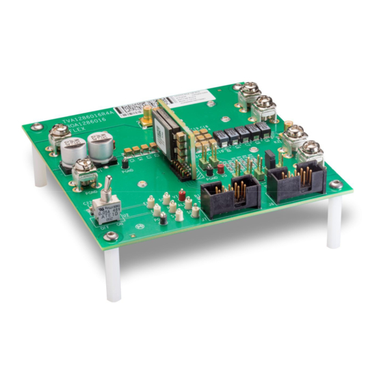
Test Board User Guide BMR474 Reference Board ROA 128 6016 In Figure 1a and 1b, the top and bottom sides of the ROA 128 6016 are shown. Figure 1a. ROA 128 6016 (top side) 28701-ROA1286016 Rev A 2021/4/25 5 (20) - Page 6 Test Board User Guide BMR474 Figure 1b. ROA 128 6016 (bottom side) Position Description (Top Side) Input voltage connectors. Output voltage connectors. Power Good LED. ENABLE switch. Connector for the USB-PMBus adaptor (KEP 910 17). SMB Oscilloscope connectors for Vin ripple measurement SMB Oscilloscope connectors for Vo ripple measurement Input electrolytic and ceramic capacitors.
-
Page 7: Usb-Pmbus Adapter
Positions for additional output ceramic capacitors USB-PMBus adapter The USB-PMBus adapter used with this board is the Flex KEP 910 17. Connection of Flex KEP 910 17 USB-PMBus adapter Connect the Flex KEP 910 17 USB-PMBus adapter to the PMBus header, see position 5 in Figure 1a. -
Page 8: Power-Down Instruction
Test Board User Guide BMR47401 Model Iout max Switching frequency Vin/Vout range 0.6V≤ Vo ≤1.8V 0.6V≤ Vo ≤1.8V Vin =6-15 V =500kHz Iomax=80A 0.6V≤ Vo ≤2.5V BMR 474 2001 1.8V < Vo ≤3.3V 1.8V < Vo ≤3.3V Vin=7.5-15V =800kHz Iomax=60A 2.5V <... -
Page 9: Address And Vset Resistor
Test Board User Guide BMR47401 Address and VSET Resistor Adjustment of address resistor To change the address, change the resistor shown in Figure 2. Change R4 and R5 (position 11) to achieve the desired PMBus address for the module. ... -
Page 10: Additional Input/Output Capacitance
Test Board User Guide BMR47401 Additional Input/output Capacitance At the bottom side, there are places for additional input/output capacitors. additional input additional output capacitors capacitors Figure 3 Places for additional input/output capacitors. Electronic loads In order to perform load transient tests on the modules, up to 2 pcs of PuLS loads can be connected to the output of the board. -
Page 11: Schematic
Test Board User Guide BMR47401 The PuLS loads (ROA 128 5552) can be programmed for different transient loads and waveforms, see the technical specification for further information. The PuLS loads can be easily connected through the sockets. (see position 17 in Fig 1b) Schematic See schematic of Board ROA 128 6016 for more information. -
Page 12: Layout Description
Test Board User Guide BMR47401 C10,C11,C12,C13,C14,C15, 100uF 10% 1210 6.3V X7S,CAPACITOR C16,C17,C18,C19,C20,C21 100nF 10% 0805 25V X7R,CAPACITOR C22,C50 100nF 10% 0603 25V X7R,CAPACITOR C24,C26 LED, green PMBus connector J7,J8 Ferrite Bead L1,L2,L3,L4,L5,L6 0ohm 0603 ,RESISTOR, -55C~155C R5, R16 68.1kohm 1% 0603 0.1W,RESISTOR, -55C~155C 6.65kohm 1% 0603 0.1W,RESISTOR, -55C~155C 115kohm 1% 0603 0.1W,RESISTOR, -55C~155C 6.34kohm 1% 0603 0.1W,RESISTOR, -55C~155C... - Page 13 Test Board User Guide BMR47401 Layer 2 VOUT, PGND plane, signal traces 2 oz Layer 3 VIN, VOUT, PGND planes 2 oz VIN, VOUT, PGND planes Bottom layer 2 oz Component footprints, signal traces Figure 4 Connection of power pins on top layer 28701-ROA1286016 Rev A 2021/4/25 13 (20)
-
Page 14: Input Capacitance
Test Board User Guide BMR47401 11.2 Input capacitance The ceramic input capacitors should be placed as close as possible to the VIN/PGND pins to minimize the connection impedance. For the same reason, multiple vias are placed close to the capacitors’ terminals, utilizing inner layers to connect to input pins of the module. -
Page 15: Layout Top View
Test Board User Guide BMR47401 Layout top view Top side component layout 28701-ROA1286016 Rev A 2021/4/25 15 (20) - Page 16 Test Board User Guide BMR47401 Top layer 28701-ROA1286016 Rev A 2021/4/25 16 (20)
- Page 17 Test Board User Guide BMR47401 Layer 2 28701-ROA1286016 Rev A 2021/4/25 17 (20)
- Page 18 Test Board User Guide BMR47401 Layer 3 28701-ROA1286016 Rev A 2021/4/25 18 (20)
- Page 19 Test Board User Guide BMR47401 Bottom Layer 28701-ROA1286016 Rev A 2021/4/25 19 (20)
- Page 20 Test Board User Guide BMR47401 Bottom side component layout 28701-ROA1286016 Rev A 2021/4/25 20 (20)
Need help?
Do you have a question about the ROA128 6016 and is the answer not in the manual?
Questions and answers