
Related Manuals for Embedded Artists LPC4357


Summary of Contents for Embedded Artists LPC4357
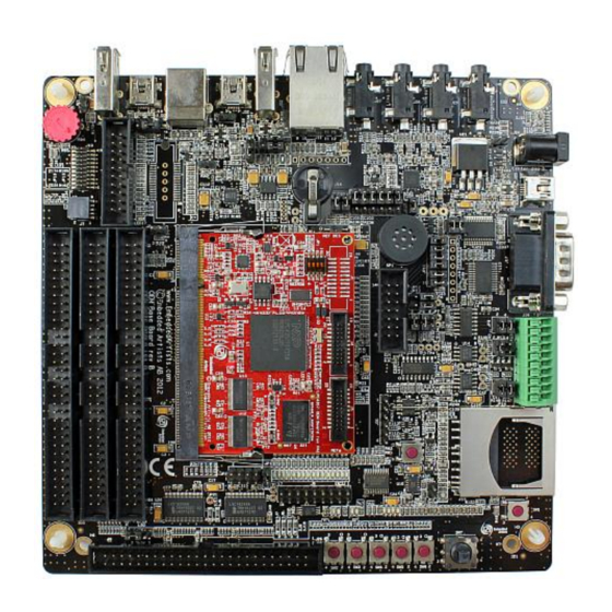
- Page 1 - User’s Guide LPC4357 Developer’s Kit Copyright 2018 © Embedded Artists AB LPC4357 Developer’s Kit User’s Guide Get Up-and-Running Quickly and Start Developing Your Application On Day 1! EA2-USG-1208 Rev A...
- Page 2 Embedded Artists AB. Disclaimer Embedded Artists AB makes no representation or warranties with respect to the contents hereof and specifically disclaim any implied warranties or merchantability or fitness for any particular purpose. Information in this publication is subject to change without notice and does not represent a commitment on the part of Embedded Artists AB.
-
Page 3: Table Of Contents
LPC4357 Developer’s Kit - User’s Guide Page 3 Table of Contents 1 Document Revision History 2 Introduction Features ESD Precaution 2.2.1 ESD sensitivity on JTAG interface General Handling Care Code Read Protection CE Assessment Other Products from Embedded Artists 2.6.1 Design and Production Services 2.6.2... - Page 4 USB Channel 1 as USB OTG 4.21 SP12: USB Channel 2 4.21.1 USB Channel 2 (USB0 on LPC4357) as USB Host 4.21.2 USB Channel 2 (USB0 on LPC4357) as USB Device 4.21.3 USB Channel 2 (USB0 on LPC4357) as USB OTG 4.22...
-
Page 5: Document Revision History
LPC4357 Developer’s Kit - User’s Guide Page 5 1 Document Revision History Revision Date Description 2012-10-29 First version. 2012-12-08 Added information about ESD sensitive JTAG interface. 2013-01-21 Minor clarifications. 2013-04-08 Clarified that JP4 must be shorted (jumper installed) in order for the LPC4357 SWD/JTAG interface to function. -
Page 6: Introduction
Thank you for buying Embedded Artists’ LPC4357 Developer’s Kit based on NXP’s ARM dual-core Cortex-M4/M0 LPC4357 microcontroller. This document is a User’s Guide that describes the LPC4357 OEM Board and the OEM Base Board hardware design, which together form the LPC4357 Developer’s Kit. -
Page 7: Esd Precaution
ESD. Never touch directly on the LPC4357 OEM Board and in general as little as possible on the OEM Base Board. The push-buttons on the OEM Base Board have grounded shields to minimize the effect of ESD. -
Page 8: Esd Sensitivity On Jtag Interface
LPC4357 Developers Kit. Due to the nature of the LPC4357 Developers Kit – an evaluation board not for integration into an end- product – fast transient immunity tests and conducted radio-frequency immunity tests have not been executed. -
Page 9: Other Products From Embedded Artists
Page 9 Other Products from Embedded Artists Embedded Artists have a broad range of LPC1000/2000/3000/4000 based boards that are very low cost and developed for prototyping / development as well as for OEM applications. Modifications for OEM applications can be done easily, even for modest production volumes. Contact Embedded Artists for further information about design and production services. -
Page 10: Lpc4357 Oem Board Design
As seen in the table above, it is only the static memory regions that are available on the external memory bus from the LPC4357 OEM Board. The data bus buffers on the LPC4357 OEM Board are controlled automatically and only enabled when a static memory region is accessed. The address and control bus buffers are always enabled. -
Page 11: Spifi
GPIO72 by inserting a jumper between pin 3-4 on JP2. The busy status of the chip is also available under software control. SPIFI There is a 16 MBit QSPI flash connected to the SPIFI interface of the LPC4357. This memory region is available in the following address region: 0x1400 0000 – 0x1800 0000. Bootloader Mode Setting There are several boot modes for the LPC4357 microcontroller. -
Page 12: Trace Connector
I2S and SGPIO Connectors There are two 20-pos, 50 mil pitch connectors on the top side of the LPC4357 OEM board. See Figure 1 for location. These connectors carry selected I2S, I2C, SGPIO and SCT signals and can be used to connect these signals to a separate expansion boards. -
Page 13: Board Options
Page 13 Board Options The schematic for the LPC4357 OEM Board show some different mounting options, mainly via SJx jumpers but also some resistors that are not mounted per default. The design has been prepared for customized versions for different needs. -
Page 14: Oem Base Board Design
LPC4357 Developer’s Kit - User’s Guide Page 14 4 OEM Base Board Design This chapter contains information about the peripherals and general design of the OEM Base Board and how to set the different jumpers on the board. The schematic can be downloaded in pdf format from the support page, and is recommended to have printed out while reading this chapter. -
Page 15: Sp2: Oem Board Connector
LPC4357 signal names. This is because the OEM base board also supports other OEM boards. SP2: Current Measurements It is possible to accurately measure current consumption of the LPC4357 OEM board. This can be very valuable when working with applications that make use of the low power modes of the LPC4357 processors. -
Page 16: Sp4: External Memory Bus
Signals BBLS0/BBLS1 controls the lower and upper 8 bits, respectively. Since the OEM Base Board is universal and supports many different OEM Boards, the chip select signal is either signal BCSX or GPIO69. For the LPC4357 OEM Board, the signal BCSX is actually Copyright 2018 © Embedded Artists AB... -
Page 17: Sp5: Debug Interfaces
Figure 6 – External Memory Bus Circuit SP5: Debug Interfaces Note that the LPC4357 MCU is sensitive to ESD on the JTAG port. Observe extra care around this. Make sure the ground of the JTAG interface is connected to the OEM Base Board ground before even connecting the JTAG interface. - Page 18 When working with the LPC4357 OEM Board, J7 is typically used. If an older and big footprint JTAG debug pod is used, J8 can alternatively be used. If trace is also used, use the connector J1 on the LPC4357 OEM board. Note that this requires an advanced JTAG probe that supports trace.
-
Page 19: Sp6: Ethernet Interface
LPC4357 Developer’s Kit - User’s Guide Page 19 SP6: Ethernet Interface The board has an Ethernet interface, J11, which is a RJ45 connector with integrated magnetics. There is also provision on the board for connecting a PoE interface. All signals can be accessed via expansion pads, J12. -
Page 20: Sp6: Sd/Mmc Memory Card Interface
MCI peripheral interface of the LPC4350. Instead, there is a uSD/transflash memory card interface on the bottom side of the LPC4357 OEM board. There is visual indication via LED2 on the LPC4357 OEM board that supply voltage to the memory card is present. -
Page 21: Sp6: Vbat/Alarm Handling
A 3V Lithium CR1025 size coin battery, via D2. Note that battery is not included. See the LPC4357 datasheet for details about VBAT voltage range. The ALARM signal control LED21. Note that LED21 will consume a lot of current from the battery and/or super-capacitor. -
Page 22: Sp7: I2C Peripherals
LPC4357 Developer’s Kit - User’s Guide Page 22 4.10 SP7: I2C Peripherals There are several I2C peripherals on the board. See picture below for locating the different components on the board. The I2C addresses for the individual components are given in the schematic. -
Page 23: Sp8: Analog Input
It is recommended to remove resistor R93 on the OEM base board in order to be able to use signal ADC6. In order to be compatible with other OEM boards, R93 connects signal V3A and VREF, but signal VREF is carrying signal ADC6 on the LPC4357 OEM board. Trimming Potentiometer Figure 12 –... -
Page 24: Sp8: Digital Io
There is a push-button (SW6) that is connected to a signal that enable the ISP-mode after reset on the OEM Board. For the LPC4357 this is pin P2_7. If this pin is sampled low after reset, the ISP-mode for the LPC4357 is entered. LED30 is positioned above SW6 and will light when SW6 is pressed. It is also possible to control LED30 as an output from the OEM Board without damaging the output driver when SW6 is pressed. - Page 25 Also note that pin 13 and 14 on the Serial Expansion Connector, J15, are connected to ADC1 and ADC2, respectively. These pins are input only on the LPC4357. In order to have GPIO functionality on these two pins on J15, other GPIO signals has to be wired to these pins. This can easily be done at the J3, J5 and J5 connectors.
-
Page 26: Sp8: Nxp/Jennic Rf Module Interface
SW9 during (and shortly after) reset. Note that the UART channel is not directly connected to a UART channel on the LPC4357. It is multiplexed with other UART channels, see section 4.15 for details. Also note that the Serial Expansion Connector (see section 4.13 ) and the RF-module share the same UART channel. -
Page 27: Sp9: Uart Multiplexing
LPC4357 Developer’s Kit - User’s Guide Page 27 4.15 SP9: UART Multiplexing UART channels from four sources are multiplexed into one UART channel, which is connected to the OEM Board: Serial Expansion Connector / RF module. Note that if the RF module is soldered to the board, then UART channel on the Serial Expansion Connector is occupied. -
Page 28: Sp9: Rs232 Interface
See picture below for locating relevant components on the board. The table below lists signal connections. Note that for the LPC4357 OEM board, which has 32-bit databus, the UART signals (Rx/Tx and modem signals) are not available at the same place as other OEM boards. The upper half of the databus occupies the signals used in this interface. -
Page 29: Sp9: Rs422/485 Interface
LPC4357 Developer’s Kit - User’s Guide Page 29 4.17 SP9: RS422/485 Interface There is a RS422/485 interface on the board. RS422 has individual transmit and receive pairs, while RS485 share the same signal pair (and is hence half-duplex). By inserting both jumpers in JP9, the two signal pairs are connected and a RS485 interface is created. -
Page 30: Sp10: Can
There is one CAN interface mounted on the board. The board is also prepared for a second CAN interface, but this cannot be used with the LPC4357 OEM board. Via JP16 it is also possible to add termination resistors, if needed. The interface has on-board ESD protection. -
Page 31: Sp10: Irda
4.19 SP10: IrDA The board is prepared for an IrDA interface, but the IrDA transceiver (TFBS4652) is not mounted. Note that the pinning of the LPC4357 OEM board is not compatible with the IrDA interface, which cannot be used. IrDA Transceiver Figure 20 –... -
Page 32: Sp11: Usb Channel
GPIO46 is by default disconnected as well as status feedback from the distribution switch via GPIO51. In case VBUS1 shall be actively controlled from the LPC4357 OEM Board, R190 and R198 must be soldered and pad 2-3 on SJ5 must be connected. Further, GPIO43/46/51 must not be used for other tasks in the design. -
Page 33: Usb Channel 1 As Usb Host
LPC4357 Developer’s Kit - User’s Guide Page 33 GPIO42 P9_6 GPIO51 PB_2 (dual functions) GPIO52 PB_1 GPIO53 PB_0 GPIO46 P8_3 normally not connected GPIO43 PF_6 normally not connected 4.20.1 USB Channel 1 as USB Host When USB channel #1 is used as USB Host, 15Kohm pull-down resistors are needed on the USB data signals. -
Page 34: Sp12: Usb Channel
The software on the LPC4357 OEM Board is also different between the two interfaces. This interface is connected to the USB0 interface on the LPC4357. For USB Device operation; insert jumpers in position 1-2 in JP17/JP18/JP19. GPIO28 controls USB connect functionality and LED32 lights when the USB Device is connected. -
Page 35: Usb Channel 2 (Usb0 On Lpc4357) As Usb Host
4.21.3 USB Channel 2 (USB0 on LPC4357) as USB OTG The USB0 interface of the LPC4357 supports USB OTG directly. JP17/JP18/JP19 shall all be set in position 2-3. J32 is the connector to use when USB OTG is used. This is a mini-AB USB connector. The VBUS signal is also feed back to GPIO54. -
Page 36: Sp13: Uart-To-Usb Bridge
PC side. The driver creates a virtual COM port on the PC that represents the UART channel. Any program on the PC can connect to this COM port for communication with the LPC4357 UART channel. There are two LEDs (Transmit – LED38 and Receive – LED37) that signal communication activity. -
Page 37: Sp13: Power Supply
LPC4357 Developer’s Kit - User’s Guide Page 37 4.23 SP13: Power Supply The power supply on the board is straight forward. There are three powering sources: 1. +5V DC via 2.1mm power jack (J24). Center pin positive. There is also an alternative connector (J23) for this powering option. -
Page 38: Sp15: I2S Audio Codec
LPC4357 Developer’s Kit - User’s Guide Page 38 On rev B of the OEM base board, JP34 has been added to support the LPC4357 OEM board. JP34 shall be in position 2-3 to route signal LCD_VD3 properly (to where LCD_VD18 otherwise is). The reason for this is for backward compatibility with previous OEM board designs. - Page 39 The board also has an on-board speaker. The right line output can be used to drive the speaker. The analog output from the LPC4357 as well (signal GPIO40). See picture below for locating relevant components. The table below lists signal connections.
-
Page 40: Default Jumpers Positions
Figure 27 – OEM Base Board Default Jumper Positions Note that the default position for the six I2S jumpers is not what is needed for the LPC4357 OEM board. Also, JP34 is in wrong position. Before working with I2S audio and the LCD interface change the jumper settings. -
Page 41: Usage Of Cpu Pins
Page 41 4.27 Usage of CPU Pins Almost all pins of the LPC4357 are directly available on the expansion connectors. Only in a few cases are pins used for dedicated functionality like Ethernet interface and chip select signals. Such pins are not available on the expansion connector. - Page 42 LPC4357 Developer’s Kit - User’s Guide Page 42 CAN interface not supported by LPC4357 OEM board pinning. GPIO19 P4_4 LCD databit 1, can also be connected to TD2 for CAN channel CAN interface not supported by LPC4357 OEM board pinning.
- Page 43 USB0-DP/DM Connects to USB Host/Device interface MCICLK PF_5 Connects to MCICLK on SD/MMC connector Note that LPC4357 OEM Board pinning does not support the MCI interface. Use uSD/transflash memory card interface on LPC4357 OEM board instead. MCICMD PC_11 Connects to MCICMD on SD/MMC connector Note that LPC4357 OEM Board pinning does not support the MCI interface.
- Page 44 Can be connected to I2S audio codec SYSCLK. GPIO69 P9_2 Can be used as chip select for 16-bit register on external memory bus, but not for the LPC4357. Can be used as enable signal for IrDA transceiver (active low). GPIO70 P8_1 Connects to LCD expansion connector (interrupt signal from touch screen controller).
- Page 45 Connected to SWD/JTAG connectors signals signals Note that the LPC4357 MCU is sensitive to ESD on the JTAG port. Observe extra care around this. Make sure the ground of the JTAG interface is connected to Copyright 2018 © Embedded Artists AB...
- Page 46 LPC4357 Developer’s Kit - User’s Guide Page 46 the OEM Base Board ground before even connecting the JTAG interface. Never have the OEM Board unpowered while the JTAG pod is powered. RESET_IN RESET Connects to RESET push-button and USB-to-serial bridge (for...
-
Page 47: Getting Started
The LPC4357 Developer’s Kit comes pre-loaded with a demo application. If the demo application is missing or over-written by another application, follow the guidelines for how to download a program to the LPC4357, see section 5.4 . The source code and pre-compiled hex-file is available on the support site. - Page 48 Version: 1.0, (build October 24 2012) LCD controller; the program will detect if a display (one of Embedded Artists’ LCD boards) is connected on the LCD Expansion Connector and display an image on it, like below. Figure 29 – Demo Application Image...
-
Page 49: Installing Usb Driver
The OEM Base Board contains an USB-to-UART bridge chip (FT232R from FTDI) that connects UART channel #0 on the LPC4357 to a virtual COM port on the PC/laptop (via USB). This UART channel is typically used as the console channel for applications. Printf() output can for example be directed to this UART channel. -
Page 50: Isp Over Usb Program Download
TP6/TP7 are found in the upper left corner of the pcb. IAP over Ethernet or USB IAP is short for In-Application Programming. In this case, the LPC4357 must have a small bootloader installed that allow application code to be downloaded over Ethernet, USB or some other communication channel. - Page 51 LPC4357 Developer’s Kit - User’s Guide Page 51 A *.bin file must be created. In Keil uVision this is done by adding the following user command: fromelf --bin -o "$L@L.bin" "$L@L.axf" See the project files in the sample applications for how it is added to the compile process.
- Page 52 LPC4357 Developer’s Kit - User’s Guide Page 52 4. For “File”, select the *.bin file that has been generated to be downloaded 5. For “Address”, enter 0x1A000000 6. For “Size”, enter 0x00080000 7. The “Param” field is not used so leave it as default 8.
-
Page 53: Handling So-Dimm Boards
OEM Board edge connectors. Handle the OEM Board only by the three other edges. Also, do not touch the components on the board. Things to Note This section lists things to note when using the LPC4357 OEM Board and the OEM Base Board. 5.6.1 Low Speaker Audio Volume The speaker audio volume can be low on some OEM Base Board, rev C boards produced in Q1-2018. -
Page 54: Humming In Speaker
LPC4357 Developer’s Kit - User’s Guide Page 54 R238 – add 6.8Kohm resistor in parallel R236 – add 6.8Kohm resistor in parallel Figure 34 – R236/R238 Location on OEM Base Board, rev C 5.6.2 Humming in Speaker In some situations there can be a humming sound from the on-board speaker. This is because of high- frequency noise on signal GPIO40_AOUT. -
Page 55: Current Consumption And Limits Of Usb Ports
Current Consumption and Limits of USB Ports The current consumption of LPC4357 OEM Board, OEM Base Board, and the 4.3 inch LCD Board is in the region of 450-525mA. This is very close to what a normal USB-A port can supply. If the boards are powered from a USB-A port (for example a PC or laptop) and there are problems, like spontaneous resets or other strange things, it is likely that an external power supply is needed. -
Page 56: Initialization Of External Memory Bus
Initialization of External Memory Bus The databus buffers (U12, U14 on LPC4357 OEM board) to the external memory bus are controlled by the OE and BLSx signals. Even though the external memory bus is not used, OE and BLSx are reserved and cannot be used for other purposes. -
Page 57: Lcd Expansion Connector
The LCD expansion connector carries 18 data bits per pixel by default (6 per RGB color). The LPC4357 LCD controller can produce 24 data bits per pixel and it is possible to output all these signals on the LCD expansion connector. The trade-off is that the UART and I2C serial interfaces have to be removed. - Page 58 In most cases the LPC4357 can generate the appropriate DOTCLK frequency. The higher the frequency needed, the fewer available frequencies can be selected when dividing the core clock. If a specific frequency is needed, the GP_CLKIN (pin PF_4) signal can be used. It is an input to the LPC4357.
- Page 59 As a final step a touch screen interface is typically needed. o Embedded Artists display boards often use the TSC2046 from TI. It has a simple SPI interface. o Capacitive touch screen controllers typically have I2C or SPI interfaces.
-
Page 60: Troubleshooting
It is strongly advised to read through the list of tests and actions that can be done before contacting Embedded Artists. The different tests can help determine if there is a problem with the board, or not. For return policy, please read Embedded Artists’ General Terms and Conditions http://www.embeddedartists.com/shop/... -
Page 61: Contact With Oem Board Mcu
PC. Contact with OEM Board MCU The second step is to make sure that the LPC4357 MCU on the OEM Board is working. Test that it is possible to download one of the precompiled test programs that exist on Embedded Artists support site. -
Page 62: Further Information
LPC4357 Developer’s Kit - User’s Guide Page 62 8 Further Information The LPC4357 microcontroller is a complex circuit and there exist a number of other documents with a lot more information. The following documents are recommended as a complement to this document. NXP LPC4357 Datasheet https://www.nxp.com/docs/en/data-sheet/LPC435X_3X_2X_1X.pdf...
Need help?
Do you have a question about the LPC4357 and is the answer not in the manual?
Questions and answers