Table of Contents
Advertisement
Quick Links
Advertisement
Table of Contents

Related Manuals for Texas Instruments DAC7554


Summary of Contents for Texas Instruments DAC7554
- Page 1 DAC7554 Evaluation Module User's Guide Literature Number: SLAU154 March 2005...
- Page 2 SLAU154 – March 2005...
-
Page 3: Table Of Contents
...................... EVM Stacking ................The Output Operational Amplifier ..................... Jumper Setting ......................Schematics ............Related Documentation From Texas Instruments ............. Questions About This or Other Data Converter EVMs? ......................Trademarks ....................... Important Notices SLAU154 – March 2005 Table of Contents... - Page 4 List of Figures ......................EVM Block Diagram ....................... Top Silkscreen ................Top Layer (Signal and Split Ground Plane) ................Bottom Layer (Signal and Split Ground Plane) ......................Bottom Silkscreen ........................ Drill Drawing ..................Factory Default Jumper Setting List of Tables ........................
-
Page 5: Evm Overview
Supply Voltage The dc power supply requirement for this DAC7554 EVM (VDD) is selectable between 3.3 V and 5 V via W1 jumper header. The 3.3 V comes from J6-8 or J5-1 (if installed), and the 5 V comes from J6-3 or J5-3 terminals (if installed), when plugged in via 5-6k interface card or the HPA449. -
Page 6: Evm Basic Functions
The headers J2 and P2 are the connectors provided to allow the control signals and data required to interface a host processor or waveform generator to the DAC7554 EVM using a custom built cable. An adapter interface card (5-6k adapter interface) is also available to fit and mate with TI’s TMS320C5000™... -
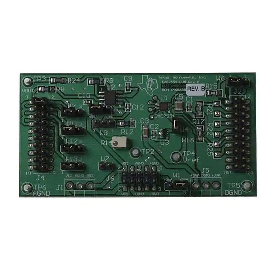
Page 7: Pcb Design And Performance
EVM. The list of components used on the module is also included in this section. PCB Layout The DAC7554 EVM is designed to preserve the performance quality of the DAC, device under test, as specified in the data sheet. Carefully analyzing the EVM’s physical restrictions and the given or known elements that contributes to the EVM’s performance degradation is the key to a successful design... -
Page 8: Top Silkscreen
PCB Design and Performance The DAC7554 EVM board is constructed on a two-layer printed-circuit board using a copper-clad FR-4 laminate material. The printed-circuit board has a dimension of 43,1800 mm (1.7000 inch) × 81,2800 mm (3.200 inch), and the board thickness is 1,5748 mm (0.0620 inch). Figures 2 through 6 show the individual artwork layers. - Page 9 www.ti.com PCB Design and Performance Figure 4. Bottom Layer (Signal and Split Ground Plane) Figure 5. Bottom Silkscreen SLAU154 – March 2005 DAC7554EVM...
-
Page 10: Drill Drawing
www.ti.com PCB Design and Performance Figure 6. Drill Drawing DAC7554EVM SLAU154 – March 2005... -
Page 11: Bill Of Materials
SSW-105-22-F-DVS-K TP2, TP3, TP4, TP_TURRENT Mill-Max 2348-2-01-00-00-07-0 TP5, TP6 8-SOP(D) High Precision OP-Amp MSOP-10(DGS) Texas Instruments OPA277UA DAC7554, 12-Bit, 4-CH, SPI Texas Instruments DAC7554 4.096V VOLTAGE REFERENCE SOT23-3 Texas Instruments REF3140AIDBZT W4, W7 2 CIRCUIT HEADER, 0.100 STRAIGHT Molex 22-03-2021 W1, W2, W3, 3 CIRCUIT HEADER, 0.100 STRAIGHT... -
Page 12: Evm Operation
This section covers in detail the operation of the EVM to provide guidance to the user in evaluating the onboard DAC and how to interface the EVM to a specific host processor. Refer to the DAC7554 data sheet, SLAS399A, for information about its serial interface and other related topics. -
Page 13: Host Processor Interface
EVM Stacking The stacking of EVM is possible if there is a need to evaluate two DAC7554 to yield a total of eight channel output. A maximum of two EVMs are allowed since the output terminal, J4, dictates the number of DAC channels that can be connected without colliding. -
Page 14: Unity Gain Output Jumper Settings
This is the default configuration that the EVM is set to from the factory. The buffered output configuration can be used to prevent loading the DAC7554 though it may present some slight distortion because of the feedback resistor and capacitor. The user can tailor the feedback circuit to closely match their desired wave shape by simply desoldering R7 and C11 and replacing it with the desired values. -
Page 15: Jumper Setting
Negative supply rail of the output operational-amplifier, U2, is tied to AGND for unipolar operation. FSX signal from J2-7 is routed through to control the SYNC function of the DAC7554. Normally used for DSP operation. CS signal from J2-1 is routed through to control the SYNC function of the DAC7554. Normally used for µC operation. -
Page 16: Schematics
Routes V C to J4-14 Routes V D to J4-8. Routes V D to J4-16. Legend: Indicates the corresponding pins that are shorted or closed. Schematics The DAC7554 schematics are shown on the following page. DAC7554EVM SLAU154 – March 2005... - Page 17 VDD = +2.7V to +5.5V Digital Max 12500 TI Boulevard. Dallas, Texas 75243 VSS = 0V to -15V Analog Max Title: DAC7554 EVM Engineer: J. PARGUIAN DOCUMENTCONTROL # 6468690 REV: Drawn By: FILE: DATE: SIZE: 14-Feb-2005 SHEET: DAC7554 Rev A.Sch...
-
Page 18: Related Documentation From Texas Instruments
Related Documentation From Texas Instruments Related Documentation From Texas Instruments To obtain a copy of any of the following TI documents, call the Texas Instruments Literature Response Center at (800) 477–8924 or the Product Information Center (PIC) at (972) 644–5580. When ordering, identify this manual by its title and literature number. - Page 19 EVM IMPORTANT NOTICE Texas Instruments (TI) provides the enclosed product(s) under the following conditions: This evaluation kit being sold by TI is intended for use for ENGINEERING DEVELOPMENT OR EVALUATION PURPOSES ONLY and is not considered by TI to be fit for commercial use. As such, the goods being provided may not be complete in terms of required design-, marketing-, and/or manufacturing-related protective considerations, including product safety measures typically found in the end product incorporating the goods.
-
Page 20: Important Notices
TI as compliant with ISO/TS 16949 requirements. Buyers acknowledge and agree that, if they use any non-designated products in automotive applications, TI will not be responsible for any failure to meet such requirements. Following are URLs where you can obtain information on other Texas Instruments products and application solutions: Products...
Need help?
Do you have a question about the DAC7554 and is the answer not in the manual?
Questions and answers