Table of Contents
Advertisement
Quick Links
Advertisement
Table of Contents

Related Manuals for YOKOGAWA PBD2000


Summary of Contents for YOKOGAWA PBD2000
- Page 1 User’s Manual Model 701923 PBD2000 Differential Probe IM 701923-01E 5th Edition...
-
Page 2: List Of Manuals
Thank you for purchasing the PBD2000 Differential Probe (Model 701923). This user’s manual contains useful information about the functions and operating procedures of the PBD2000 Differential Probe and lists the handling precautions of the instrument. To ensure correct use, please read this manual thoroughly before beginning operation. -
Page 3: Checking The Contents Of The Package
Checking the Contents of the Package If any of the contents are incorrect, missing, or appear to be abnormal, please contact your Yokogawa dealer or representative. PBD2000 Differential Probe: 1 Various kinds of attachments (see page 2) • Straight and angle pins: 8 each • Spring-type straight and angle pins: 4 each • Microclips (red and black): 1 each... -
Page 4: Safety Precautions
The instrument may not function if used in a manner not described in this manual. YOKOGAWA bears no responsibility for, nor implies any warranty against damages occurring as a result of failure to take these precautions. - Page 5 • Inspect the probe before use to ensure that damage has not occurred during shipping and storing. If damage is found, contact your nearest Yokogawa dealer or sales representative. • This probe is not water or dust resistant. Do not use the probe in areas with a lot of dust, or near water. See below for operating environmental limitations.
-
Page 6: Sales In Each Country Or Region
Do not dispose in domestic household waste. Authorized Representative in the EEA Yokogawa Europe B.V. is the authorized representative of Yokogawa Test & Measurement Corporation for this product in the EEA. To contact Yokogawa Europe B.V., see the separate list of worldwide contacts, PIM 113-01Z2. - Page 7 The following safety markings are used in this manual. Improper handling or use can lead to injury to the user or damage to the instrument. This symbol appears on the instrument to indicate that the user must refer to the user’s manual for special instructions.
-
Page 8: Table Of Contents
Contents List of Manuals ........................i Checking the Contents of the Package ................ii Safety Precautions ......................iii Sales in Each Country or Region ..................v Product Overview ......................1 Features ..........................1 Component Names ......................2 Usage Precautions ......................3 Operating Procedures .......................4 Product Specifications ......................7 Appendix—Probing ....................App-1 IM 701923-01E... -
Page 9: Product Overview
Product Overview The PBD2000 Differential Probe is a 2-GHz bandwidth, differential-input, active probe that is used in combination with a digital oscilloscope* that has a YOKOGAWA probe interface (hereafter referred as digital oscilloscope with a probe interface). To use the probe, you simply connect it to a BNC input terminal on a digital oscilloscope with a probe interface. -
Page 10: Component Names
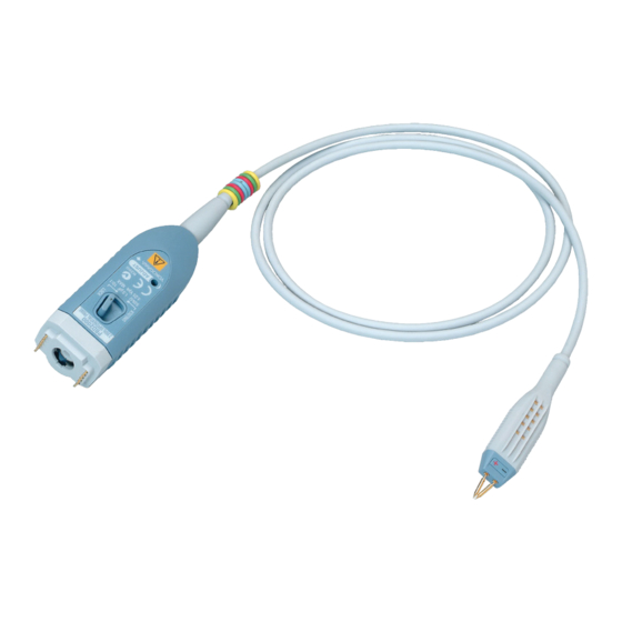
Component Names Cable Probe head Add various attachments, connect to circuit under test Probe interface To digital oscilloscope input Latch release lever Output terminal Variable resistor for adjusting offset voltage Probe head Cable Interface Probe interface spring pin Attachments L-pins (2) Lead wires (one each in red and black) Microclips Straight pins (8) -
Page 11: Usage Precautions
Component Names Output termina The output terminal is a BNC connector. It connects to an oscilloscope input BNC connector. Variable resistor for adjusting offset voltage You can adjust the offset voltage using an appropriate driver as described below. Adjustment driver Use an adjustment driver that fits into the adjustment groove. -
Page 12: Operating Procedures
Operating Procedures Preparation Have the probe and a digital oscilloscope with a probe interface ready. Insert the probe interface completely into the oscilloscope input, and confirm that the BNC connector and interface pin are securely fastened. You will hear the latch click when the connectors lock into place. Attach any of the provided attachments to the probe head signal input terminals. - Page 13 Example • For signals of relatively low frequency Lead wire Microclips • For signals of relatively high frequency Probe head Select an attachment according to the circuit to be tested (straight pin, angle pin, spring-type straight pin, or spring-type angle pin). IM 701923-01E...
- Page 14 Warm-up and Offset Adjustment Warm-up Immediately after connecting the probe, the heat emitted by the probe itself causes the offset voltage to drift. Warm up the probe for at least 30 minutes after applying power to stabilize the probe. Offset Adjustment You can turn the offset voltage adjustment variable resistor on the probe interface by using an appropriate adjustment driver (see page 3 for details) to adjust the residual offset voltage that remains even after warm-up.
-
Page 15: Product Specifications
Product Specifications Electrical Specifications (The electrical specifications are based on standard operating environment after 30-minute warm-up.) Frequency bandwidth DC to 2 GHz (–3 dB or higher) Attenuation ratio and DC 10:1, within ±2% of the differential input voltage (into voltage accuracy 50-Ω load, excluding oscilloscope errors) Input capacitance Approx. - Page 16 Product Specifications General Specifications Supply voltage range Interface Standard supply voltage ± 5V, within ±5% (Power is supplied to the probe through a dedicated terminal. Connect the probe to a digital oscilloscope with a compatible terminal.) Storage altitude 3000 m or less Operating altitude 2000 m or less Standard operating environment Temperature range 23 ±...
-
Page 17: Appendix-Probing
DC and low frequencies. Yokogawa’s standard 10:1 passive probes are easy-to-use for general applications. Their input impedance is 10 MΩ and approximately 14 pF in parallel, and the withstand voltage is 600 V. However, the 14 pF input capacitance might cause problems when high frequencies are measured. - Page 18 Appendix—Probing Active Probes and FET Probes Active and FET probes are those most often used to measure high frequency signals. Unlike passive probes, an impedance-converting buffer amplifier is situated near the tip of the probe which enables them to handle higher frequencies with around 1-pF input capacitance.
- Page 19 Appendix—Probing Problems with Probing High-Speed Signals Loading Effect When a probe is connected to the circuit under test, the input impedance of the probe itself has certain effects on the circuit. This is called the loading effect. There can be cases where there are notable low pass filter effects caused by the signal source impedance and the probe’s load capacitance, particularly when observing frequency components of 100 MHz or more.
- Page 20 Appendix—Probing Changes in Cable Characteristics A coaxial cable is used to transfer signals from the probe tip to the oscilloscope. Cables that can offer the right balance of both flexibility and high frequency performance are selected after considering the ways in which the cables will actually be handled.
- Page 21 Appendix—Probing Ringing Comparison When inductance is large and ringing can be seen When inductance is reduced and ringing is suppressed Probe Cable Bending Secure with tape or other means App-5 IM 701923-01E...
Need help?
Do you have a question about the PBD2000 and is the answer not in the manual?
Questions and answers