Table of Contents
Advertisement
Quick Links
GETTING STARTED GUIDE
NI 6585/6585B
Low-Voltage Differential Adapter Module
Note
Before you begin, complete the software and hardware installation
instructions in your FlexRIO FPGA getting started guide or controller for FlexRIO
getting started guide.
Caution
may impair the protection the NI 6585/6585B provides.
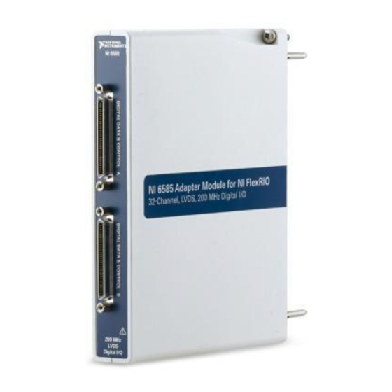
The NI 6585/6585B is a low-voltage differential (LVDS) adapter module designed to work in
conjunction with FlexRIO FPGA modules and controllers for FlexRIO.
This document explains how to install and configure the NI 6585/6585B.
Note
NI 6585R refers to the combination of your NI 6585/6585B adapter module
and either a FlexRIO FPGA module or a controller for FlexRIO. NI 6585/6585B
refers to your adapter module only.
Contents
Electromagnetic Compatibility Guidelines............................................................................... 1
FlexRIO Documentation........................................................................................................... 2
Verifying the System Requirements..........................................................................................4
Compatibility with FPGA Modules and Controllers for FlexRIO............................................4
Unpacking................................................................................................................................. 4
Preparing the Environment....................................................................................................... 5
Installing the NI 6585/6585B....................................................................................................5
Front Panel and Connector Pinouts...........................................................................................6
Pinout and Signal Information.......................................................................................... 7
Component-Level Intellectual Property (CLIP)......................................................................11
NI 6585/6585B CLIP...................................................................................................... 11
Worldwide Support and Services............................................................................................ 11
Where to Go Next................................................................................................................... 12
Electromagnetic Compatibility Guidelines
This product was tested and complies with the regulatory requirements and limits for
electromagnetic compatibility (EMC) stated in the product specifications. These requirements
and limits are designed to provide reasonable protection against harmful interference when the
product is operated in the intended operational electromagnetic environment.
Using the NI 6585/6585B in a manner not described in this document
Advertisement
Table of Contents

Related Manuals for National Instruments NI 6585


Summary of Contents for National Instruments NI 6585
-
Page 1: Table Of Contents
Using the NI 6585/6585B in a manner not described in this document may impair the protection the NI 6585/6585B provides. The NI 6585/6585B is a low-voltage differential (LVDS) adapter module designed to work in conjunction with FlexRIO FPGA modules and controllers for FlexRIO. -
Page 2: Flexrio Documentation
To ensure the specified EMC performance, the length of all I/O cables must be no longer than 30 m (100 ft). Caution Using the NI 6585/6585B in a manner not described in this document may impair the protection the NI 6585/6585B provides. FlexRIO Documentation Table 1. - Page 3 FlexRIO. IPNet Located at ni.com/ipnet. Contains LabVIEW FPGA functions and intellectual property to share. FlexRIO product page Located at ni.com/flexrio. Contains product information and data sheets for FlexRIO devices. NI 6585/6585B Getting Started Guide | © National Instruments | 3...
-
Page 4: Verifying The System Requirements
Verifying the System Requirements To use the NI 6585/6585B, your system must meet certain requirements. For more information about minimum system requirements, recommended system, and supported application development environments (ADEs), refer to the readme, which is available on the software media or online at ni.com/updates. -
Page 5: Preparing The Environment
Preparing the Environment Ensure that the environment you are using the NI 6585/6585B in meets the following specifications. 0 °C to 55 °C Operating temperature (IEC 60068-2-1, IEC 60068-2-2) Operating humidity (IEC 60068-2-56) 10% to 90% RH, noncondensing Pollution Degree Maximum altitude 2,000 m at 25 °C ambient temperature... -
Page 6: Front Panel And Connector Pinouts
Caution Connections that exceed any of the maximum ratings of any connector on the NI 6585/6585B can damage the device and the chassis. NI is not liable for any damage resulting from such connections. 6 | ni.com | NI 6585/6585B Getting Started Guide... -
Page 7: Pinout And Signal Information
Pinout and Signal Information The following table contains pin location and signal information for the NI 6585/6585B. Note DIO <0..15>+/-, PFI <0..4>+/-, and DDC CLOCK OUT appear on both connectors, DDCA and DDCB. Table 3. DDC Connector Pins Signal Name... - Page 8 34, 35, 36, 39, 42, 45, 48, 51, 54, 57, 60, 63, 66 The following table lists the NI 6585/6585B connector signals and corresponding FlexRIO FPGA module signals necessary for designing a custom CLIP. 8 | ni.com | NI 6585/6585B Getting Started Guide...
- Page 9 Table 4. NI 6585/6585B Connector Signals and FlexRIO FPGA Module Signals NI 6585/6585B FlexRIO FPGA Module Connector Signal Name GPIO Out GPIO Out GPIO In Enable DDCA GLOBAL CLOCK 0 — — GClk_SE DIO 0+/- GPIO_30_n GPIO_31 GPIO_31_n DIO 1+/-...
- Page 10 Table 5. NI 6585/6585B Connector Signals and FlexRIO FPGA Module Signals (Continued) NI 6585/6585B FlexRIO FPGA Module Connector Signal Name GPIO Out GPIO Out GPIO In Enable DDCB GLOBAL CLOCK 1 — — GClk_LVDS DIO 0+/- GPIO_46 GPIO_46_n GPIO_47 DIO 1+/-...
-
Page 11: Component-Level Intellectual Property (Clip)
(LVDS) channels using a simple channel-based interface. Each I/O line has a write enable signal. This CLIP provides a clock signal for export on each connector. The clock inputs from the NI 6585 are passed to LabVIEW FPGA for use in the FPGA VI. This CLIP also allows for individual clock output inversion. -
Page 12: Where To Go Next
Where to Go Next Refer to the following figure for information about other product tasks and associated resources for those tasks. 12 | ni.com | NI 6585/6585B Getting Started Guide... - Page 13 LabVIEW FPGA Development Kit Module Help User Manual DISCOVER more about your products through ni.com. Support FlexRIO Services ni.com/support ni.com/flexrio ni.com/services *This item is also installed with the driver software. NI 6585/6585B Getting Started Guide | © National Instruments | 13...
- Page 14 CONTAINED HEREIN AND SHALL NOT BE LIABLE FOR ANY ERRORS. U.S. Government Customers: The data contained in this manual was developed at private expense and is subject to the applicable limited rights and restricted data rights as set forth in FAR 52.227-14, DFAR 252.227-7014, and DFAR 252.227-7015. © 2015 National Instruments. All rights reserved. 375675A-01 Oct15...
Need help?
Do you have a question about the NI 6585 and is the answer not in the manual?
Questions and answers