
Related Manuals for Tektronix AWG4162


Summary of Contents for Tektronix AWG4162
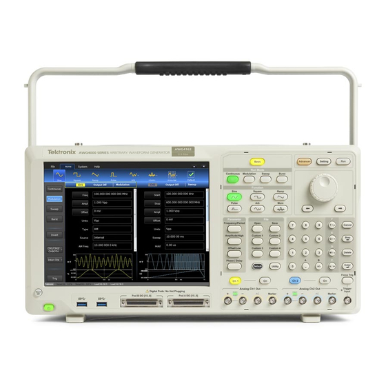
- Page 1 AWG4162 Arbitrary Waveform Generator Specifications and Performance Verification Technical Reference Rev C www.tek.com *P077119700* 077-1197-00...
- Page 2 Copyright © Tektronix. All rights reserved. Licensed software products are owned by Tektronix or its subsidiaries or suppliers, and are protected by national copyright laws and international treaty provisions. Tektronix products are covered by U.S. and foreign patents, issued and pending. Information in this publication supersedes that in all previously published material.
- Page 3 Warranty Tektronix warrants that the product will be free from defects in materials and workmanship for a period of three (3) years from the date of original purchase from an authorized Tektronix distributor. If the product proves defective during this warranty period, Tektronix, at its option, either will repair the defective product without charge for parts and labor, or will provide a replacement in exchange for the defective product.
-
Page 5: Table Of Contents
Required equipment ..................Basic mode: Frequency/Period test ................. Amplitude test....................DC Offset and Vocm tests..................Basic mode: AC Flatness test ................Basic mode: Harmonics distortion test ..............Basic mode: Spurious test ................... Test record ..................... AWG4162 Specifications and Performance Verification... - Page 6 Figure 8: 50 Ω terminator accuracy ................Figure 9: 1 kHz setup for AC Flatness test ..............Figure 10: >1 kHz setup for AC Flatness test ..............Figure 11: Harmonic distortion tests ................Figure 12: Spurious tests ..................AWG4162 Specifications and Performance Verification...
- Page 7 Table 32: Auxiliary ports: External sampling clock input ............ Table 33: Auxiliary ports: External modulation input ............Table 34: Power ....................Table 35: Environmental ..................Table 36: Physical characteristics ................Table 37: INIT and SYNCH error codes................ Table 38: Diagnostic error codes ................AWG4162 Specifications and Performance Verification...
- Page 8 Table of Contents Table 39: Required test equipment ................Table 40: AWG4162 Performance Test Record..............Table 41: Basic Mode Harmonic Distortion Test Record ............. AWG4162 Specifications and Performance Verification...
-
Page 9: Important Safety Information
See instructions for the location. Do not position the equipment so that it is difficult to operate the power cord; it must remain accessible to the user at all times to allow for quick disconnection if needed. AWG4162 Specifications and Performance Verification... - Page 10 Use only insulated voltage probes, test leads, and adapters supplied with the product, or indicated by Tektronix to be suitable for the product. Observe all terminal ratings. To avoid fire or shock hazard, observe all ratings and markings on the product.
-
Page 11: Service Safety Summary
Use care when lifting and carrying the product. This product is provided with handles for lifting and carrying. Use only the Tektronix rackmount hardware specified for this product. Keep product surfaces clean and dry. Remove the input signals before you clean the product. -
Page 12: Terms In This Manual
find out the nature of the potential hazards and any actions which have to be taken to avoid them. (This symbol may also be used to refer the user to ratings in the manual.) The following symbol(s) may appear on the product: viii AWG4162 Specifications and Performance Verification... -
Page 13: Service Safety Summary
Use Care When Servicing With Power On. Dangerous voltages or currents may exist in this product. Disconnect power, remove battery (if applicable), and disconnect test leads before removing protective panels, soldering, or replacing components. To avoid electric shock, do not touch exposed connections. AWG4162 Specifications and Performance Verification... - Page 14 Service Safety Summary AWG4162 Specifications and Performance Verification...
-
Page 15: Preface
Preface This manual provides product specifications and instructions to verify performance of the AWG4162 Arbitrary Waveform Generator. To prevent personal injury or damage to the instrument, consider the following before attempting service: The procedures in this manual should be performed only by a qualified service person. - Page 16 (such as a circuit board). Sometimes a single component is a module; for example, the chassis of the instrument is a module. Safety Symbols and terms related to safety appear in the Safety Summary near the beginning of this manual. AWG4162 Specifications and Performance Verification...
-
Page 17: Specifications
Includes allowances for Aging per Year, Reference Frequency Calibration Accuracy, and Temperature Stability. Aging Per Year: ±1.0 x 10 Reference oscillator calibration ±1.0 × 10 when operated within 25 °C ±5 °C, after 30 minute warm-up accuracy Reference oscillator aging Within ±1.0 x 10 /year AWG4162 Specifications and Performance Verification... -
Page 18: Table 2: Skew Control (Analog To Analog Skew)
In this mode, the sampling clock is fixed. Run mode Continuous, Modulation, Sweep, and Burst Burst count 1 to 1,000,000 cycles or infinite Internal trigger delay 0 to 100 s Resolution: 1 ps, 15 digits AWG4162 Specifications and Performance Verification... -
Page 19: Table 6: Waveforms (Basic Mode), Nominal
Sine, Square, Pulse, Ramp, More (Sin(x)/x, Noise, DC, Gaussian, Lorentz, Exponential Rise, Exponential Decay, and Haversine) Arbitrary waveform User defined waveforms. Users can edit and save their own waveforms. Waveform length 16384/Channel Sampling rate 2.5 GS/s Resolution 14 bits AWG4162 Specifications and Performance Verification... -
Page 20: Table 7: Analog Output (Basic Mode), Frequency/Period
50 Ω load, single ended –2.5 V to +2.5 V High Z load, single –5 V to +5 V ended Resolution 1 mV or 4 digits Accuracy 50 Ω load, single ended: 1% of │setting│+5 mV AWG4162 Specifications and Performance Verification... -
Page 21: Table 8: Analog Output (Basic Mode), Amplitude
50 Ω load, single ended –2.5 V to +2.5 V High Z load, single –5 V to +5 V ended Resolution 1 mV or 4 digits Accuracy 50 Ω load, single ended: 1% of │setting│+5 mV AWG4162 Specifications and Performance Verification... -
Page 22: Table 10: Analog Output (Basic Mode), Offset
High Z load, single 1 μHz to 350 MHz: –10 V to +10 V ended 350 MHz to 550 MHz: –8 V to +8 V 550 MHz to 600 MHz: –7 V to +7 V AWG4162 Specifications and Performance Verification... -
Page 23: Table 12: Analog Output (Basic Mode), Sine Wave
Leading/Trailing Edge Transition Time At 10% to 90% of amplitude for leading time: 800 ps to 1000 s Resolution: 1 ps or 15 digits Overshoot, typical < –2% at 1 Vpp Jitter (rms), typical 50 ps AWG4162 Specifications and Performance Verification... -
Page 24: Table 15: Ramp
(For FSK, PSK only) External: Max 10 MHz Amplitude modulation (AM) Depth 0.00% to +120.00% Frequency modulation (FM) Peak deviation DC to 300 MHz Phase modulation (PM) Phase deviation range 0.00 to +180.00 degrees Frequency Shift Keying (FSK) AWG4162 Specifications and Performance Verification... -
Page 25: Table 19: Sweep
It is a sophisticated playback system that delivers waveforms based on stored digital data that describes the constantly changing voltage levels of an AC signal. In this mode, the sampling clock is variable. Run mode Continuous, Sequence, Triggered, Gated AWG4162 Specifications and Performance Verification... -
Page 26: Table 22: Advanced Run Mode
Table 23: Waveforms (Advanced mode), nominal Characteristic Description Standard Analog waveforms DC, Sine, Cosine, Triangle, Rectangle, Sawtooth, Increase-ramp, Decrease-ramp, Pulse, Sinc, Exponential, Sweep Arbitrary Formula, file, user defined Additional Noise and Filter can be applied to the waveforms above AWG4162 Specifications and Performance Verification... -
Page 27: Table 24: Analog Output Of Advanced Mode (Amp/Direct Dac/Ac)
Output relay is available for each channel. A control is common to the complementary output. Skew between (+) and (–) Less than 20 ps, when in Direct output mode; Normal mode output, typical Bandwidth Calculated bandwidth, typical AMP: 400 MHz Direct DAC: 750 MHz AC: 750 MHz Amplitude AWG4162 Specifications and Performance Verification... - Page 28 AMP: –2.50 V - + 2.50 V Direct DAC: –0.35 V - + 0.35 V In the case of differential output or high Z load, the amplitude is twice that of single ended with 50 Ω load. AWG4162 Specifications and Performance Verification...
- Page 29 AMP: At amplitude 1.0 Vpp , relative to 100 kHz; AMP mode is LPF ON DAC: At amplitude 0.5 Vpp , relative to 100 kHz AC: At amplitude 1.0 Vpp , relative to 10 MHz AWG4162 Specifications and Performance Verification...
- Page 30 39.0625 MHz AMP: –115 dBc/Hz Direct DAC: –115 dBc/Hz AC: –115 dBc/Hz 78.125 MHz AMP: –110 dBc/Hz Direct DAC: –110 dBc/Hz AC: –110 dBc/Hz 156.25 MHz AMP: –105 dBc/Hz Direct DAC: –105 dBc/Hz AC: –105 dBc/Hz AWG4162 Specifications and Performance Verification...
-
Page 31: Table 25: Auxiliary Ports: Marker Output
<800 ps (10% to 90% of swing), when Hi = 2.5 V, Low = 0 V Total jitter on random pattern, typical 155 ps peak-peak (PN15 Pattern, when Hi = 2.5 V, Low = 0 V) (Measured at bit error rate = 1e AWG4162 Specifications and Performance Verification... -
Page 32: Table 26: Auxiliary Ports: Trigger/Gate Input
Arb mode 16 Ch: 1.25 Gbps Arb mode 32 Ch: 625 Mbps Table 28: Auxiliary ports: Memory depth (Digital output (with option)) Analog memory depth 0.5M Arb mode 16 Ch Arb mode 32 Ch 0.25M AWG4162 Specifications and Performance Verification... -
Page 33: Table 29: Auxiliary Ports: Sync In/Out
50 Ω, AC coupled Number of inputs 2, one for each input Frequency range 1.25 GHz to 2.5 GHz Input voltage range -5 dBm to 4 dBm Damage level: +8 dBm max Damage level: ±15 V DC max AWG4162 Specifications and Performance Verification... -
Page 34: General Specifications
Up to 3,000 meters (9,843 feet) Non operating Up to 12,000 meters (39,370 feet) Table 36: Physical characteristics Characteristic Description Net weight, typical 6.5 kg (14.2 lbs) Net weight with packaging, typical 11.5 kg (25.2 lbs) AWG4162 Specifications and Performance Verification... - Page 35 Height: 233 mm (9.173 in) Width: 439 mm (17.283 in) Depth: 199 mm (7.835 in) Clearance required for cooling 50.8 mm (2.0 in) Left side (when looking at the front of the instrument) and rear. AWG4162 Specifications and Performance Verification...
- Page 36 Specifications AWG4162 Specifications and Performance Verification...
-
Page 37: Performance Verification
°C and +50 °C. Performance conditions In addition to the above requirements, all of the performance tests in this section comprise an extensive, valid confirmation of performance and functionality when the following additional requirement is met: AWG4162 Specifications and Performance Verification... -
Page 38: Self Tests
3. Select System > Tools > Warm up Timer. 4. After the 30 minutes of warm up time, press or click the Self Calibration button to start the test. 5. Wait until the test is complete. AWG4162 Specifications and Performance Verification... -
Page 39: Error Codes
CHECK_DEVICE_DATA 1301010 GET_SERIAL_NUMBER 1301020 GET_DEVICE_MODEL 1301030 GET_MEMORY_OPTION 1301040 GET_DIGITAL_OPTION 1301050 LOAD_CONTROL_FPGA_FIRMWARE 1301060 RESET_RELAIS 1301070 CHECK_DEVICE_MODEL 1301080 SET_REFERENCE_CLOCK 1301090 LTC2265_INITIALIZATION 1301100 AD5390_RESET 1301110 AD5390_SET_REFERENCE 1301120 TRIGGER_INITIALIZATION 1301130 SET_MARKER_LEVEL 1301140 READ_FREQUENCY_TUNING_PARAMETER 1301150 SET_FREQUENCY_TUNING 1301160 CREATE_CHANNEL_DATA 1301170 CREATE_CHANNEL AWG4162 Specifications and Performance Verification... - Page 40 RESET_VOCM_DC_DIRECT_CHANNEL A 1302221 RESET_VOCM_DC_AMP_CHANNEL A 1302231 GET_FPGA_VERSION_CHANNEL A 1302241 SET_FILTER_PARAMETER_CHANNEL A 1302251 RESET_ATTENUATOR_CHANNEL A 1302261 CHECK_DIGITAL_POD_CONNECTION_CHANNEL A 1302271 SET_DIGITAL_POD_LEVEL_CHANNEL A 1302281 GET_IDENTIFIER_CHANNEL A 1302291 SET_SIGNAL_POLARITY_CHANNEL A 1302301 GET_FUNCTIONALITY_CHANNEL A 1302311 CHECK_FUNCTIONALITY_CHANNEL A 1302321 EXTERNAL_MODULATION_CALIBRATION_CHANNEL A AWG4162 Specifications and Performance Verification...
- Page 41 1302242 SET_FILTER_PARAMETER_CHANNEL B 1302252 RESET_ATTENUATOR_CHANNEL B 1302262 CHECK_DIGITAL_POD_CONNECTION_CHANNEL B 1302272 SET_DIGITAL_POD_LEVEL_CHANNEL B 1302282 GET_IDENTIFIER_CHANNEL B 1302292 SET_SIGNAL_POLARITY_CHANNEL B 1302302 GET_FUNCTIONALITY_CHANNEL B 1302312 CHECK_FUNCTIONALITY_CHANNEL B 1302322 EXTERNAL_MODULATION_CALIBRATION_CHANNEL B 1003000 CHECK_SYNCHRONIZATION_DATA 1003010 SET_DCO_DAC_DIVISOR 1003020 ACTIVATE_SYNCHRONIZATION 1003030 GET_CHANNEL_FPGA_TEMPERATURE AWG4162 Specifications and Performance Verification...
-
Page 42: Table 38: Diagnostic Error Codes
Step description 1400000 TEST_USB_CONNECTION FAILED 1401000 TEST_NVMEMORY_ACCESS FAILED 1402000 TEST_LOAD_CONTROL_FPGA_FW FAILED 1403000 TEST_CONTROL_FPGA_REGISTRY_ACCESS FAILED 1404000 TEST_I2C_EPROM FAILED 1405000 TEST_LOAD_CHANNEL_FPGA_DIAGNOSTIC_FW FAILED_CHANNEL_A 1405010 TEST_CHANNEL_FPGA_REGISTRY_ACCESS FAILED_CHANNEL_A 1405020 TEST_CHANNEL_MEMORY FAILED_CHANNEL_A 1405030 TEST_CHANNEL_SPI_DAC_9739 FAILED_CHANNEL_A 1405040 TEST_CHANNEL_ADC_LTC2265_COMMUNICATION FAILED_CHANNEL_A 1406000 TEST_LOAD_CHANNEL_FPGA_DIAGNOSTIC_FW FAILED_CHANNEL_B AWG4162 Specifications and Performance Verification... - Page 43 1408082 TEST_CHANNEL_OFFSET_DC_DIRECT FAILED_CHANNEL_A_BRANCH_P 1408092 TEST_CHANNEL_VOCM_DC_DIRECT FAILED_CHANNEL_A_BRANCH_P 1408102 TEST_CHANNEL_VAO_DC_DIRECT FAILED_CHANNEL_A_BRANCH_P 1408112 TEST_CHANNEL_ATTENUATOR FAILED_CHANNEL_A_BRANCH_P 1409000 TEST_CHANNEL_ADC_LTC2265 FAILED_CHANNEL_B 1409010 TEST_CHANNEL_PLL FAILED_CHANNEL_B 1409020 TEST_CHANNEL_ADF4351 FAILED_CHANNEL_B 1409031 TEST_CHANNEL_OFFSET_DC_AMP FAILED_CHANNEL_B_BRANCH_N 1409041 TEST_CHANNEL_VOCM_DC_AMP FAILED_CHANNEL_B_BRANCH_N 1409051 TEST_CHANNEL_VAO_DC_AMP FAILED_CHANNEL_B_BRANCH_N 1409061 TEST_CHANNEL_OFFSET_GAIN_DC_AMP_FAILED_CHANNEL_B_BRANCH_N 1409071 TEST_CHANNEL_DIFFERENTIAL_OFFSET_DC_DIRECT FAILED_CHANNEL_B_BRANCH_N AWG4162 Specifications and Performance Verification...
-
Page 44: Required Equipment
Checks clock frequency. measurement Oscilloscope 4 GHz Bandwidth 50 Ω input. Tektronix MSO70804C Checks output signals. Used in Termination 25 GS/s multiple procedures. Spectrum analyzer 20 kHz to 6 GHz Tektronix RSA5106B Checks output signals. Harmonics Spurious. AWG4162 Specifications and Performance Verification... -
Page 45: Basic Mode: Frequency/Period Test
Operation Function Sine Sine (front) Frequency 1.000000 MHz Frequency/Period (front) Amplitude 1.00 Vpp Amplitude/High (front) Channel 1 Output On (front) 4. Check that reading of the frequency counter is between 0.9999984 MHz and 1.0000016 MHz. AWG4162 Specifications and Performance Verification... -
Page 46: Amplitude Test
0.9962 (= 2 / (1 + 50 / 49.62)) 3. Connect the generator to the DMM as shown in the following figure. Be sure to connect the 50 Ω terminator to the generator’s side output connector. Figure 3: Amplitude test, Basic mode AWG4162 Specifications and Performance Verification... -
Page 47: Figure 4: Amplitude Test, Advanced Mode
3. Set up the generator using the following steps: Select menu Setting Operation New waveform Sine, 64k points Home > ArbBuilder> New Std Set Function to Sine and Total Number of Points to 64 Sampling rate 64 MS/s Setting/Timing AWG4162 Specifications and Performance Verification... -
Page 48: Dc Offset And Vocm Tests
(1 + 50 / Measurement Ω Ω) Measurement (reading of the DMM) Ω Examples 50.50 Ω 1.0050 (= 2 / (1 + 50 / 50.50)) 49.62 Ω 0.9962 (= 2 / (1 + 50 / 49.62)) AWG4162 Specifications and Performance Verification... -
Page 49: Figure 6: Dc Offset/Vocm Tests, Basic Mode
9. Verify that each Vocm measurement is within the range specified in the test record. 10. Record the results in the test record. 11. Repeat steps 8 through 10 for the CH1–, CH2+, and CH2– outputs. AWG4162 Specifications and Performance Verification... -
Page 50: Figure 7: Dc Offset/Vocm Test, Advanced Mode
Set up the generator using the following steps: Select menu Setting Operation Function Vocm Quick Settings menu Vocm Quick Settings menu Channel 1 Output DC direct: +0.350 V On (front) DC amplified: +2.500 V AWG4162 Specifications and Performance Verification... -
Page 51: Basic Mode: Ac Flatness Test
3. Connect the generator to the DMM as shown in the following figure. Be sure to connect the 50 Ω terminator to the generator’s side output connector. Figure 9: 1 kHz setup for AC Flatness test AWG4162 Specifications and Performance Verification... -
Page 52: Figure 10: >1 Khz Setup For Ac Flatness Test
6. Repeat steps 3 through 5 with the generator set to each of the other frequencies specified in the test record tables. 7. Repeat this procedure starting at step 3 of the 1 kHz test setup for the CH1–, CH2+, and CH2– outputs. AWG4162 Specifications and Performance Verification... -
Page 53: Basic Mode: Harmonics Distortion Test
7. Verify that the differences between the reference level and the signal level in the frequency of higher-order at each frequency are below the limit specified in the following tables. 8. Repeat steps 2 through 4 for the CH1–, CH2+, and CH2– outputs. AWG4162 Specifications and Performance Verification... -
Page 54: Basic Mode: Spurious Test
8. Verify that the spurious signal at each frequency is equal to or less than the limit specified in the following tables. 9. Record the results in the test record. 10. Repeat steps 2 through 9 for the CH1–, CH2+, and CH2– outputs. AWG4162 Specifications and Performance Verification... -
Page 55: Test Record
Performance verification Test record Photocopy the test records and use them to record the performance test results for your AWG4162 Arbitrary Waveform Generator. AWG4162 Specifications and Performance Verification... - Page 56 Performance verification Table 40: AWG4162 Performance Test Record Instrument Serial Number: Certificate Number: Temperature: RH %: Date of Calibration: Technician: Basic mode Frequency Test Record Minimum Test result Maximum Frequency Sine at 1.000000 MHz 0.9999984 MHz 1.0000016 MHz Sine at 1.000000 MHz 0.9999984 MHz...
- Page 57 400 mVpp: 141.4 mVrms (141.4 × CF - 3.182) mVrms (141.4 × CF +3.182) mVrms at 1.00 kHz 800 mVpp: 282.9 mVrms (282.9 × CF - 4.597) mVrms (282.9 × CF +4.597) mVrms at 1.00 kHz AWG4162 Specifications and Performance Verification...
- Page 58 +2.50 Vdc (+2.50 × CF - 0.03) Vdc (+2.50 × CF + 0.03 Vdc 0.00 Vdc -5.00 mVdc +5.00 mVdc -2.50 Vdc (-2.50 × CF - 0.03) Vdc (-2.50 × CF + 0.03) Vdc CH1– offset AWG4162 Specifications and Performance Verification...
- Page 59 CH1+ offset +2.50 Vdc (+2.50 × CF - 0.03) Vdc (+2.50 × CF + 0.03) Vdc 0.00 Vdc -5.00 mVdc +5.00 mVdc -2.50 Vdc (-2.50 × CF - 0.03) Vdc (-2.50 × CF + 0.03) Vdc AWG4162 Specifications and Performance Verification...
- Page 60 CF = 2 / (1 + 50 Ω / Measurement Ω) = CH1+ offset Minimum Test result Maximum +0.35 Vdc (+0.35 × CF - 0.0085) Vdc (+0.35 × CF + 0.0085) Vdc 0.00 Vdc -5.00 mVdc +5.00 mVdc AWG4162 Specifications and Performance Verification...
- Page 61 Maximum ———- ———- Frequency 1.00 kHz dB ( = Reference) (Ampl: +1 Vpp) Frequency 500 kHz Reference - 0.5 dB Reference + 0.5 dB Frequency 1.00 MHz Reference - 0.5 dB Reference + 0.5 dB AWG4162 Specifications and Performance Verification...
- Page 62 Reference + 0.50 dB Frequency 150.00 MHz Reference - 0.5 dB Reference + 0.50 dB Frequency 200.00 MHz Reference - 0.5 dB Reference + 0.50 dB Frequency 300.00 MHz Reference - 0.5 dB Reference + 0.50 dB AWG4162 Specifications and Performance Verification...
- Page 63 -60 dBc (dBc) CH1– Harmonic Distortion (dBc) reading - 0 dBc Nth - reference < reference -60 dBc (dBc) Sine 100 MHz 100 MHz 200 MHz 300 MHz 400 MHz 500 MHz CH1+ Harmonic Distortion (dBc) AWG4162 Specifications and Performance Verification...
- Page 64 20 MHz 25 MHz CH2+ Harmonic Distortion (dBc) reading - 0 dBc Nth - reference < reference -60 dBc (dBc) CH2– Harmonic Distortion (dBc) reading - 0 dBc Nth - reference < reference -60 dBc (dBc) AWG4162 Specifications and Performance Verification...
- Page 65 2400 MHz 3 GHz CH2+ Harmonic Distortion (dBc) reading - 0 dBc Nth - reference < reference -28 dBc (dBc) CH2– Harmonic Distortion (dBc) reading - 0 dBc Nth - reference < reference -28 dBc (dBc) AWG4162 Specifications and Performance Verification...
- Page 66 20 MHz / 20 kHz / < -50 dBc 625 MHz 1250 MHz 20 kHz < -40 dBc Sine 600 MHz 10 MHz / 20 MHz / 20 kHz / 625 MHz 1250 MHz 20 kHz AWG4162 Specifications and Performance Verification...
Need help?
Do you have a question about the AWG4162 and is the answer not in the manual?
Questions and answers