Table of Contents
Advertisement
Quick Links
Advertisement
Table of Contents

Related Manuals for TEDIA PCD-8006


Summary of Contents for TEDIA PCD-8006
- Page 1 Digital I/O PCIe card PCD-8006 User Guide...
- Page 2 “as is,” without warranty of any kind, either expressed or ® implied, including, but not limited to, its particular purpose. TEDIA reserves the right to make improvements and/or changes to this manual, or to the products and/or the programs described in this manual, at any time.
- Page 3 PCD-8006 User Guide - Table of Contents Table of Contents CE Declaration of Conformity, WEEE 1. Introduction Description ...........
-
Page 4: Ce Declaration Of Conformity
PCD-8006 User Guide - CE Declaration of Conformity, WEEE CE Declaration of Conformity ® All TEDIA products described in this user guide comply with the essential requirements of the following applicable European Directives: • Electromagnetic Compatibility (EMC) Directive 2014/30/EU • RoHS Directive (EU) 2015/863 amending Annex II to... - Page 5 General instructions for use The PCD-8006 card is suitable for installation in either office or industrial computers that are fitted with the PCI Express bus (Gen 1 compatible). Cable types and their maximum length are described in paragraph 2.3 General data.
-
Page 6: Specifications
PCD-8006 User Guide Specifications Digital ports Number of ports: six 8-bit bidirectional ports Operating levels: HC/HCT/TTL Load impedance of outputs: 500 Ohm min. Note: Digital bidirectional ports are not protected against overvoltage, stresses outside the range 0÷5 V will may cause permanent damage. -
Page 7: Installation
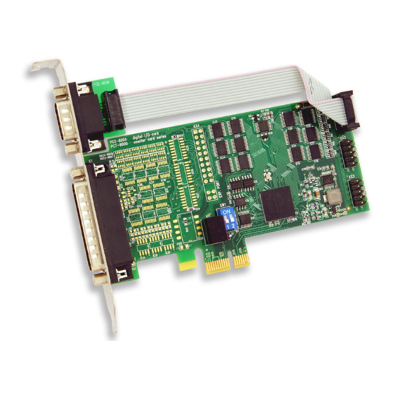
For further information see manufacturer's website http://www.tedia.eu. Hardware configuration The PCD-8006 card contains a single configuration element - a two-segment DIP switch (the status of this switch can be read by the program to identify multiple cards as CardID value). -
Page 8: Digital Ports
(ie. DIO3, DIO4 and DIO5) use header type connectors located at the back edge of the card. In case of the standard format card (ie. PCD-8006), the DIO3 port is accessed on the card bracket via adapter cable PCE-8019 terminated with D-Sub 9 connector. Remaining two ports (ie. - Page 9 PCD-8006 User guide - Appendix, Tables and Figures PCD-8006 PCE-8019 Card ID ID=0 ID=1 ID=2 ID=3 PCD-8006/LP Card ID ID=0 ID=1 ID=2 ID=3 Figure 1. Location of switches and connectors on both version of card. connector of digital ports DIO0÷DIO2, ie. DIO00÷DIO23 signals (D-Sub 25 - male) connector of digital port DIO3, ie.
- Page 10 PCD-8006 User guide - Appendix, Tables and Figures K1 signal (PCE-8025/LP) K1 signal (PCE-8025/LP) DIO0 (DIO24) DIO1 (DIO25) DIO2 (DIO26) DIO3 (DIO27) DIO4 (DIO28) DIO5 (DIO29) DIO6 (DIO30) DIO7 (DIO31) DIO8 (DIO32) DIO9 (DIO33) DIO10 (DIO34) DIO11 (DIO35) DIO12 (DIO36)
- Page 11 PCD-8006 User guide - Appendix, Tables and Figures Figure 2. Pin layout on D-Sub 25 (male), D-Sub 9 (male) and header type connectors (2x 5 pins, 2.54 mm pitch). INPUT mode of DIO port PCIe card DIOxx DIOxx data data...
- Page 12 PCD-8006 User Guide - Notes ........................................................................................................................................................................................................................................................................................................................................................................................................................................................................................................................................................................................................................................................................................................................................................................................................
Need help?
Do you have a question about the PCD-8006 and is the answer not in the manual?
Questions and answers