Table of Contents
Advertisement
Quick Links
Advertisement
Table of Contents

Related Manuals for SIM Tech SimCom SIM340


Summary of Contents for SIM Tech SimCom SIM340
- Page 1 Hardware Design SIM340_HD_V3.09...
- Page 2 SIM340 Hardware Design SIM340 Hardware Design Document Title: 3.09 Version: 2009-3-18 Date: Release Status: SIM340_HD_V3.09 Document Control ID: General Notes SIMCom offers this information as a service to its customers, to support application and engineering efforts that use the products designed by SIMCom. The information provided is based upon requirements specifically provided to SIMCom by the customers.
-
Page 3: Table Of Contents
SIM340 Hardware Design Contents Contents ............................3 Version history..........................7 1 Introduction............................9 1.1 Related documents .......................9 1.2 Terms and abbreviations.....................10 2 SIM340 overview.........................13 2.1 SIM340 key features ......................14 2.2 SIM340 functional diagram ....................15 2.3 SIM340 evaluation board ....................16 3 Application interface........................18 3.1 SIM340 pin description......................18 3.2 Operating modes ........................21 3.3 Power supply........................22 3.3.1 Power supply pins on the board-to-board connector ..........24... - Page 4 SIM340 Hardware Design 3.14 ADC ..........................49 3.15 Behaviors of the RI ......................50 3.16 Network status indication....................51 3.17 General purpose input & output (GPIO) ................52 4 Antenna interface .........................53 4.1 Antenna installation......................53 4.1.1 Antenna connector....................53 4.1.2 Antenna pad......................53 Module RF output power ......................53 4.2 Module RF receive sensitivity....................54 4.3 Module operating frequencies....................54 5 Electrical, reliability and radio characteristics ................55...
- Page 5 SIM340 Hardware Design Table Index TABLE 1: RELATED DOCUMENTS.....................9 TABLE 2: TERMS AND ABBREVIATIONS ..................10 TABLE 3: SIM340 KEY FEATURES....................14 TABLE 4: CODING SCHEMES AND MAXIMUM NET DATA RATES OVER AIR INTERFACE..15 TABLE 5: BOARD-TO-BOARD CONNECTOR PIN DESCRIPTION ..........18 TABLE 6: OVERVIEW OF OPERATING MODES................21 TABLE 7: AT COMMANDS USED IN ALARM MODE ..............27 TABLE 8: SUMMARY OF STATE TRANSITIONS................31 TABLE 9: PIN DEFINITION OF THE SERIAL INTERFACES ............35...
- Page 6 SIM340 Hardware Design Figure Index FIGURE 1: SIM340 FUNCTIONAL DIAGRAM .................16 FIGURE 2: TOP VIEW OF SIM300 EVB .....................17 FIGURE 3: REFERENCE CIRCUIT OF THE VBAT INPUT ..............23 FIGURE 4: REFERENCE CIRCUIT OF THE SOURCE POWER SUPPLY INPUT......23 FIGURE 5: VBAT VOLTAGE DROP DURING TRANSMIT BURST ..........24 FIGURE 6: TURN ON SIM340 USING DRIVING CIRCUIT .............25 FIGURE 7: TURN ON SIM340 USING BUTTON................25 FIGURE 8: TIMING OF TURN ON SYSTEM ..................26...
-
Page 7: Version History
SIM340 Hardware Design Version history Date Version Description of change Author 2005-04-13 01.00 Origin anthony 2005-06-29 01.01 Modify the RESET pin DC characteristics etc anthony 2005-08-02 01.02 Modify the ESD characteristics etc anthony 2005-08-23 01.03 Delete reset part, update mechanical dimensions, sleep anthony mode and board-to-board connector description 2005-11-02... - Page 8 SIM340 Hardware Design Modify the overview of operating modes Modify the MIC input characteristics Modify the BUZZER & NETLIGHT reference circuit Add the note in the chapter of the Serial Interfaces about RTS connected to GND 2007-07-31 03.06 Modify the current of VDD_EXT to 10mA. Modify the range of autobauding as 4800-115200bps.
-
Page 9: Introduction
SIM340 Hardware Design 1 Introduction This document describes the hardware interface of the SIMCom SIM340 module that connects to the specific application and the air interface. As SIM340 can be integrated with a wide range of applications, all functional components of SIM340 are described in great detail. -
Page 10: Terms And Abbreviations
SIM340 Hardware Design 1.2 Terms and abbreviations Table 2 : Terms and abbreviations Abbreviation Description Analog-to-Digital Converter Antenna Reference Point ASIC Application Specific Integrated Circuit Bit Error Rate Base Transceiver Station CHAP Challenge Handshake Authentication Protocol Coding Scheme Circuit Switched Data Clear to Send Digital-to-Analog Converter Discontinuous Reception... - Page 11 SIM340 Hardware Design Abbreviation Description Light Emitting Diode Li-Ion Lithium-Ion Mobile Originated Mobile Station (GSM engine), also referred to as TE Mobile Terminated Password Authentication Protocol PBCCH Packet Switched Broadcast Control Channel Printed Circuit Board Personal Communication System, also referred to as GSM 1900 Protocol Data Unit Point-to-point protocol Radio Frequency...
- Page 12 SIM340 Hardware Design Phonebook abbreviations Abbreviation Description SIM fix dialing phonebook SIM last dialing phonebook (list of numbers most recently dialed) Mobile Equipment list of unanswered MT calls (missed calls) SIM (or ME) own numbers (MSISDNs) list Mobile Equipment list of received calls SIM phonebook Not connect SIM340_HD_V3.09...
-
Page 13: Sim340 Overview
SIM340 Hardware Design 2 SIM340 overview Designed for global market, SIM340 is a Quad –band GSM/GPRS engine that works on frequencies GSM 850 MHZ, EGSM 900 MHz, DCS 1800 MHz and PCS 1900 MHz. SIM340 features GPRS multi-slot class 10/ class 8 (optional) and supports the GPRS coding schemes CS-1, CS-2, CS-3 and CS-4. -
Page 14: Sim340 Key Features
SIM340 Hardware Design 2.1 SIM340 key features Table 3 : SIM340 key features Feature Implementation Power supply Single supply voltage 3.4V – 4.5V Power saving Typical power consumption in SLEEP mode to 2.5mA ( BS-PA-MFRMS=5 ) Frequency Bands SIM340 Quad-band: GSM 850, EGSM 900, DCS 1800, PCS 1900. The SIM340 can search the 4 frequency bands automatically. -
Page 15: Sim340 Functional Diagram
SIM340 Hardware Design Debug port Serial Port can be used for CSD FAX, GPRS service and send AT command of controlling module. Serial Port can use multiplexing function. Autobauding supports baud rate from 4800 bps to 115200bps. Debug Port: Two lines on Serial Port Interface /TXD and /RXD Debug Port only used for debugging Phonebook management Support phonebook types: SM, FD, LD, RC, ON, MC. -
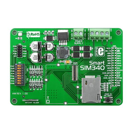
Page 16: Sim340 Evaluation Board
SIM340 Hardware Design SIM340 Antenna connector Radio Frequency POWER KEYPADS Flash+ Baseband SRAM Engine UART GPIO AUDIO Figure 2: SIM340 functional diagram 2.3 SIM340 evaluation board In order to help you on the application of SIM340 application, SIMCom can supply an Evaluation Board (EVB) that interfaces the SIM340 directly with appropriate power supply, SIM card holder, RS232 serial port, handset port, earphone port, antenna and all GPIO of the SIM340. - Page 17 SIM340 Hardware Design Figure 3: Top view of SIM300 EVB For details please refer to the SIM300-EVB_UGD document. SIM340_HD_V3.09 18.03.2009...
-
Page 18: Application Interface
SIM340 Hardware Design 3 Application interface SIM340 is equipped with a 60-pin 0.5mm pitch board-to-board connector that connects to the cellular application platform. Sub-interfaces included in this board-to-board connector are described in detail in following chapters: Power supply (please refer to Chapter 3.3) Serial interfaces (please refer to Chapter... - Page 19 SIM340 Hardware Design Otherwise, the system is power on. Digital ground Power on or power off PIN NAME DESCRIPTION DC CHARACTERISTICS PWRKEY Voltage input PWRKEY. VILmax=0.2*VBAT pull PWRKEY should be pulled low to VIHmin=0.6*VBAT VBAT power on or power off the system. VImax=VBAT The user should keep pressing the key for a moment when power on...
- Page 20 SIM340 Hardware Design keep pins DISP_CLK O/4mA open DISP_CS O/4mA DISP_D/C O/4mA DISP_RST O/4mA NETLIGHT O/4mA Network status indication unused keep pins GPIO0 I/O/4m Normal input/output port open Serial port PIN NAME DESCRIPTION DC CHARACTERISTICS I/8mA Data terminal ready VILmin=0V VILmax=0.3*VDD_EXT I/8mA Receive data...
-
Page 21: Operating Modes
SIM340 Hardware Design by software automatically SIM interface either 1.8V or 3V are protected SIM_DATA I/O/4m SIM data output VILmin=0V against VILmax=0.3*SIM_VDD with a TVS VIHmin=0.7*SIM_VDD diode array. SIM_CLK O/4mA SIM clock VIHmax= SIM_VDD+0.3 Maximum SIM_RST O/4mA SIM reset VOLmin=GND cable length VOLmax=0.2V... -
Page 22: Power Supply
SIM340 Hardware Design GPRS Module is ready for GPRS data transfer, but no data is STANDBY currently sent or received. In this case, power consumption depends on network settings and GPRS configuration. GPRS DATA There is GPRS data in transfer (PPP or TCP or UDP). In this case, power consumption is related with network settings (e.g. - Page 23 SIM340 Hardware Design Figure 4: Reference circuit of the VBAT input The circuit design of the power supply depends strongly from the power source where this power is drained. The following figure is the reference design of +5V input source power supply. The designed output for the power supply is 4V, thus a linear regulator can be used.
-
Page 24: Power Supply Pins On The Board-To-Board Connector
SIM340 Hardware Design 577us 4.615ms Burst:2A VBAT VBAT Max:400mV Figure 6: VBAT voltage drop during transmit burst 3.3.1 Power supply pins on the board-to-board connector Eight VBAT pins of the board-to-board connector are dedicated to connect the supply voltage; six GND pins are recommended for grounding. VRTC pin can be used to back up the RTC. 3.3.2 Minimizing power losses Please pay special attention to the supply power when you are designing your applications. - Page 25 SIM340 Hardware Design Via RTC interrupt: starts ALARM modes (please refer to chapter 3.4.1.2) Note: The AT command must be set after the SIM340 is power on and Unsolicited Result Code “RDY” is received from the serial port. However, if the SIM340 was set autobauding, the serial port will received nothing, the AT command can be set after 2-3s from the SIM340 is power on.
- Page 26 SIM340 Hardware Design VBAT Pulldown > 2s PWRKEY > 0.6*VBAT (INPUT) <0.2*VBAT VDD_EXT (OUTPUT) Figure 9: Timing of turn on system When power on procedure complete, the SIM340 will send out following result code to indicate the module is ready to operate when set as fixed baud rate. This result code does not appear when autobauding is active.
-
Page 27: Turn Off Sim340
SIM340 Hardware Design will return 0 which indicates that the protocol stack is closed. Then after 90s, SIM340 will power down automatically. However, during alarm mode, if the software protocol is started by AT+CFUN=1 command, the process of automatic power down will not be available. In alarm mode, driving the PWRKEY to a low level voltage for a period will cause SIM340 to be powered down (Please refer to the power down scenario). - Page 28 SIM340 Hardware Design Logout net about 2s to 8s 1s > Pulldown >0.5s PWRKEY (INPUT) >0.6*VBAT <0.2*VBAT VDD_EXT (OUTPUT) Figure 10: Timing of turn off system 3.4.2.2 Turn off SIM340 using AT command You can use an AT command “AT+CPOWD=1” to turn off the module. This command will let the module to log off from the network and allow the module to enter into a secure state and save data before completely disconnecting the power supply.
-
Page 29: Restart Sim340 Using The Pwrkey Pin
SIM340 Hardware Design If the voltage ≤ 3.4V, the following URC will be presented: UNDER-VOLTAGE POWER DOWN If the voltage ≥ 4.6V, the following URC will be presented: OVER-VOLTAGE POWER DOWN After this moment, no further more AT commands can be executed. The module logs off from network and enters POWER DOWN mode, and only the RTC is still active. -
Page 30: Power Saving
SIM340 Hardware Design following figure. Figure 11: Timing of restart system 3.5 Power saving There are two methods for the module to enter into low current consumption status. “AT+CFUN” is used to set module into minimum functionality mode and DTR hardware interface signal can be used to lead system to be in SLEEP mode (or slow clocking mode). -
Page 31: Sleep Mode (Slow Clock Mode)
SIM340 Hardware Design For detailed information about “AT+CFUN”, please refer to document [1]. 3.5.2 Sleep mode (slow clock mode) We can control SIM340 module to enter or exit the SLEEP mode in customer applications through DTR signal. When DTR is in high level and there is no on air and hardware interrupt (such as GPIO interrupt or data on serial port), SIM340 will enter SLEEP mode automatically. -
Page 32: Rtc Backup
SIM340 Hardware Design module switch off automatically 3.7 RTC backup The RTC (Real Time Clock) power supply of module can be provided by an external capacitor or a battery (rechargeable or non-chargeable) through the VRTC on the board-to-board connector. There is a 10K resistance has been integrated in SIM340 module used for limiting current. You need only a coin-cell battery or a super-cap to VRTC to backup power supply for RTC. - Page 33 SIM340 Hardware Design MODULE VRTC Core Large-capacitance Capacitor Figure 14: RTC supply from capacitor Li-battery backup Rechargeable Lithium coin cells such as the TC614 from Maxell, or the TS621 from Seiko, are also small in size, but have higher capacity than the double layer capacitors resulting in longer backup times.
- Page 34 SIM340 Hardware Design Figure 16: Maxell TC614 Charge Characteristic Figure 17: Seiko TS621 Charge Characteristic Note: Gold-capacitance backup Some suitable coin cells are the electric double layer capacitors available from Seiko (XC621), or from Panasonic (EECEM0E204A). They have a small physical size (6.8mm diameter) and a nominal capacity of 0.2F to 0.3F, giving hours of backup time.
-
Page 35: Serial Interfaces
SIM340 Hardware Design 3.8 Serial interfaces Table 9: Pin definition of the serial interfaces Name Function Data carrier detection Data terminal ready Receive data Serial port Transmit data Request to send Clear to send Ring indicator DBG_RXD Receive data Debug port DBG_TXD Transmit data SIM340 provides two unbalanced asynchronous serial ports. -
Page 36: Function Of Serial Port & Debug Port Supporting
SIM340 Hardware Design Figure 18: Connection of the serial interfaces Note: The RTS PIN must be connected to the GND in the customer circuit when only the TXD and RXD are used in the Serial Port communication 3.8.1 Function of serial port & debug port supporting Serial port Seven lines on serial port. -
Page 37: Software Upgrade And Software Debug
SIM340 Hardware Design Restrictions on autobauding operation The serial port has to be operated at 8 data bits, no parity and 1 stop bit (factory setting). The Unsolicited Result Codes like "RDY", "+CFUN: 1" and "+CPIN: READY” are not indicated when you start up the ME while autobauding is enabled. - Page 38 SIM340 Hardware Design Figure 19: Connection of software upgrade Note: The RTS PIN must be connected to the GND in the customer circuit when only the TXD and RXD are used in the Serial Port communication. MODULE(DCE) CUSTOMER(DTE) Debug port DBG_TXD DBG_RXD Figure 20: Connection of software debug...
-
Page 39: Audio Interfaces
SIM340 Hardware Design : Note For detail information about serial port application, please refer to document [10] 3.9 Audio interfaces Table 11 : Pin definition of the Audio interface Name Function (AIN1/AOUT1) MIC1P Microphone1 input + MIC1N Microphone1 input - SPK1P Audio1 output+ SPK1N... -
Page 40: Speaker Interface Configuration
SIM340 Hardware Design 3.9.1 Speaker interface configuration Figure 22: Speaker interface configuration Figure 23: Speaker interface with amplifier configuration SIM340_HD_V3.09 18.03.2009... -
Page 41: Microphone Interfaces Configuration
SIM340 Hardware Design 3.9.2 Microphone interfaces configuration Close to Microphone Differential layout 10pF 33pF ANTI MICxP Electret 10pF 33pF Microphone MICxN AGND 33pF 10pF ANTI AGND Figure 24: Microphone interface configuration 3.9.3 Earphone interface configuration Close to Socket Close to MODULE Differential layout 33pF... -
Page 42: Referenced Electronic Characteristic
SIM340 Hardware Design 3.9.4 Referenced electronic characteristic Table 12 : MIC Input Characteristics Parameter Unit Working Voltage Working Current External k Ohms Microphone Load Resistance Table 13 : Audio Output Characteristics Parameter Unit Normal Single load Output(SPK1) Ended Resistance Nominal 0.5477 Output... -
Page 43: Buzzer
SIM340 Hardware Design 3.10 Buzzer The BUZZER on the board-to-board connector can be used to drive a buzzer to indicate incoming call. The output volume of buzzer can be set by “AT+CRSL”. The reference circuit for buzzer shown as following figure: VBAT 4.7K BUZZER... - Page 44 SIM340 Hardware Design Both 1.8V and 3.0V SIM Cards are supported. The SIM interface is powered from an internal regulator in the module having normal voltage 3V. All pins reset as outputs driving low. Logic levels are as described in table Table 15 : Pin definition of the SIM interface Name Function...
-
Page 45: Design Considerations For Sim Card Holder
SIM340 Hardware Design Figure 27: Reference circuit of the 8 pins SIM card If you don’t use the SIM card detection function, you can let the SIM_PRESENCE pin connect to the GND. The reference circuit about 6 pins SIM card illustrates as following figure. Figure 28: Reference circuit of the 6 pins SIM card 3.11.2 Design considerations for SIM card holder For 6 pins SIM card holder, we recommend to use Amphenol C707 10M006 512 2 .You can visit... - Page 46 SIM340 Hardware Design http://www.amphenol.com for more information about the holder. Figure 29: Amphenol C707 10M006 512 2 SIM card holder Table 16 : Pin description (Amphenol SIM card holder) Signal Description SIM_VDD SIM Card Power supply, it can identify automatically the SIM Card power mode,one is 3.0V±10%, another is 1.8V±10%.
- Page 47 SIM340 Hardware Design Figure 30: Molex 91228 SIM card holder Table 17 : Pin description (Molex SIM card holder) Signal Description SIM_VDD SIM Card Power supply, it can identify automatically the SIM Card power mode, one is 3.0V±10%, another is 1.8V±10%. Current is about 10mA.
-
Page 48: Lcd Display Interface
SIM340 Hardware Design 3.12 LCD display interface SIM340 provides a serial LCD display interface that supports serial communication with LCD device. These are composite pins that can be used as GPIO ports or LCD display interface according to your application. When used as LCD interface, the following table is the pin definition. -
Page 49: Adc
SIM340 Hardware Design about the keypad is as shown in the following figure. The GND column is added for the additional 5 keys. Figure 31: Reference circuit of the keypad interface Note: This function is not supported in the default firmware. There must be special firmware if you want. -
Page 50: Behaviors Of The Ri
SIM340 Hardware Design ADC accuracy*: 12bits. 3.15 Behaviors of the RI Table 21 : Behaviours of the RI State RI respond Standby HIGH Voice calling Change LOW, then: (1)Change to HIGH when establish calling. (2)Use AT command ATH, the RI pin changes to HIGH. (3)Sender hangs up, change to HIGH. -
Page 51: Network Status Indication
SIM340 Hardware Design Figure 33: SIM340 Services as caller 3.16 Network status indication The NETLIGHT on the board-to-board connector can be used to drive a network status indication LED lamp. The working state of this pin is listed in following table: Table 22 : Working state of the NETLIGHT State SIM340 function... -
Page 52: General Purpose Input & Output (Gpio)
SIM340 Hardware Design 3.17 General purpose input & output (GPIO) SIM340 provides a limited number of General Purpose Input/Output signal pin. Table 23 : Pin definition of the GPIO interface Name Function GPIO0 General Purpose Input/Output Port Note: This function is not supported in the default firmware. There must be special firmware if you require. -
Page 53: Antenna Interface
SIM340 Hardware Design 4 Antenna interface The RF interface has an impedance of 50Ω. To suit the physical design of individual applications SIM340 offers alternatives: Recommended approach: antenna connector on the component side of the PCB Antenna pad and grounding plane placed on the bottom side. To minimize the loss on the RF cable, it need be very careful to choose RF cable. -
Page 54: Module Rf Receive Sensitivity
SIM340 Hardware Design EGSM900 33dBm ±2db 5dBm±5db DCS1800 30dBm ±2db 0dBm±5db PCS1900 30dBm ±2db 0dBm±5db 4.2 Module RF receive sensitivity Table 25 : SIM340 conducted RF receive sensitivity Frequency Receive sensitivity GSM850 < -106dBm EGSM900 < -106dBm DCS1800 < -106dBm PCS1900 <... -
Page 55: Electrical, Reliability And Radio Characteristics
SIM340 Hardware Design 5 Electrical, reliability and radio characteristics 5.1 Absolute maximum ratings Absolute maximum rating for power supply and voltage on digital and analog pins of SIM340 are listed in following table: Table 27 : Absolute maximum ratings Parameter Unit Peak current of power supply RMS current of power supply (during one TDMA- frame) -
Page 56: Power Supply Ratings
SIM340 Hardware Design 5.3 Power supply ratings Table 29 : SIM340 power supply ratings Parameter Description Conditions Min Typ Unit VBAT Supply voltage Voltage must stay within the min/max values, including voltage drop, ripple, and spikes. Voltage drop Normal condition, power during transmit control level for Pout max burst... -
Page 57: Current Consumption
SIM340 Hardware Design 5.4 Current consumption The values for current consumption listed below refer to Table 30. Table 30 : SIM340 current consumption Voice Call GSM850/EGSM 900 @power level #5 <350mA,Typical 260mA @power level #10,Typical 130mA @power level #19,Typical 86mA DCS 1800/PCS 1900 @power level #0 <300mA,Typical 200mA @power level #10,Typical 87mA... -
Page 58: Electro-Static Discharge
SIM340 Hardware Design 5.5 Electro-Static discharge The GSM engine is not protected against Electrostatic Discharge (ESD) in general. Therefore, it is subject to ESD handing precautions that typically apply to ESD sensitive components. Proper ESD handing and packaging procedures must be applied throughout the processing, handing and operation of any application using a SIM340 module. -
Page 59: Product Information
SIM340 Hardware Design 6 Product information Table 322: Ordering information Part Number Frequency Bands(MHz) Function Pin Compatible SIM340 GSM850 EGSM900 GSM/GPRS DCS1800 PCS1900 SIM340Z GSM850 EGSM900 GSM/GPRS DCS1800 PCS1900 NOTES: SIM340Z is fully RoHS compliant to EU regulation SIM340_HD_V3.09 18.03.2009... -
Page 60: Mechanics
SIM340 Hardware Design 7 Mechanics This chapter describes the mechanical dimensions of SIM340. 7.1 Mechanical dimensions of SIM340 Following shows the Mechanical dimensions of SIM340 (top view, side view and bottom view). Figure 35: Mechanical dimensions of module(Unit: mm) SIM340_HD_V3.09 18.03.2009... -
Page 61: Mounting Sim340 Onto The Application Platform
SIM340 Hardware Design Figure 36: Mechanical dimensions of module PCB decal(Unit: mm) 7.2 Mounting SIM340 onto the application platform Use the connector ENTERY 1008-G60N-01R or JXT 210-106001-001to fix the SIM340 onto the customer platform. 7.3 Board-to-board connector We recommend to use ENTERY Company’s 1008-G60N-01R or JXT’s 210-106001-001 as the board-to-board connector. -
Page 62: Mechanical Dimensions Of The Entery 1008-G60N-01R
SIM340 Hardware Design 7.3.1 Mechanical dimensions of the ENTERY 1008-G60N-01R Figure 37: ENTERY 1008-G60N-01R board-to-board connector SIM340_HD_V3.09 18.03.2009... -
Page 63: Mechanical Dimensions Of The Jxt 210-106001-001
SIM340 Hardware Design 7.3.2 Mechanical dimensions of the JXT 210-106001-001 Figure 38: JXT 210-106001-001 board-to-board connector SIM340_HD_V3.09 18.03.2009... - Page 64 SIM340 Hardware Design Figure 39: Board-to-board connector physical photo : NOTE The connector ENTERY 1009-G60N-01R or JXT 210-106001-002 is used in socket side (module side) and ENTERY 1008-G60N-01R or JXT 210-100601-001 is used in pin side (user side). SIM340_HD_V3.09 18.03.2009...
-
Page 65: Rf Adapter Cabling
SIM340 Hardware Design 7.4 RF adapter cabling The RF connector in module side is Murata Company Microwave Coaxial Connectors MM9329-2700RA1, it makes a pair with Murata Company RF connector MXTK. It has high performance with wide frequency range, surface mountable and reflow solderable. Following is parameter. - Page 66 SIM340 Hardware Design Figure 41: RF connector MXTK For more information about the connector, please visit http://www.murata.com/ SIM340_HD_V3.09 18.03.2009...
-
Page 67: Top View Of The Sim340
SIM340 Hardware Design 7.5 Top view of the SIM340 Figure 42: Top view of the SIM340 SIM340_HD_V3.09 18.03.2009... -
Page 68: Pin Assignment Of Board-To-Board Connector Of Sim340
SIM340 Hardware Design PIN assignment of board-to-board connector of SIM340 Table 33 : Connection diagrams PIN NO. PIN NAME PIN NO. PIN NAME VBAT VBAT VBAT VBAT VBAT VBAT VBAT VBAT VRTC SIM_PRESE VDD_EXT DISP_DATA SIM_VDD DISP_CLK SIM_DATA DISP_CS SIM_CLK DISP_D/C SIM_RST DISP_RST... - Page 69 Contact us: Shanghai SIMCom Wireless Solutions Ltd. Add: SIM Technology Building, No. 700, Yishan Road, Shanghai, P. R. China 200233 Tel: +86 21 5427 8900 Fax: +86 21 5427 6035 URL: www.sim.com...
Need help?
Do you have a question about the SimCom SIM340 and is the answer not in the manual?
Questions and answers