Table of Contents
Advertisement
Quick Links
Advertisement
Chapters
Table of Contents

Subscribe to Our Youtube Channel
Related Manuals for Enclustra Mars PM3-R5

Summary of Contents for Enclustra Mars PM3-R5
- Page 1 Mars PM3-R5 User Manual Project Info Project Manager Martin Heimlicher Author(s) Silvio Ziegler, Christoph Glattfelder Reviewer(s) Christoph Glattfelder Version 1.09 Date 23/04/2019 Enclustra GmbH – Räffelstrasse 28 – CH- 8045 Zürich – Switzerland Phone +41 43 343 39 43 – www.enclustra.com...
- Page 2 Unauthorized duplication of this document, in whole or in part, by any means is prohibited without the prior written permission of Enclustra GmbH, Switzerland. Although Enclustra GmbH believes that the information included in this publication is correct as of the date of publication, Enclustra GmbH reserves the right to make changes at any time without notice.
-
Page 3: Table Of Contents
Table of Contents General ............................5 1.1.1 Warranty ..................................5 1.1.2 RoHS ....................................5 1.1.3 Disposal and WEEE ..............................5 1.1.4 Safety Recommendations and Warnings ......................6 1.1.5 Electro-Static Discharge ............................6 1.1.6 EMC ....................................6 Deliverables ..........................6 Accessories ............................ 6 Block Diagram .......................... - Page 4 2.9.8 System Monitor ............................... 31 2.9.9 Cypress FX3 USB 3.0 Controller ........................31 2.9.10 USB 2.0 UART Device ............................36 Absolute Maximum Ratings ..................... 37 Recommended Operating Conditions ..................37 Mechanical data ......................... 38 Ordering ............................39 Support ............................39 Differential pairs net lengths ....................
-
Page 5: General
• Alternatively, power can be supplied by the USB device port 1.1.1 Warranty For information concerning the warranty please read through the “General Business Conditions” on Enclustra’s website 1.1.2 RoHS The Mars module are designed and produced according to the Restriction of Hazardous Substances (RoHS) Directive (2011/65/EC). -
Page 6: Safety Recommendations And Warnings
Enclustra FMC AN1 board not usable when using Enclustra Mars heat sink: If an Enclustra Mars heat sink is mounted on the inserted module, the FMC AN1 Board cannot be mounted since it collides with the heat sink and cannot be fit into the FMC connector on the PM3 completely. -
Page 7: Block Diagram
• Battery holder for real time clock • SD-Card holder, connected to user IOs on FPGAs and bootable MIO pins on the Mars ZX3 Warning Do not insert other SO-DIMM modules except Mars Enclustra FPGA Modules! FMC restrictions apply when using 32 Bit FX3 interface 23/04/2019 7 / 43 Version 1.09... -
Page 8: Part Numbers And Ordering Codes
Part Numbers and Ordering Codes Every module has a label with a marking specifying the part number and the serial number, as shown in Figure 2: Part Number EN100000 SN123456 Serial Number Figure 2: Module label Table 1 shows the correspondence between part number and ordering code. Part number Ordering code EN100581... -
Page 9: Top View
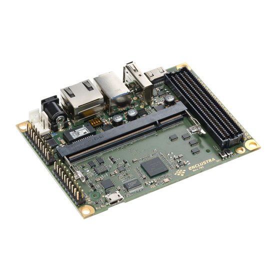
2.4 Top View Figure 3: Top view 23/04/2019 9 / 43 Version 1.09... -
Page 10: Bottom View
2.5 Bottom View Figure 4: Bottom view 23/04/2019 10 / 43 Version 1.09... -
Page 11: Dimensions
2.6 Dimensions J800 (FPGA JTAG), J801 (FX3 Connector) and J1101 (IO Connector) are 2.54 mm pin headers. Figure 5: Dimensions 23/04/2019 11 / 43 Version 1.09... -
Page 12: Dip Switches
2.7 DIP Switches The tables below show the functions of the configuration DIP switches. The options printed bold are the default settings. Switch (CFG-A / S1200) Reserved (will be VCC_IO = 1.8V in VCC_IO is 2.5V or 3.3V future versions) (depending on Switch 2) VCC_IO is 2.5V VCC_IO is 3.3V... -
Page 13: Connector Pinouts
2.8 Connector Pinouts Table 4 shows an overview of all connectors assembled on the Mars PM3 Board. A more detailed description of each connector can be found further below in this section. Connector Description Connected to J200 Mars Module Connector Mars FPGA module J400 USB 2.0 Micro-B Connector... - Page 14 VCC_5V PCIE_REFCLK_P VCC_5V PCIE_REFCLK_N PGOOD_CARRIER PCIE_PET1_P PCIE_PER1_P PCIE_PET1_N PCIE_PER1_N PCIE_PET0_P PCIE_PER0_P PCIE_PET0_N PCIE_PER0_N FMC_LA31_P FMC_LA33_P FMC_LA31_N FMC_LA33_N UART_TXD FMC_LA32_P UART_RXD FMC_LA32_N PWR_GOOD_MOD VMON_P41 VMON_P42 FMC_LA17_CC_P FMC_LA19_P FMC_LA17_CC_N FMC_LA19_N FMC_LA20_P FMC_LA18_CC_P FMC_LA20_N FMC_LA18_CC_N VCC_IO FMC_LA22_P FMC_LA21_P FMC_LA22_N FMC_LA21_N FMC_LA24_P FMC_LA23_P FMC_LA24_N FMC_LA23_N VCC_IO FMC_LA26_P...
- Page 15 FMC_LA16_P FMC_LA30_N FMC_LA16_N VCC_IO FMC_LA02_P FMC_LA00_CC_P FMC_LA02_N FMC_LA00_CC_N VCC_OUT FMC_LA03_P FX3_DQ28 FMC_LA04_P FMC_LA03_N FX3_DQ29 FMC_LA04_N VMON_P94 FMC_LA05_P FX3_DQ25 FX3_DQ24 FMC_LA06_P FMC_LA05_N FX3_DQ26 FX3_DQ27 FMC_LA06_N VCC_OUT FMC_LA07_P FX3_DQ31 FMC_LA01_CC_P FMC_LA07_N FX3_DQ30 FMC_LA01_CC_N VMON_P106 FMC_LA09_P FX3_DQ18 FX3_DQ21 FMC_LA08_P FMC_LA09_N FX3_DQ16 FX3_DQ22 FMC_LA08_N FMC_CLK0_M2C_P FX3_DQ19 FMC_LA10_P...
-
Page 16: J400 - Usb 2.0 Micro-B Connector
SD_D2 FX3_DQ3 FX3_DQ4 SD_D3 FX3_DQ1 FX3_DQ6 SD-Card detect UART_RX FX3_DQ0 FX3_DQ5 UART_TX FX3_DQ2 JTAG_TCK USB_DP JTAG_TDI USB_DM JTAG_TMS USB_VBUS JTAG_TDO USB_ID USB_CPEN RSVD_P168 ETH_A_N RSVD_P170 BOOT_MODE1 ETH_A_P ETH0_LED1# I2C_INT# ETH0_LED2# I2C_SDA ETH_B_N I2C_SCL ETH_B_P ETH_CTREF FLASH _CLK ETH_C_N FLASH_DO ETH_C_P FLASH_DI ETH1_LED1# FLASH_CS#... -
Page 17: J500 - Usb 3.0 B Connector
and 155 for use with SOC modules. Please note that these pins are shared with the FX3 FIFO interface and must only be used as UART if the FX3 FIFO interface is not used! Power and data signals on this connector are protected against ESD incidents. 2.8.3 J500 –... -
Page 18: J801 - Fx3 Connector
Comment Signal Connector Pin Signal Comment VCC_IO VCC_IO SRST#_RDY# FPGA_TDI FPGA_TMS FPGA_TCK FPGA_TDO Not Connected SVD_P168 SVD_P170 Table 6: J800 – FPGA JTAG connector 2.8.7 J801 – FX3 Connector The main purpose of this connector is to access the JTAG port of the Cypress FX3 USB 3.0 controller. In addition, this connector feeds out four GPIO pins of the FX3 that can be used if the slave FIFO interface is not operated in 32 Bit mode. -
Page 19: J1000 - Mini Hdmi Connector
Table 8: J1000 – mini HDMI connector 2.8.9 J1100 – FMC LPC Connector This connector allows extending Mars PM3 boards with Enclustra (e.g. FMC DR2 Module) or third-party 160 pin LPC FMC modules. Warning The IO pins are directly connected to the FPGA. Only apply VCC_IO compliant voltages to the IO pins. - Page 20 FMC_CLK0_M2C_P FMC_CLK0_M2C_N FMC_LA00_CC_P FMC_LA02_P FMC_LA00_CC_N FMC_LA02_N FMC_LA03_P FX3_DQ28 FMC_LA04_P FMC_LA03_N FX3_DQ29 FMC_LA04_N FMC_LA08_P FX3_DQ21 FMC_LA07_P FMC_LA08_N FX3_DQ22 FMC_LA07_N FMC_LA12_P FX3_DQ20 FMC_LA11_P FMC_LA12_N FX3_DQ17 FMC_LA11_N FMC_LA16_P FMC_LA15_P FMC_LA16_N FMC_LA15_N FMC_LA20_P FMC_LA19_P FMC_LA20_N FMC_LA19_N FMC_LA22_P FMC_LA21_P FMC_LA22_N FMC_LA21_N FMC_LA25_P FMC_LA24_P FMC_LA25_N FMC_LA24_N FMC_LA29_P FMC_LA28_P FMC_LA29_N...
-
Page 21: Table 9: J1100A - Fmc Lpc Connector
VCC_IO VCC_IO Table 9: J1100A – FMC LPC connector Comment Signal Connector Pin Signal Comment PGOOD_SYSTEM Not Connected Not Connected Not Connected Not Connected Not Connected Not Connected FX3_DQ31 FMC_LA01_CC_P FX3_DQ30 FMC_LA01_CC_N FMC_LA06_P FX3_DQ24 FX3_DQ25 FMC_LA05_P FMC_LA06_N FX3_DQ27 FX3_DQ26 FMC_LA05_N FX3_DQ18 FMC_LA09_P FMC_LA10_P... -
Page 22: Table 10: J1100B - Fmc Lpc Connector
Not Connected FMC_I2C_SDA VCC_3V3 10k to VCC_3V3 10k to GND 10k to GND 10k to VCC_3V3 VCC_12V VCC_3V3 VCC_12V VCC_3V3 VCC_3V3 VCC_3V3 Table 10: J1100B – FMC LPC connector 23/04/2019 22 / 43 Version 1.09... -
Page 23: J1101 - Extension Connector (Not Assembled)
2.8.10 J1101 – Extension Connector (Not Assembled) This connector can be assembled as an alternative to the LPC FMC Connector. Warning The IO pins are directly connected to the FPGA. Only apply VCC_IO compliant voltages to the IO pins. Any other voltages may damage the FPGA as well as other devices on the Mars PM3 Board or the installed Mars FPGA module. -
Page 24: J1300 - Power Connector
Since the SD-Card holder was added subsequently on bootable pins (MIO40..45) of the Mars ZX3, it shares the pins with the FX3 USB3 controller. Therefore SD-Card and USB3 can’t be used simultaneously. Connector Pin Signal Data 0 FX3_SLOE#_SDD0 Data 1 FX3_PKTEND#_SDD1 Data 2 FX3_DQ3_SDD2... -
Page 25: J1302 - Fan Connector
Table 14: J1301 – Internal power connector 2.8.14 J1302 – Fan Connector At this connector a 12V fan with sense signal can be installed. Connector Pin Signal VCC_12V SYSMON_TACHO (Sense signal to determine fan speed) Table 15: J1302 – Fan connector 2.8.15 J1303 –... -
Page 26: Flash Configuration Multiplexer
2.9.2 Flash Configuration Multiplexer The Cypress FX3 USB 3.0 controller has its own SPI flash, where it can load the application and / or VID and PID during startup. If no valid boot image is found, the FX3 is waiting to receive the application code over USB. -
Page 27: Fifo Mode Multiplexer
Figure 6: Flash configuration multiplexer The control signals SPI_SEL, SPI_JTAG_EN# and SPI_CONFIG_EN# are connected to the Cypress FX3 USB 3.0 controller. For details refer to section 2.9.9. 2.9.3 Fifo Mode Multiplexer The slave fifo interface between the FPGA module and the Cypress FX3 USB 3.0 controller can be operated either in 16 or 32 Bit mode. -
Page 28: Figure 7: Fifo Mode Multiplexer
Figure 7: FIFO mode multiplexer The control signal FX3_PMODE0 is connected to the Cypress FX3 USB 3.0 controller. For details refer to section 2.9.9. 23/04/2019 28 / 43 Version 1.09... -
Page 29: Leds
2.9.4 LEDs Description Power Good: Indicates that DC-DC converters are in regulation. (D1202) FPGA Ready: The RDY LED shows the configuration status of the FPGA. The LED is on when a valid bitstream is loaded and off if no bitstream has been loaded or the FPGA (D1201) configuration has failed. -
Page 30: Rtc Battery
Table 21 shows the connection of the I C expander’s GPIO pins. I/O Bit Signal Description I/O[0] PCIE_PERST# PCIe reset signal I/O[1] 10k Pull up EEPROM_WP signal (user EEPROM write-protect signal) I/O[2] FX3_SLCS# Slave fifo chip select I/O[3] FX3_A0 Slave fifo address bit 0 I/O[4] USB_CPEN USB 2.0 power enable (Host connector J501) -
Page 31: System Monitor
2.9.8 System Monitor An I C system monitor (U1100) at address 0x2F is available on the Mars PM3 I C bus to monitor the supply voltages (1V2, 3V3, VCC_IO, 5V and 12V), read the FAN RPM’s and control two user GPIOs. It can be accessed by the FPGA and the Cypress FX3 USB 3.0 controller. -
Page 32: Figure 8: Location Of R326
3.0 controller includes a 32 Bit ARM926 core operating at 200 MHz using a 19.2 MHz crystal oscillator. It can access the I C bus, SPI flash of the FPGA and exchange debug or control information with the USB 2.0 UART controller over UART. A JTAG interface is available on connector J801 to debug and download the application. -
Page 33: Table 26: Usb 3.0 Controller Type
For more details refer to the CYUSB3014 datasheet and documentation Type Manufacturer CYUSB3014 Cypress Table 26: USB 3.0 Controller Type Table 27 shows the connection of the FX3 USB3 controller. Please note that the SD-Card and the user button share pins with the FX3 FIFO interface. Please note that the POR#_LOAD# and the I2C_INT# signals have been moved compared to previous versions. - Page 34 FPGA_DONE VCC_IO FPGA done signal SRST#_RDY# IN / OUT VCC_IO FPGA soft reset / ready signal POR#_LOAD# VCC_3V3 Hard Reset (FPGA_PROG_N) FX3_SCK VCC_3V3 SPI clock FX3_SS# VCC_3V3 SPI slave select FX3_DIN VCC_3V3 SPI data in FX3_DOUT VCC_3V3 SPI data out RSVD_P170 IN / OUT VCC_3V3...
-
Page 35: Table 27: Cypress Fx3 Usb 3.0 Controller Pinout
FX3_DQ17 IN / OUT VCC_IO Slave fifo data 17 / FMC_LA12_N FX3_DQ18 IN / OUT VCC_IO Slave fifo data 18 / FMC_LA09_P FX3_DQ19 IN / OUT VCC_IO Slave fifo data 19 / FMC_LA10_P FX3_DQ20 IN / OUT VCC_IO Slave fifo data 20 / FMC_LA12_P FX3_DQ21 IN / OUT VCC_IO... -
Page 36: Usb 2.0 Uart Device
2.9.10 USB 2.0 UART Device The USB 2.0 UART device controller (U401) is connected to J400 (USB 2.0 Micro-B connector). It allows exchanging debug and control commands between the host computer and the FPGA module or FX3. By default U401 is connected to both, the Mars module connector (Pins 34 and 36) and the FX3 controller (FX3_DQ28..31). -
Page 37: Absolute Maximum Ratings
3 Technical Data 3.1 Absolute Maximum Ratings Symbol Rating Unit VCC_MAIN_IN Supply voltage relative to GND -0.5 to 13.7 VCC_IO I/O input voltage relative to GND See Mars module user manual Temperature Temperature range for wide range modules (W) -25 to +85 °C Temperature range for commercial modules (C) 0 to + 65... -
Page 38: Mechanical Data
3.3 Mechanical data Symbol Value Size 100.0 x 72.0 mm (Pico ITX) Component height top 16 mm Component height bottom 4.5 mm (Battery holder) Weight 60 g (without Mars module) Table 30: Mechanical data 23/04/2019 38 / 43 Version 1.09... -
Page 39: Ordering
4 Ordering and support 4.1 Ordering Please use Enclustra's online request/order form for ordering or requesting information: http://www.enclustra.com/en/orderenquire/ 4.2 Support Please follow the instructions on Enclustra's online support site: http://www.enclustra.com/en/support/ 23/04/2019 39 / 43 Version 1.09... -
Page 40: Differential Pairs Net Lengths
Appendix A Differential pairs net lengths If using differential pairs, a differential impedance of 100 Ohm should be met on the extension. Make sure that the two nets of a differential pair have the same length. An Excel table1 lists the length of the differential pairs on the Mars module connector. This allows the user to match the total length of the differential pairs on an extension board if required for the application. - Page 41 Figures Figure 1: Mars PM3 board overview ............................7 Figure 2: Module label ................................. 8 Figure 3: Top view ..................................9 Figure 4: Bottom view ................................10 Figure 5: Dimensions ................................. 11 Figure 6: Flash configuration multiplexer .......................... 27 Figure 7: FIFO mode multiplexer............................28 Figure 8: Location of R326 ...............................
- Page 42 Table 22: I C EEPROM Type ..............................30 Table 23: I C System Monitor Type ............................31 Table 24: I C System monitor pin assignment ......................... 31 Table 25: Boot mode settings ..............................32 Table 26: USB 3.0 Controller Type ............................33 Table 27: Cypress FX3 USB 3.0 controller pinout ......................
- Page 43 References Enclustra Download Page http://download.enclustra.com/#Mars_PM3 Enclustra General Business Conditions http://www.enclustra.com/en/products/gbc/ Semtech SX150x datasheet: www.semtech.com 24AA128 EEPROM datasheet: www.microchip.com LM96080 datasheet: www.national.com CYUSB3014 datasheet: www.cypress.com 23/04/2019 43 / 43 Version 1.09...
Need help?
Do you have a question about the Mars PM3-R5 and is the answer not in the manual?
Questions and answers