Table of Contents
Advertisement
Quick Links
Advertisement
Table of Contents

Subscribe to Our Youtube Channel
Related Manuals for Artesyn MVME7616E Series

Summary of Contents for Artesyn MVME7616E Series
- Page 1 MVME7616E Transition Module Installation and Use P/N: 6806800A43F May 2016...
- Page 2 Artesyn reserves the right to revise this document and to make changes from time to time in the content hereof without obligation of Artesyn to notify any person of such revision or changes.
-
Page 3: Table Of Contents
Contents Contents About this Manual ............... . 9 General Information . - Page 4 Contents Contents Contents Asynchronous/Synchronous serial Port connectors (J7/J8) ....... 43 Parallel I/O Port Connector (J4) .
- Page 5 List of Tables Table 1-1 SIM Part Numbers ............. . 15 Table 1-2 MVME761 Transition Module Connectors .
- Page 6 List of Tables MVME7616E Transition Module Installation and Use (6806800A43F)
- Page 7 List of Figures Figure 1-1 RTM Front Panel and Components Side ........14 Figure 1-2 Three Row P2 Adapter .
- Page 8 List of Figures MVME7616E Transition Module Installation and Use (6806800A43F)
-
Page 9: About This Manual
About this Manual Overview of Contents This manual is divided into the following chapters and appendices: Chapter 1, General Information, on page 13 Chapter 2, Hardware Preparation and Installation, on page 21 Chapter 3, Functional Description, on page 27 Chapter 4, Connector Pin Assignments, on page 41 MVME7616E Transition Module Installation and Use provides general information, hardware preparation, installation instructions and support information for the MVME7616E-001 and MVME7616E-011 Transition Modules. - Page 10 About this Manual About this Manual Abbreviations This document uses the following abbreviations: Abbreviation Description Cubic Feet per Minute Data Communications Equipment Deutsches Insitut für Normung eV Data Terminal Equipment Electro-Magnetic Interference Electro-Static Discharge Federal Communications Commission Ground Integrated Circuit IEEE Institute of Electrical and Electronics Engineers PCI Mezzanine Card...
- Page 11 About this Manual Conventions The following table describes the conventions used throughout this manual. Notation Description 0x00000000 Typical notation for hexadecimal numbers (digits are 0 through F), for example used for addresses and offsets 0b0000 Same for binary numbers (digits are 0 and 1) bold Used to emphasize a word Used for on-screen output and code related elements...
- Page 12 May 2016 Removed Declaration of Conformity. 6806800A43E February 2016 Added Declaration of Conformity in Chapter 1, General Information on page 21. 6806800A43D April 2015 Re-branded to Artesyn template. 6806800A43C July 2009 Updated Table 1-6 6806800A43B August 2008 Updated to Emerson style.
-
Page 13: General Information
Chapter 1 General Information Overview This manual provides general information, hardware preparation, installation instructions, and a functional description for the MVME761-001 and MVME761-011 Transition Modules. The MVME761-0x1Transition Module provides the interface between the MVME5100 or MVME5500 Single Board Computer VMEmodules and various peripheral devices. This module provides industry standard connectors to simplify customer cable requirements for the serial port, printer, and Ethernet signals. -
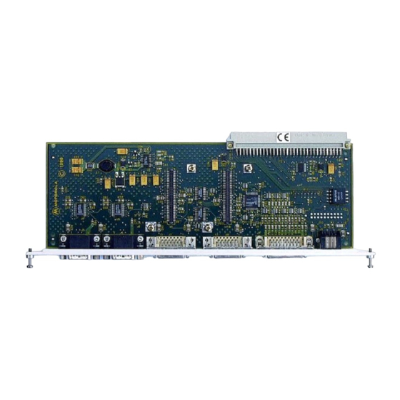
Page 14: Figure 1-1 Rtm Front Panel And Components Side
General Information Both MVME761-0x1 models use the same transition module. The MVME761-001 comes with a P2 adapter that connects to a 3-row DIN chassis backplane. The MVME761-011 comes with a P2 adapter that connects to a 5-row DIN chassis backplane. Figure 1-1 shows the MVME761 transition module component layout and the front panel. -
Page 15: Serial Port Interface Modules
EIA-232-D DTE SIM232DTE5E 01-W3877B11A Additional SIMs may be released. Please see your Artesyn representative for a complete list of SIMS that are available for the MVME761-0x1. P2 Adapter Boards The P2 adapters route the asynchronous and synchronous port, printer port, and Ethernet signals to the MVME761 transition module. -
Page 16: Three-Row P2 Adapter (Mvme761-001)
General Information Three-row P2 Adapter (MVME761-001) The P2 adapter for the MVME761-001 mounts onto a 3-row, 96-pin P2 backplane connector. The 50-pin male connector, J2, carries the 8-bit SCSI signals from the host VMEmodules. To run SCSI devices, you may install an additional transition module that is equipped with a SCSI port, such as the MVME712B. -
Page 17: Five-Row P2 Adapter (Mvme761-011)
General Information Five-Row P2 Adapter (MVME761-011) The P2 adapter for the MVME761-011 mounts onto a 5-row, 160-pin P2 backplane connector. The 68- pin female connector, J1, carries 16-bit SCSI signals from the host VMEmodules. It also has a 64-pin male connector, J3, for PMC I/O. Figure 1-3 Five Row P2 Adapter This P2 adapter, and the cable for connecting to the MVME761 transition module, can be... -
Page 18: Table 1-2 Mvme761 Transition Module Connectors
General Information 1. You will need to purchase or fabricate the port cables. Table 1-2 MVME761 Transition Module Connectors Type Number Description COM1 and 9-pin male DIN asynchronous serial port connector COM2 Serial port 3 26-pin female HD-26 synchronous serial port Serial port 4 connector Parallel port... -
Page 19: Specifications
General Information Table 1-5 Transition Module Cables Part Number Description Included with the 64-line flat ribbon cable with 96-pin DIN connectors that connects P2 MVME761-0x1 on the MVME761transition module to J3 on the 3-row P2 Adapter or J4 on the 5-row P2 adapter; 13 inches long. (30-W2799B02A). User-supplied EIA-232-D DTE or DCE cable (pins used depend on the processor VMEmodule) -
Page 20: 1.10 Cooling Requirements
General Information Table 1-6 MVME761-0x1 Specifications (continued) Characteristics Specifications Board Size Height: 9.187 inches(233.35 mm) (excluding front panel) Height: 3.200 inches(80.00 mm) Thickness: 0.063 inches (1.60 mm) MVME761P26E-001: 1.85" deep, 3.75" high MVME761026E-011: 2.725" deep, 3.75" high 1. J2 extends 1/4" further from the edge of the board. 1.10 Cooling Requirements The MVME761-0x1 is tested to operate under forced air cooling with an incoming air temperature range of 0 degrees C to 55 degrees C. -
Page 21: Hardware Preparation And Installation
Modules (SIMs). Unpacking the Hardware The MVME761 is packed in an antistatic wrapper to protect it from static discharge. Artesyn strongly recommends that you use an antistatic wrist strap and a conductive foam pad when handling the equipment. Electronic components can be extremely sensitive to electrostatic discharge (ESD). -
Page 22: Figure 2-2 Sim Configuration
Hardware Preparation and Installation You must set the jumpers and install the SIMs prior to installing the MVME761 transition module in the system chassis.The SIMs plug into connector J1 (for serial port 3) or J12 (for serial port 4) on the MVME761 transition module. Figure 2-2 SIM Configuration Mounting Hole... -
Page 23: Installing The Sim
Hardware Preparation and Installation Do not force the SIM onto the transition module. 4. Secure the SIM to the transition module standoffs with the two Phillips-head screws provided. Do not over tighten the screws. Figure 2-3 Installing the SIM 1911 9609 MVME7616E Transition Module Installation and Use (6806800A43F) -
Page 24: Installing The Transition Module And P2 Adapter
P2 connector on the transition module is not compatible with the P2 connector on the chassis backplane. Artesyn strongly recommends that you use an antistatic wrist strap and a conductive foam pad when installing or upgrading a system. Electronic components, such as disk drives, computer boards, and memory modules, can be extremely sensitive to electrostatic discharge (ESD). -
Page 25: Figure 2-4 Chassis Connections
Hardware Preparation and Installation Figure 2-4 Chassis Connections VME BACKPLANE MVME761 Transition Module Host Board 30-W2799B02A 64-CONDUCTOR P2 ADAPTER J3 ON THE 3-ROW P2 ADAPTER J4 ON THE 5-ROW P2 ADAPTER ENCLOSURE BOUNDARY 11654.00 9610 Procedure Follow these steps to configure, install, and cable the transition module. 1. - Page 26 Hardware Preparation and Installation 4. If necessary, move some of the other modules to allow space for the cables connected to the P2 adapter and the transition module. 5. Install the jumper on header J1 (on the 3-row P2 adapter or header J5 on the 5-row P2 adapter) if you are supporting SCSI devices.
-
Page 27: Functional Description
Chapter 3 Functional Description Overview This chapter provides information on MVME761 transition module and SIM circuitry, P2 signal multiplexing, and the configuration of the serial ports. Circuitry The MVME761 transition module and the Serial Interface Modules (SIMs) convert the TTL level signals to and from the MVME5100, and MVME5500 modules to the reception and transmission levels specified by the appropriate port interface standard. -
Page 28: Figure 3-1 Transition Module Block Diagram
Functional Description The block diagram for the MVME761 transition module is shown in Figure 3-1. The block diagram for the 3-row DIN backplane P2 adapter is shown in Figure 3-2. The block diagram for the 5-row DIN backplane P2 adapter is shown in Figure 3-3. -
Page 29: P2 Signal Multiplexing (P2Mx)
Functional Description Figure 3-2 3-Row DIN Backplane P2 Adapter Block Diagram 8-bit Single-ended SCSI 64-pin Connector to MVME761 Transition Module SCSI Terminators 3-Row Backplane Connector 11639.00 9611 Figure 3-3 5-Row DIN Backplane P2 Adapter Block Diagram 16-bit Single-ended SCSI 64-pin Connector to MVME761 Transition Module SCSI PMC I/O Terminators... - Page 30 Functional Description Four pins are used for the signal multiplexing: MXCLK MXSYNC# MXDO MXDI MVME7616E Transition Module Installation and Use (6806800A43F)
-
Page 31: Table 3-1 P2 Signal Multiplexing Sequence
Functional Description Sixteen time slots are defined and allocated. The signal multiplexing sequences are listed in the following table. Table 3-1 P2 signal multiplexing sequence MXDO (from the MVME510x/MVME550x) MXDI (from the MVME7616E) Time Slot Signal Name Time Slot Signal Name RTS3 CTS3 DTR3... -
Page 32: Serial Interface Module Circuitry
Functional Description MXSYNC# is clocked out using the falling edge of MXCLK and MDXO is clocked out with the rising edge of the MXCLK. MXDI is sampled at the rising edge of MXCLK (the transition module synchronizes MXDI with MXCLK’s rising edge). The timing relationships among MXCLK, MXSYNC#, MXDO, and MXDI are illustrated in the next figure. - Page 33 Functional Description EIA-232-D SIMs employ MC145406 ICs as line transmitters to convert the TTL output signals from the host VMEmodule to EIA-232-D voltage levels. As line receivers, the MC145406 ICs convert the EIA-232-D input signals to TTL voltage levels which are sent to the VME module. The MC145406 transceiver IC requires a series diode on the +12V supply and a clamp diode to logic ground on the -12V supply.
-
Page 34: Com1 And Com2 Asynchronous Serial Ports
Functional Description COM1 and COM2 Asynchronous Serial Ports The asynchronous serial port (COM1 and COM2) configuration is shown in the next figures. MVME7616E Transition Module Installation and Use (6806800A43F) -
Page 35: Figure 3-5 Eia-574 Dte Port Configuration
Functional Description Figure 3-5 EIA-574 DTE Port Configuration SOUT1 RTS1# DTR1# SIN1 COM1 CTS1# DSR1# DCD1# RI1# PC87308 P2/P2MX SOUT2 RTS2# DTR2# SIN2 COM2 CTS2# DSR2# DCD2# RI2# VME Module MVME761 Transition Module MVME7616E Transition Module Installation and Use (6806800A43F) -
Page 36: Asynchronous/Synchronous Serial Ports
Functional Description Asynchronous/Synchronous Serial Ports The asynchronous/synchronous serial port (Port 3 and Port 4) interface configuration diagrams are on the following pages. MVME7616E Transition Module Installation and Use (6806800A43F) -
Page 37: Figure 3-6 Eia232-Dce Configuration Port 3
Functional Description Figure 3-6 EIA232-DCE Configuration Port 3 MVME761 VME MODULE Z85230 SCC HD26 EIA232-DCE SIM RTS# CTS# DCD# TRXC RTXC P2/P2MX Z8536 CIO DTR# LLB# RLB# DSR# Header J18 1-2 Header J2 2-3 MVME7616E Transition Module Installation and Use (6806800A43F) -
Page 38: Figure
Functional Description Figure 3-7 EIA232-DCE Configuration Port 4 VME MODULE MVME761 Z85230 SCC HD26 EIA232-DCE SIM RTS# CTS# DCD# TRXC RTXC P2/P2MX Z8536 CIO DTR# LLB# RLB# DSR# Headers: J16 2-3 Header J3 2-3 J17 1-2 J19 1-2 MVME7616E Transition Module Installation and Use (6806800A43F) -
Page 39: Figure 3-8 Eia232-Dte Configuration Port 3
Functional Description Figure 3-8 EIA232-DTE Configuration Port 3 VME MODULE MVME761 Z85230 SCC HD26 EIA232-DTE SIM RTS# CTS# DCD# TRXC RTXC P2/P2MX Z8536 CIO DTR# LLB# RLB# DSR# Header J18 2-3 Header J2 1-2 MVME7616E Transition Module Installation and Use (6806800A43F) -
Page 40: Figure 3-9 Eia232-Dte Configuration Port 4
Functional Description Figure 3-9 EIA232-DTE Configuration Port 4 MVME761 VME MODULE Z85230 SCC HD26 EIA232-DTE SIM RTS# CTS# DCD# TRXC RTXC P2/P2MX Z8536 CIO DTR# LLB# RLB# DSR# Headers: J16 2-3 Header J3 1-2 J17 2-3 J19 1 2 MVME7616E Transition Module Installation and Use (6806800A43F) -
Page 41: Connector Pin Assignments
Chapter 4 Connector Pin Assignments Overview This chapter provides the pin assignments for the P2 connector and front panel port connectors on the MVME761 transition module, as well as for the SCSI and PMC I/O connectors on the P2 adapters. P2 Connector Signaling and power from the host VMEmodules are received through connector P2, a 64-pin DIN connector. - Page 42 Connector Pin Assignments Table 4-1 P2 Connector Pin Assignments (continued) Row A Pins Row C Pins Signal Signal AUTOFD# SELIN# TXD3 RXD3 RTXC3 TRXC3 TXD1_232 RXD1_232 RTS1_232 CTS1 TXD4 RXD4 RTXC4 TRXC4 No Connect -12VF MSYNC# MCLK TXD2_232 RXD2_232 RTS2_232 CTS2_232 MVME7616E Transition Module Installation and Use (6806800A43F)
-
Page 43: Asynchronous Serial Port Connectors (J5/J6)
Connector Pin Assignments Asynchronous Serial Port Connectors (J5/J6) The interface for the asynchronous serial ports, COM1 and COM2, is provided with two standard DB9 connectors, J5 and J6. The connector shields for these ports are tied to chassis ground. The pin assignments and signal mnemonics for these connectors are listed in Table 4-2. -
Page 44: Table 4-4 Serial Port 4 Pin Assignments
Connector Pin Assignments Table 4-3 Serial Port 3 Pin Assignments (continued) Signal Signal RXD3 SP3_P16 RTS3 RXCI3 CTS3 LLB3 DSR3 SP3_P19 DTR3 DCD3 RLB3 SP3_P9 SP3_P10 SP3_P23 SP3_P11 TXCO3 SP3_P12 SP3_P13 No Connect Table 4-4 Serial Port 4 Pin Assignments Signal Signal No Connect... -
Page 45: Parallel I/O Port Connector (J4)
Connector Pin Assignments Parallel I/O Port Connector (J4) The interface for the parallel port is a standard IEEE P1284-C, 36-pin connector, J4. The functionality of each signal depends on the mode of operation of this bidirectional Parallel Peripheral Interface. Refer to the IEEE P1284 D2.00 Standard for a complete description of each signal function. -
Page 46: Ethernet Connector (J9)
Connector Pin Assignments Ethernet Connector (J9) The 10Base-T/100Base-TX Ethernet interface is a RJ-45 connector, J9. The connector shield is tied to chassis ground. The pin assignments and signal mnemonics for this connector are listed Table 4-6. Table 4-6 10Base-T/100Base-TX Pin Assignments Signal Terminated Terminated... - Page 47 Connector Pin Assignments Table 4-7 8-bit SCSI Connector (3-Row P2 adapter) (continued) Signal Signal SDB1 SDB2 SDB3 SDB4 SDB5 SDB6 SDB7 No Connect MVME7616E Transition Module Installation and Use (6806800A43F)
-
Page 48: 3-Row P2 Adapter (J3)
Connector Pin Assignments 4.7.2 3-Row P2 Adapter (J3) The pin assignments and signal mnemonics for this connector are listed in Table 4-8. Table 4-8 VME Connector (3-Row P2 adapter) Signal Signal DCD3 DTR3 TXD1 RXD1 PRSTB_L RTS1 +12VF PRD0 CTS1 PRD2 PRD1 TXD4... -
Page 49: 5-Row P2 Adapter (J1)
Connector Pin Assignments Table 4-8 VME Connector (3-Row P2 adapter) (continued) Signal Signal PRFAULT_L TXD2 TXD3 RXD2 CTS2 RXD3 RTS2 CTS3 DCD2 RTS3 DTR2 4.7.3 5-Row P2 adapter (J1) The 16-bit SCSI connector on the 5-row DIN backplane P2 Adapter is a 68-pin connector, J1. The pin assignments and signal mnemonics for this connector are listed in Table 4-9. - Page 50 Connector Pin Assignments Table 4-9 16-bit SCSI Connector (5-Row P2 adapter) (continued) Signal Signal SDB7 DBP0 TERMPWR TERMPWR TERMPWR TERMPWR No Connect No Connect SDB8 SDB9 SDB10 SDB11 MVME7616E Transition Module Installation and Use (6806800A43F)
-
Page 51: Pmc I/O, 5-Row P2 Adapter (J3)
Connector Pin Assignments 4.7.4 PMC I/O, 5-Row P2 Adapter (J3) The PMC I/O connector on the 5-row DIN backplane P2 Adapter is a 64-pin connector, J3. The pin assignments and signal mnemonics for this connector are listed in Table 4-10. Table 4-10 PMC I/O Connector (5-Row P2 adapter) Signal Signal... -
Page 52: 5-Row P2 Adapter (J4)
Connector Pin Assignments Table 4-10 PMC I/O Connector (5-Row P2 adapter) (continued) Signal Signal PMCIO11 PMCIO27 PMCIO12 PMCIO28 PMCIO13 PMCIO29 PMCIO14 PMCIO30 PMCIO15 PMCIO31 4.7.5 5-Row P2 adapter (J4) The J4 connector on the 5-row P2 adapter is a VME, 64-pin male connector used for output to the P2 connector on the MVME761. - Page 53 Connector Pin Assignments Table 4-11 VME Connector (3-Row P2 adapter) (continued) Signal Signal PRD1 TXD4 PRD4 PRD3 RXD4 PRD6 PRD5 RTS4 PRD7 TRXC4 DTR4 PRACK_L CTS4 PRPE PRBSY DCD4 PRINIT_L PRSEL RTXC4 PRFAULT_L TXD2 TXD3 RXD2 CTS2 RXD3 RTS2 CTS3 DCD2 RTS3 DTR2...
- Page 54 Connector Pin Assignments MVME7616E Transition Module Installation and Use (6806800A43F)
- Page 56 Artesyn Embedded Technologies, Artesyn and the Artesyn Embedded Technologies logo are trademarks and service marks of Artesyn Embedded Technologies, Inc. All other product or service names are the property of their respective owners. © 2016 Artesyn Embedded Technologies, Inc.
Need help?
Do you have a question about the MVME7616E Series and is the answer not in the manual?
Questions and answers