
Subscribe to Our Youtube Channel
Related Manuals for YOKOGAWA DL1720E


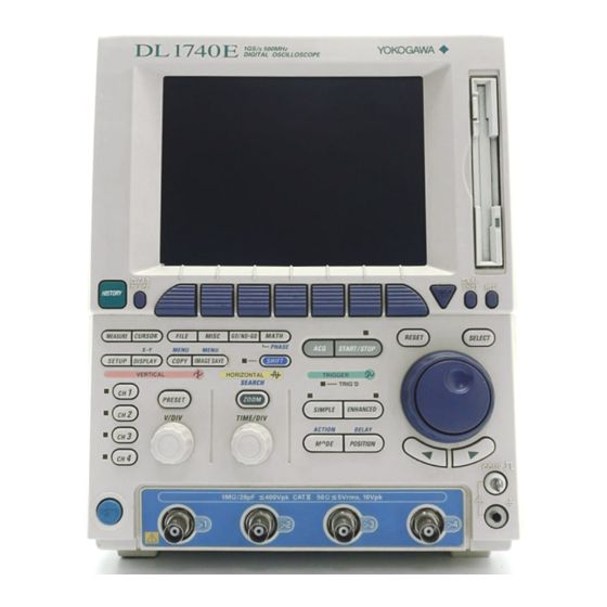
Summary of Contents for YOKOGAWA DL1720E
- Page 1 Service Manual DL1720E/DL1740E/DL1740EL Digital Oscilloscope SM 701730-01E 2nd Edition Yokogawa Electric Corporation...
- Page 2 YOKOGAWA instruments have been designed in a way that the replacement of electronic parts can be done on an assembly (module) basis by the user. YOKOGAWA instruments have also been designed in a way that troubleshooting and replacement of any faulty assembly can be done easily and quickly.
-
Page 3: Safety Precautions
To prevent an electric shock or fire, be sure to use the power cord supplied by YOKOGAWA. The main power plug must be plugged into an outlet with a protective grounding terminal. Do not disable protection by using an extension cord without protective grounding. - Page 4 Safety Precautions Safety Symbols Used on Equipment and in Manuals Improper handling or use can lead to injury to the user or damage to the instrument. This symbol appears on the instrument to indicate that the user must refer to the user’s manual for special instructions.
-
Page 5: Overview Of This Manual
Overview of This Manual This manual is meant to be used by qualified personel only. Make sure to read the safety precautions at the beginning of this manual and the warnings/cautions contained in any referenced chapter prior to carrying out any servicing. This manual contains the following chapters: 1 Principles of Operations Describes the functions of various assemblies and lists safety considerations. -
Page 6: Table Of Contents
Function of Each Assembly ..................1-2 Function of Each ASIC ..................... 1-6 Chapter 2 Performance Testing Introduction ......................2-1 Tests for the DL1720E/DL1740E/DL1740EL ............2-2 2.2.1 Grounding Test ..................... 2-3 2.2.2 Insulation Resistance Test ................2-4 2.2.3 Withstand Voltage ..................2-4 2.2.4 Selftest ......................2-4 2.2.5 GP-IB Test .................... - Page 7 Contents Chapter 7 Procedures for Disassembly Flow Chart of Disassembly ..................7-1 Removing the Top Cover ..................7-2 Removing the Fan Assy ................... 7-3 Removing the Printer Case ..................7-4 Removing the CPU Board Assy ................7-5 Removing the Printer Unit ..................7-6 Removing the Inverter Assy ..................
-
Page 8: Chapter 1 Principles Of Operation
The waveforms are displayed on the LCD using the data stored to the display memory. The block diagrams of the DL1720E are shown in figure 1.1 and figure 1.2. The block diagrams of the DL1740E/DL1740EL are shown in figure 1.3 and figure 1.4. Figure 1.1 and figure 1.3 are block diagrams of the circuit from the analog input to the A/D... - Page 9 The above-mentioned control signal, offset, and DC voltage for the trigger level are supplied by the analog front-end controller (AFC) IC on the AD4 board (or the AD2 board for the DL1720E) assembly. Table 1.1 Setting Range and Amplifying Level...
-
Page 10: Function Of Each Assembly
1.2 Function of Each Assembly AD4 Board (or AD2 Board for the DL1720E) Assembly The AD4 board (or AD2 board for the DL1720E) assembly has the time base, trigger, A/D converter, and analog control circuits onboard. The time base is of a PLL configuration. 1 GHz and 800 MHz can be switched. On the DL1720E/DL1740E/DL1740EL, the frequency of the clock is converted to 500 MHz or 400 MHz using high-speed ECL logic and distributed to each channel. - Page 11 Controls the exchange of signals between the CPU, KEY, ACQ4 (or the ACQ2 for the DL1720E), and a printer assembly. Supplies output from the power supply unit to the CPU, KEY, ACQ4 board (or the ACQ2 board for the DL1720E) assemblies, AD4 board (or the AD2 board for the DL1720E) assemblies, and a printer assembly.
- Page 12 1.2 Function of Each Assembly Ether Board Assembly (Optional) Option /C10 consists of an Ethernet interface section. The Ethernet interface section has an Ethernet controller. These interfaces are controlled by the CPU and CPU I/O interface (CIO) that are on the CPU board assembly. OPT TRIG Board Assembly (Optional) The OPT TRIG board assembly is equipped with a serial bus trigger logic (STL).
-
Page 13: Function Of Each Asic
1.3 Function of Each ASIC The following items describe the IC and the gate array function used in each assembly. Analog Front-End Controller (AFC) The AFC is a Bi-CMOS gate array. Its main functions are controlling the analog front- end circuit and assisting the trigger circuit. It includes a PWM signal output circuit used for D/A conversion, a parallel port, a serial port, a trigger hold-off circuit, an auto trigger circuit, a TV trigger generator, a fast counter, and a slow counter. - Page 14 1.3 Function of Each ASIC Figure 1.1 Block Diagram (Analog Section) of the DL1720E SM 701730-01E...
- Page 15 1.3 Function of Each ASIC Figure 1.2 Block Diagram (Digital Section) of the DL1720E SM 701730-01E...
- Page 16 1.3 Function of Each ASIC Figure 1.3 Block Diagram (Analog Section) of the DL1740E/DL1740EL SM 701730-01E...
- Page 17 1.3 Function of Each ASIC Figure 1.4 Block Diagram (Digital Section) of the DL1740E/DL1740EL 1-10 SM 701730-01E...
-
Page 18: Chapter 2 Performance Testing
Chapter 2 Performance Testing Introduction The aim of the tests in this chapter is to check the basic performance of the instrument. The order of the test procedures is just for convenience and does not need to be adhered to strictly. Please use the recommended equipment or their equivalents. Test Environment Operating Conditions •... -
Page 19: Tests For The Dl1720E/Dl1740E/Dl1740El
Tests for the DL1720E/DL1740E/DL1740EL Tests 2.2.1 Grounding Test 2.2.2 Insulation Resistance Test 2.2.3 Withstand Voltage 2.2.4 Selftest Memory Test Keyboard Test Printer Test (Only When the /B5 Option Is Installed) Floppy Disk Test (Only When the -J1 Option Is Installed) -
Page 20: Grounding Test
Confirm that a current of 30 A flows between the FG inlet of the AC power supply input and channel 4 of the BNC ground (or between FG and EXT. for the DL1720E), and that the resistance value is 0.1 Ω or less. -
Page 21: Insulation Resistance Test
2.2 Tests for the DL1720E/DL1740E/DL1740EL 2.2.2 Insulation Resistance Test Specifications: For DC 500 V, 10 MΩ or higher Testing Procedure Measure the insulation resistance between the AC power supply input signals below when the power switch is turned ON. DL1720E/DL1740E/... -
Page 22: Gp-Ib Test
2.2 Tests for the DL1720E/DL1740E/DL1740EL 2.2.5 GP-IB Test Test Items • APC with support for GP-IB • GP-IB cable Testing Procedure Connect the PC to the main unit with the GP-IB cable. Press MISC. The MISC menu appears. Press the Remote Control soft key. The Remote Cntl menu appears. -
Page 23: Rear Panel Probe Power Supply Test
Testing Procedure Connect the accessory probe (10:1) to the Probe Compensation terminal and input to an arbitrary channel. Execute Auto Setup. See section 4.5, “Executing Auto Setup” in the DL1720E/ DL1740E/DL1740EL user’s manual (IM 701730-01E) for the operating procedure. Probe Compensation Test Waveform... -
Page 24: Timebase Accuracy Test
DC–400 MHz (–3dB) DC 50 Ω (2 mV/div and 5 mV/div) DC–400 MHz (–3dB) 1 MΩ (probe terminal) Testing Procedure Execute calibration (see section 4.6, “Performing Calibration” in the DL1720E/ DL1740E/DL1740EL user’s manual (IM 701730-01E)). Enter the following settings on the DL1720E/DL1740E/DL1740EL. -
Page 25: Trigger Sensitivity Test
± (1% of the setting + 2 mV) 1 V/div–10 V/div: ± (1% of the setting + 20 mV) Testing Procedure Execute calibration (see section 4.6, “Performing Calibration” in the DL1720E/ DL1740E/DL1740EL user’s manual (IM 701730-01E)). Enter the following settings on the DL1720E/DL1740E/DL1740EL. CH (all channels) -
Page 26: Dc Accuracy
Apply a ±1 V offset to the channel under test, then confirm that the values obtained from automated measurement of waveform parameters (see section 10.6, “Automated Measurement of Waveform Parameters” in the DL1720E/ DL1740E/DL1740EL user’s manual (IM 701730-01E) lie within the judgment criteria on all channels. -
Page 27: Ext Trigger Level Accuracy Test
2.2 Tests for the DL1720E/DL1740E/DL1740EL 2.2.14 EXT Trigger Level Accuracy Test Specification: ± (10% of setting + 50 mV) Testing Procedure Enter the following settings on the DL1720E/DL1740E/DL1740EL. Display: V/div: 0.2 V/div Probe: Other than CH1 Display: DISPLAY Format: Single... -
Page 28: Ext Trigger Sensitivity And Trigger Out Test
2.2 Tests for the DL1720E/DL1740E/DL1740EL 2.2.15 EXT Trigger Sensitivity and Trigger Out Test Specification: Sensitivity 100 mV at 100 MHz Testing Procedure Enter the following settings on the DL1720E/DL1740E/DL1740EL. Display: V/div: 20 mV/div Probe: Coupling: DC 50 Ω Display: V/div:... -
Page 29: Ext Clock Input Test
2.2 Tests for the DL1720E/DL1740E/DL1740EL 2.2.16 EXT Clock Input Test Enter the following settings two channels at a time. Display: ON (other channels OFF) Enter the following settings on all channels, then perform steps 3, 4, and 5. CH (all channels) -
Page 30: Chapter 3 Adjustments
Do not drop the instrument, or allow it to fall over. • When feeding power with the DL1720E/DL1740E/DL1740EL cover open, apply a flow of air to the AD4 board (or the AD2 board for the DL1720E) and Power Supply (B8052YA*). -
Page 31: Test Environment
Test Environment Operating Conditions • Ambient temperature: 23 ±2˚C • Humidity: 55 ±10% RH • Voltage of power supply: Specified voltage ±1% • Frequency of power supply: Specified frequency ±1% Warm Up Time • More than thrity minutes after tuning ON the instrument. •... -
Page 32: Equipment Required
Equipment Required Table 3.1 Equipment Required Equipment Critical Specification Recommended Calibrator FLUKE (WAVETEK) 9500 Programmable Head Output Level: FLUKE (WAVETEK) 9520 Accuracy: < 0.02% Square Wave Frequency: 10 kHz Output Level: > 60 V Note The values shown in the specification column are those indicated by this service manual only. These values do not indicate the actual performances of the recommended equipment and tools. -
Page 33: Dc Offset Adjustment On The Ad Board
Press the SETUP key and select the Initialize soft key to execute initialization. Press the MISC key and select the Calibration soft key. Press the Cal Exec soft key to perform calibration. Enter the settings on the DL1720E/DL1740E/DL1740EL and calibrator as follows. DL1720E/DL1740E/DL1740EL VERTICAL (for all channels) - Page 34 3.4 DC Offset Adjustment on the AD Board R721 R707 R728 R714 Figure 3.2 Adjustment Point Location Diagram SM 701730-01E...
- Page 35 3.4 DC Offset Adjustment on the AD Board Figure 3.3 Observed Waveform SM 701730-01E...
-
Page 36: Flatness Adjustment On The Analog Board
Press the SETUP key and select the Initialize soft key to execute initialization. Press the MISC key and select the Calibration soft key. Select the Cal Exec soft key to perform calibration. For adjustment of the /10 range, enter the settings on the DL1720E/DL1740E/ DL1740EL oscilloscope and calibrator as follows. DL1720E/DL1740E/DL1740EL... - Page 37 3.5 Flatness Adjustment on the Analog Board For adjustment of the /100 range, enter the settings on the DL1720E/DL1740E/ DL1740EL oscilloscope and calibrator as follows. DL1720E/DL1740E/DL1740EL VERTICAL (for all channels) V/div: 1 V/div Position: 0 div Probe: HORIZONTAL T/div: 10 µs/div...
- Page 38 3.5 Flatness Adjustment on the Analog Board CV203 (CH2, CH4) CV103 (CH1, CH3) CV102 (CH1, CH3) CV202 (CH2, CH4) CV101 (CH1, CH3) CV201 (CH2, CH4) Figure 3.5 Adjustment Point Location Diagram Figure 3.6 Observed Waveform SM 701730-01E...
-
Page 39: Chapter 4 Troubleshooting
Chapter 4 Troubleshooting Introduction This chapter describes possible solutions for rectifying errors. In such cases, assembly removal may be required. Please heed the following warning. WARNING Assembly replacement is to be performed only by qualified service technicians who have experience working with the hazards involved (such as fire and electrical shock). -
Page 40: Flow Chart
DL1720E/DL1740E/DL1740EL while pressing the test results. RESET key. ‡ The monitor to be connected must be VGA supported. Maintenance Service is Required Contact your nearest YOKOGAWA representative as listed on the back cover of this manual. Figure 4.1 Troubleshooting Flow Chart SM 701730-01E... -
Page 41: Assemblies To Check When An Error Occurs
Assemblies to Check When an Error Occurs A short may occur in an assembly other than the power supply unit. To check in which voltage line a short has occurred, investigate each assembly to which voltage is supplied using a circuit tester. Table 4.1 “Correspondence of Assembly to Voltage” shows the relationship between assemblies and voltages supplied to them. - Page 42 Backup battery is flat. B8052MC CPU Board Assembly * Power Supply of the DL1720E/DL1740E/DL1740EL shipped before May 2005 is B9989YA, and Power Supply of the DL1720E/DL1740E/DL1740EL shipped since May 2005 is B8052YA. When trouble occurs, check the test item displaying FAIL and select the relevant defective item from table 4.3, “Correspondence of Test Items to Defective Assemblies.”...
- Page 43 4.3 Assemblies to Check When an Error Occurs When trouble occurs, check the non-conforming test and select the relevant defective assembly from table 4.4, “Correspondence of Test Items to Defective Assemblies.” If necessary, replace the relevant assembly. Table 4.4 Correspondence of Test Item to Defective Assemblies Test Item Assembly No.
-
Page 44: Power Supply Secondary Voltage
Power Supply Secondary Voltage Check whether the power supply secondary voltage fits the values listed on figure 4.2, “Power Supply Secondary Terminals” and Table 4.5, “Power Supply Secondary Terminal’s Name.” Figuer 4.2 Power Supply Secondary Terminals Table 4.5 Power Supply Secondary Terminal’s Name Pin No. -
Page 45: Chapter 5 Schematic Diagram
Chapter 5 Schematic Diagram Schematic Diagram Figure 5.1 Schematic Diagram of the DL1720E/DL1740E/DL1740EL SM 701730-01E... -
Page 46: Chapter 6 Customer Maintenance Parts List
Chapter 6 Customer Maintenance Parts List Customer Maintenance Parts List Ω Ω s , 1 Note: Parts marked with a symbol are Customer Maintenance Parts (CMP) . SM 701730-01E... - Page 47 6.1 Customer Maintenance Parts List Complete Set Ω / 2 0 < Ω < s , 1 Item Part No. Description Item Part No. Description B9989EC Support B9989DR Printer Case B9989DA Top Cover B9989CJ Frame Y9408LB B.H. Screw, M4x8 Main Assembly Y9408LB B.H.
- Page 48 6.1 Customer Maintenance Parts List Main Assembly 16 17 SM 701730-01E...
- Page 49 6.1 Customer Maintenance Parts List Item Part No. Description B9989DY Knob B9989DX Knob B8052DE Sheet (701715) (select) B8052DF Sheet (701730, 701740) B9989DK Knob B9989EL Spring B9989DL Knob B9969DK Lens B9989DM Knob B9969DE Knob B8052DA Front Bezel (701715) B8052DB Front Bezel (701730) (select) B8052DC Front Bezel (701740)
-
Page 50: Standard Accessories
Standard Accessories Standard Accessories Item Part No. Description A1006WD Power Supply Code (Suffix code-D, UL.CSA standard) A1253JZ 3P-2P Adapter A1006WD Power Supply Code (Suffix code-D, UL.CSA standard) A1009WD Power Supply Code (Suffix code-F, VDE standard) (select) A1054WD Power Supply Code (Suffix code-Q, BS standard) A1024WD Power Supply Code (Suffix code-R, AS standard) A1064WD... -
Page 51: Chapter 7 Procedures For Disassembly
Chapter 7 Procedures for Disassembly Flow Chart of Disassembly Top Cover (Section 7.2) (Section 7.3) Fan Assy (Section 7.4) Printer Case (Section 7.5) CPU Board Assy (Section 7.17) Ether Board Assy (Section 7.6) Printer Unit (Section 7.7) Inverter Assy (Section 7.8) Front Bezel (Section 7.9) PC Card Drive/FDD Assy... -
Page 52: Removing The Top Cover
Removing the Top Cover Remove the two screws from the rear panel as shown. Remove the four screws from the bottom of the instrument as shown. The top cover fits into the back of the front bezel. Remove the top cover by slowly pulling it away from the front bezel in the direction of the arrow as shown in the figure below. -
Page 53: Removing The Fan Assy
Removing the Fan Assy Remove the top cover. See section 7.2, “Removing the Top Cover.” Remove the cables on the right side panel as you face the instrument as shown in the figure below. Remove the three screws from the rear panel as shown in the figure. DL with the Fan Assy Removed SM 701730-01E... -
Page 54: Removing The Printer Case
Removing the Printer Case Remove the top cover. See section 7.2, “Removing the Top Cover.” Remove the printer cover by raising it in the direction of the arrow as shown below, then forcing it back until it pops out. Remove the screw from the printer case located toward the rear of the instrument. Lift the printer case to remove it, allowing the handle to slide through the opening in the case. -
Page 55: Removing The Cpu Board Assy
Removing the CPU Board Assy Remove the printer case. See section 7.4, “Removing the Printer Case.” Remove the screw from the left side panel as shown in the figure. Remove the screw from the right side panel as shown, then remove the multiconductor(s) (there are two multiconductors with a PC card, and one with a floppy disk drive). -
Page 56: Removing The Printer Unit
Removing the Printer Unit Remove the printer case. See section 7.4, “Removing the Printer Case.” Remove the two screws from the left side panel as shown in the figure below. Next, remove the handle and bracket in the direction of the arrow. DL with the Handle and Bracket Removed Remove the screw as shown in the figure below, then remove the roll paper holder in the direction of the arrow. - Page 57 7.6 Removing the Printer Unit Remove the two screws as shown in the figure below, then remove the cover in the direction of the arrow. Remove the cable in the direction of the arrow shown in the figure below. Remove the screws from the left side panel as shown in the figure below. Remove the screw from the right side panel as shown in the figure below.
- Page 58 7.6 Removing the Printer Unit Remove the two screws as shown in the figure below, then lift up the I/O device in the direction of the white arrow. DL with the I/O Device Removed Disconnect the three cable connectors as shown in the figure below, then remove the cables.
-
Page 59: Removing The Inverter Assy
Removing the Inverter Assy Remove the printer unit. See section 7.6, “Removing the Printer Unit.” Remove the two screws as shown, disconnect the three cables, then remove the assy. DL with the Inverter Assy Removed SM 701730-01E... -
Page 60: Removing The Front Bezel
Removing the Front Bezel Remove the printer case. See section 7.4, “Removing the Printer Case.” Pull out the three knobs in the direction of the arrow shown in the figure below and remove them. Note When the TIME/DIV and V/DIV knobs are removed, the “rib” holding the knob to its shaft becomes worn down causing the knob to become loose. -
Page 61: Removing The Pc Card Drive/Fdd Assy
Removing the PC Card Drive/FDD Assy Remove the front bezel. See section 7.8, “Removing the Front Bezel.” Remove the multiconductor(s) (there are two multiconductors with a PC card drive, and one with a floppy disk drive), then remove the two screws as shown in the figure below. -
Page 62: Removing The Key Board Assy
7.10 Removing the Key Board Assy Remove the front bezel. See section 7.8, “Removing the Front Bezel.” Remove the five screws as shown in the figure below. Remove the multiconductor as shown in the figure. DL with the Key Board Assy Removed 7-12 SM 701730-01E... -
Page 63: Removing The Lcd
7.11 Removing the LCD Remove the printer unit and the front bezel. See section 7.6, “Removing the Printer Unit” and section 7.8, “Removing the Front Bezel.” Remove the two cables, then remove the multiconductor as shown in the figure below. Remove the four screws as shown in the figure below. -
Page 64: Removing The Power Supply Assy
7.12 Removing the Power Supply Assy Remove the fan assy and the front bezel. See section 7.3, “Removing the Fan Assy” and section 7.8, “Removing the Front Bezel.” Remove the two screws, then remove the bracket as shown in the figure below. Remove the three screws as shown in the figure below. - Page 65 7.12 Removing the Power Supply Assy DL with the Power Supply Assy Removed 7-15 SM 701730-01E...
-
Page 66: Removing The Input Assy
7.13 Removing the Input Assy Remove the fan assy and the front bezel. See section 7.3, “Removing the Fan Assy” and section 7.8, “Removing the Front Bezel.” Remove the two screws as shown in the figure below. Remove the five screws as shown in the figure below. Remove the two screws, then remove the bracket as shown in the figure below. - Page 67 7.13 Removing the Input Assy Remove the left shield plate as shown in the figure below. Remove the right shield plate as shown in the figure below. Remove the cable as shown in the figure below. Lift up the front end of the board assy as shown in figure below (left), then pull it out in the direction of the rear panel as shown in figure below (right).
- Page 68 7.13 Removing the Input Assy DL with the Input Assy Removed 7-18 SM 701730-01E...
-
Page 69: Removing The Ad Board Assy
7.14 Removing the AD Board Assy Remove the input assy. See section 7.13, “Removing the Input Assy.” Note The AD Board Assy is easier to remove if you first remove the ACQ Board Assy. See section 7.16, “Removing the ACQ Board Assy.” Remove the four screws as shown in the figure below, then remove the nuts as shown in the figure below. - Page 70 7.14 Removing the AD Board Assy DL with the AD Board Assy Removed 7-20 SM 701730-01E...
-
Page 71: Removing The Analog Assy/Et2 Assy
7.15 Removing the Analog Assy/ET2 Assy Remove the input assy. See section 7.13, “Removing the Input Assy.” Remove the two screws, then remove the cover as shown in the figure below. Remove the screw as shown in the figure below. Remove the nuts as shown in the figure below. -
Page 72: Removing The Acq Board Assy
7.16 Removing the ACQ Board Assy Remove the input assy. See section 7.13, “Removing the Input Assy.” Remove the screw as shown in the figure below. Remove the six screws as shown in the figure below. DL with the ACQ Board Assy Removed 7-22 SM 701730-01E... -
Page 73: Removing The Ether Board Assy
7.17 Removing the Ether Board Assy Remove the CPU board assy. See section 7.5, “Removing the CPU board Assy.” Remove the three screws as shown in the figure below. DL with the Ether Board Assy Removed 7-23 SM 701730-01E...
Need help?
Do you have a question about the DL1720E and is the answer not in the manual?
Questions and answers