
Related Manuals for Motorola DSP56F803


Summary of Contents for Motorola DSP56F803
- Page 1 Order this document by DSP56F803EVMUM/D Semiconductor Products Sector Rev. 3.0, 02/2001 DSP56F803 Evaluation Module Hardware User’s Manual © Motorola, Inc., 2001. All rights reserved.
-
Page 3: Table Of Contents
DSP56F803 ........ - Page 4 2.16 Quadrature Encoder/Hall-Effect Interface......2-17 2.17 Zero-Crossing Detection ......... . 2-17 2.18 CAN Interface .
- Page 5 DSP56F803 Processor ........
- Page 6 A-11 Back-EMF and Phase Current Sense Analog Input Selectors ..A-12 A-12 Parallel JTAG Host/Target Interface and JTAG Connector..A-13 A-13 Power Supplies 3.3V and 5.0V....... . A-14 A-14 Bypass Capacitors and Spare Gates .
- Page 7 List of Tables DSP56F803EVM Default Jumper Options......1-3 RS-232 Serial Connector Description......2-5 Operating Mode Selection .
- Page 8 DSP56F803EVM Hardware User’s Manual...
-
Page 9: Audience
DSP56F803EVM. • Appendix B, DSP56F803EVM Bill of Material - provides a list of the materials used on the DSP56F803EVM board. Suggested Reading More documentation on the DSP56F803 and the DSP56F803EVM kit may be found at the URL: http://www.mot.com/SPS/DSP/documentation/index.html Preface... -
Page 10: Notation Conventions
CAN communications protocols. Digital Signal Processor or Digital Signal Processing Evaluation Module GPIO General Purpose Input and Output Port on Motorola’s Family of DSPs Integrated Circuit JTAG Joint Test Action Group. A bus protocol/interface used for test and debug. -
Page 11: References
Shares package pins with other peripherals on the chip and can function as a GPIO. OnCE On-Chip Emulation, a debug bus and port created by Motorola to enable designers to create a low-cost hardware interface for a professional quality debug environment. - Page 12 DSP56F803EVM Hardware User’s Manual...
-
Page 13: Introduction
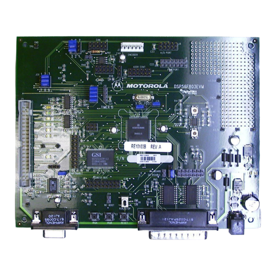
Chapter 1 Introduction The DSP56F803EVM is used to demonstrate the abilities of the DSP56F803 and to provide a hardware tool allowing the development of applications that use the DSP56F803. The DSP56F803EVM is an evaluation module board that includes a DSP56F803 part, peripheral expansion connectors, external memory, RS-232 interface and a CAN interface. -
Page 14: Block Diagram Of The Dsp56F803Evm
The DSP56F803EVM is flexible enough to allow a user to fully exploit the DSP56F803’s features to optimize the performance of their product, as shown in Figure 1-1. -
Page 15: Dsp56F803Evm Configuration Jumpers
DSP56F803EVM Configuration Jumpers 1.2 DSP56F803EVM Configuration Jumpers Ten jumper groups, (JG1-JG10), shown in Figure 1-2, are used to configure various features on the DSP56F803EVM board. Table 1-1 describes the default jumper group settings. JG10 7 8 9 JG10 DSP56F803EVM PWM LEDs JTAG USER LED RUN/STOP... -
Page 16: Dsp56F803Evm Connections
1.3 DSP56F803EVM Connections An interconnection diagram is shown in Figure 1-3 for connecting the PC and the external 12V DC power supply to the DSP56F803EVM board. Parallel Extension Cable DSP56F803EVM PC-compatible Computer Connect cable to Parallel/Printer port External with 2.1mm, receptacle Power connector... -
Page 17: Technical Summary
JTAG interface, makes the DSP56F803EVM ideal for developing and implementing many motor controlling algorithms, as well as for learning the architecture and instruction set of the DSP56F803 processor. The main features of the DSP56F803EVM include: •... - Page 18 [J10] • Connector to allow the user to connect to the DSP’s A/D Port [J9] • DSP56F803’s external memory expansion connectors [J7, J8 and J11] • On-board power regulation from an external 12V DC-supplied power input [P3] • Light Emitting Diode (LED) power indicator [LED1] •...
-
Page 19: Dsp56F803
DSP56F803 2.1 DSP56F803 The DSP56F803EVM uses a Motorola DSP56F803BU80 part, designated as U1 on the board and in the schematics. This part will operate at a maximum speed of 80MHz. A full description of the DSP56F803, including functionality and user information, is provided in the following documents: •... -
Page 20: Program And Data Memory
This memory bank will operate with zero wait-state accesses while the DSP56F803 is running at 70MHz. However, when running at 80MHz, the memory bank operates with four wait-state accesses. -
Page 21: Rs-232 Serial Communications
+3.3V signal levels to RS-232 compatible signal levels and connects to the host’s serial port via connector P4. Flow control is not provided, but could be implemented using uncommitted GPIO signals. The pinout of connector P4 is listed in Table 2-1. RS-232 Level Interface DSP56F803 RS-232 TXD0 T1in T1out RXD0 R1out R1in Figure 2-2. -
Page 22: Clock Source
The DSP56F803EVM provides a boot-up MODE selection jumper, JG4. This jumper is used to select the operating mode of the DSP as it exits RESET. Refer to the DSP56F803 User’s Manual for a complete description of the chip’s operating modes. -
Page 23: Debug Led
2.7.1 JTAG Connector The JTAG connector on the DSP56F803EVM allows the connection of an external Host Target Interface for downloading programs and working with the DSP56F803’s registers. This connector is used to communicate with an external Host Target Interface which passes information and data back and forth with a host processor running a debugger program. -
Page 24: Parallel Jtag Interface Connector
1–2 Disable on-board Parallel JTAG Interface 2.7.2 Parallel JTAG Interface Connector The Parallel JTAG Interface Connector, P2, allows the DSP56F803 to communicate with a Parallel Printer Port on a Windows PC; see Figure 2-5. By using this connector, the user can download programs and work with the DSP56F803’s registers. -
Page 25: Parallel Jtag Interface Connector Description
Debug Support Table 2-5. Parallel JTAG Interface Connector Description Pin # Signal Pin # Signal PORT_RESET PORT_IDENT PORT_TMS PORT_TCK PORT_TDI PORT_TRST PORT_IDENT PORT_VCC PORT_TDO PORT_CONNECT Table 2-6. On-Board Host Target Interface Power Source Jumper Selection Comment 1–2 Host supplied power 2–3 Target supplied power Technical Summary... -
Page 26: External Interrupts
Figure 2-6. Schematic Diagram of the User Interrupt Interface 2.9 Reset Logic is provided in the DSP56F803 to generate a clean power-on RESET signal. Additional, reset logic is provided to support the RESET signals from the JTAG connector, the Parallel JTAG Interface and the user RESET push-button; see Figure 2-7. -
Page 27: Power Supply
Figure 2-8. Power applied to the DSP56F803EVM is indicated with a Power-On LED, referenced as LED1. +12V DC +5.0V +5.0V DC +3.3V DC +3.3V DSP56F803 Regulator Regulator DSP56F803EVM PARTS Figure 2-8. Schematic Diagram of the Power Supply Technical Summary 2-11... -
Page 28: Uni-3 Connector Description
2.11 UNI-3 Interface Motor control signals from a family of motor driver boards can be connected to the EVM board via the UNI-3 connector/interface. The UNI-3 connector/interface contains all of the signals needed to drive and control the motor drive boards. These signals are connected to differing groups of the DSP’s input and output ports: A/D, TIMER and PWM. -
Page 29: Run/Stop Switch
A Run/Stop toggle switch is connected to GPIO signal AN7, as shown in Figure 2-9. An optional series resistor is provided which, when removed, allows the user to utilize the AN7 signal for other purposes. DSP56F803 +3.3V RUN/STOP SWITCH Figure 2-9. Run/Stop Switch Technical Summary... -
Page 30: Motor Control Pwm Signals And Leds
2.13 Motor Control PWM Signals and LEDs The DSP56F803 has a dedicated PWM unit. The unit contains six PWM, three Phase Current sense and four Fault input lines. The PWM lines are connected to the UNI-3 interface connector and to a set of six PWM LEDs via inverting buffers. The buffers are used to isolate and drive the DSP’s PWM outputs to the PWM LEDs. -
Page 31: Uni-3 Motor Protection Logic
Motor Protection Logic 2.14.1 UNI-3 Motor Protection Logic The UNI-3 DC Bus Over-Voltage signal is connected to the DSP’s PWM group’s fault input, FAULT0. The UNI-3 DC Bus Over-Current signal is connected to the DSP’s PWM group’s fault input, FAULT1. Additionally, the UNI-3 DC Bus Over-Voltage and Over-Current analog signals are connected to two DSP A/D inputs, AN0 and AN1, respectively. -
Page 32: Back-Emf And Motor Phase Current Sensing
2.15 Back-EMF and Motor Phase Current Sensing The UNI-3 connector supplies Back-EMF and Motor Phase Current signals from the three phases of a motor attached to a motor drive unit. The Back-EMF signals on the UNI-3 connectors are derived from a resistor divider network contained in the motor drive unit. These resistors divide down the attached motor’s Back-EMF voltages to a 0 to +3.3V level. -
Page 33: Quadrature Encoder/Hall-Effect Interface
Zero-Crossing signals or Quadrature Encoder/Hall-Effect signals. When in operation, the DSP will only monitor one set of signals, either the Encoder/Hall-Effect or the Zero-Crossing. Figure 2-13 shows the Zero-Crossing and Encoder/Hall circuits. ZERO_X_A DSP56F803 ZERO_X_B ZERO_X_C PHASEA FILTER +5.0V PHASEB... -
Page 34: Can Interface
2.18 CAN Interface The DSP56F803EVM board contains a CAN physical-layer interface chip that is attached to the MSCAN_RX and MSCAN_TX pins on the DSP56F803. The EVM board uses a Philips, PCA82C250, high speed, 1Mbps, physical layer interface chip. Due to the +5.0V operating voltage of the CAN chip, a pull-up to +5.0V is required to level shift the... -
Page 35: Peripheral Connectors
Peripheral Connectors 2.19 Peripheral Connectors The EVM board contains a group of Peripheral Expansion Connectors used to gain access to the resources of the DSP56F803. The following signal groups have Expansion Connectors: • External Memory Control • Encoder/Timer Channel • Timer Channel •... -
Page 36: Encoder/Timer Channel Expansion Connector
2.19.2 Encoder/Timer Channel Expansion Connector The Encoder/Timer Channel port is an MPIO port attached to the Timer expansion connector. The port can act as a Quadrature Decoder interface port or as a general purpose Timer port. Refer to Table 2-10 for the signals attached to the connector. -
Page 37: Address Bus Expansion Connector
Peripheral Connectors 2.19.4 Address Bus Expansion Connector The 16-bit Address bus connector contains the DSP’s external memory address signal lines. The upper 8 bits, A8 - A15, can also be used as Port A GPIO lines. See Table 2-12 for the Address bus connector information. Table 2-12. -
Page 38: Data Bus Expansion Connector
2.19.5 Data Bus Expansion Connector The 16-bit Data bus connector contains the DSP’s external memory data signal lines. Refer to Table 2-13 for the Data bus connector information. Table 2-13. External Memory Address Bus Connector Description Pin # Signal Pin # Signal +3.3V 2-22... -
Page 39: A/D Port Expansion Connector
Peripheral Connectors 2.19.6 A/D Port Expansion Connector The 8-channel Analog to Digital conversion port is attached to this connector. See Table 2-14 for connection information. Table 2-14. A/D Connector Description Pin # Signal GNDA +3.3VA 2.19.7 Serial Communications Port Expansion Connector The Serial Communications Port, SCI, is attached to this connector. -
Page 40: Serial Peripheral Interface Expansion Connector
2.19.8 Serial Peripheral Interface Expansion Connector The Serial Peripheral Interface, SPI, is attached to this connector. See Table 2-16 connection information. Table 2-16. SPI Connector Description Pin # Signal Pin # Signal SCLK MOSI MISO +3.3V 2.19.9 CAN Expansion Connector The CAN port is attached to this connector. -
Page 41: Pwm Port Expansion Connector
Test Points 2.19.10 PWM Port Expansion Connector The PWM port is attached to this connector. Refer to Table 2-18 for connection information. Table 2-18. PWM Port Connector Description Pin # Signal Pin # Signal ISA0 ISA1 ISA2 FAULT0 FAULT1 FAULT2 PWM0 PWM1 PWM2... - Page 42 2-26 DSP56F803EVM Hardware User’s Manual...
-
Page 43: Appendix Adsp56F803Evm Schematics
Appendix A DSP56F803EVM Schematics DSP56F803EVM Schematics... -
Page 44: Dsp56F803 Processor
D S P 5 6 8 0 3 EVM.DSN R e v. N u mber 1 . 3 Monday, June 22, 1998 Development Tools D a t e : D e s i g n er: S h e e t Figure A-1. DSP56F803 Processor... -
Page 45: Reset, Mode, Clock & Irqsl
+ 3 . 3 V R 1 6 1 0 K IRQA PUSHBUTTON OSC BYPASS J G 3 / I R Q A C 3 6 E X T AL 0 . 1 u F 1 0 M R 1 7 8 . -
Page 46: Program & Data Sram Memory
64Kx16-bit Program and 64Kx16-bit Data Memory / P S D [ 0 . . 1 5 ] A[0..15] D Q 1 D Q 2 D Q 3 D Q 4 D Q 5 D Q 6 D Q 7 D Q 8 D Q 9 D Q 1 0 D 1 0... -
Page 47: Rs-232 And Sci Connectors
C 4 0 0 . 1 u F + 3 . 3 V V C C C 4 1 C 4 2 C 2 + C 3 + C 4 3 0 . 1 u F 0 . 1 u F C 4 4 C 2 - C 3 -... -
Page 48: Dsp56F803 Pwm Leds And User Led
6 5 0 1 William Cannon Drive West Austin, TX, 78735-8598 (512)895-3230 FAX: (512)895-4556 MD:OE314 Title DSP56803 PWM LEDS AND USER LED Document Size DSP56803EVM.DSN Rev. N u m ber Date: Monday, June 22, 1998 Designer: Development Tools Sheet Figure A-5. DSP56F803 PWM LEDs and User LED... -
Page 49: Uni-3 Over-Voltage And Current Sense
UNI-3 OVER-VOLTAGE VOLTAGE SENSE FAULT DETECTION V_S_DCB +3.3V DSP PWM +5.0V 0.1uF FAULT SENSE 0 5.1K U14A +5.0V FAULT0 LM393A UNI-3 OVER-CURRENT CURRENT SENSE FAULT DETECTION I_S_DCB DSP PWM +3.3V +5.0V 0.1uF FAULT SENSE 1 5.1K U14B +5.0V FAULT1 LM393A Wireless Subscriber Division 6 5 0 1 William Cannon Drive West Austin, TX, 78735-8598... -
Page 50: Zero-Crossing/ Encoder Or Hall-Effect Selection
UNI-3: ZERO CROSSING Z E R O _ X _ A C O N N E C T Z E R O _ X _ B 1-2: ZERO CROSSING INFORMATION Z E R O _ X _ C 2-3: ENCODER / HALL EFFECT INFORMATION + 5 . -
Page 51: High Speed Can Interface
+ 5 . 0 V R 5 8 + 5 . 0 V DAISY-CHAIN CAN BUS CONNECTOR CAN BUS CONNECTOR U 1 5 M S C A N _ T X V C C M S C A N _ R X R X D V R E F T P 8 6... -
Page 52: Port Timer D, Address, Data, A/D And Control Line Connectors
PWM PORT ADDRESS BUS CONNECTOR 0-15 RAW CAN A[0..15] A[0..15] SIGNAL MSCAN_TX MSCAN_RX FAULT0 CONNECTOR FAULT1 FAULT2 PWM0 PWM1 PWM2 PWM3 PWM4 PWM5 +3.3V +3.3V PORT PA:0-7 SHARE ADDRESS BUS PINS A:8-15 CONTROL LINES DSP A/D PORT DATA BUS CONNECTOR 0-15 /IRQA D[0..15] D[0..15]... -
Page 53: Run/Stop Switch
TEST POINTS UNI-3 CONNECTOR +15VA UNI_3_+15 PWM_AT PWM0 PWM_AB PWM1 PWM_BT PWM2 PWM_BB PWM3 PWM_CT PWM4 PWM_CB PWM5 +5.0V_UNI3 +5.0V_UNI3 +3.3VA UNI_3_+15 UNI_3_-15 V_S_DCB I_S_DCB -15VA MOTOR PHASE A CURRENT SENSE U3_PHA_IS U3_PHB_IS MOTOR PHASE B CURRENT SENSE MOTOR PHASE C CURRENT SENSE U3_PHC_IS MOTOR DRIVE TEMPERATURE SENSE UNI_3_-15... -
Page 54: Back-Emf And Phase Current Sense Analog Input Selectors
J G 6 A B K _ E M F _ A A N 2 U 3 _ P H A _ I S J G 6 B B K _ E M F _ B A N 3 U 3 _ P H B _ I S J G 6 C B K _ E M F _ C A N 4... -
Page 55: Parallel Jtag Host/Target Interface And Jtag Connector
Parallel JTAG Interface PORT_IDENT P_RESET PORT_RESET PORT_TMS /TRST PORT_TCK TP46 TP47 PORT_TDI +3.3V +3.3V /PORT_TRST 5.1K 5.1K MC74HC244DW MC74HC244DW 5.1K 5.1K On-Board 5.1K PORT_VCC Host Target Interface Disable PORT_TDO 0.1uF PORT_CONNECT DB25M +3.3V On-Board Host Target Interface Power Source DSP /RESET JTAG Connector +3.3V DSP /JTAG-RESET... -
Page 56: Power Supplies 3.3V And 5.0V
FM4001 EXTERNAL POWER IN +5.0V_UNI3 +5.0V VOUT VOUT FM4001 470uF 0.1uF INPUT 12V DC 16VDC FERRITE BEAD MC33269DT_5.0 47uF 10VDC POWER GOOD LED LED1 GREEN LED +5.0V +3.3V +3.3VA FM4001 FERRITE BEAD 0.1uF VOUT VOUT +3.3V FERRITE BEAD FERRITE BEAD 47uF MC33269DT_3.3 10VDC... -
Page 57: Bypass Capacitors And Spare Gates
DSP56F803 UNI-3 UNI-3 CONTROL TIMER D GS72116 +5.0 VOLT +3.3 VA INTERFACE HEADER HEADER +3.3V +3.3VA +5.0V +3.3VA +3.3V +3.3V +5.0V +3.3V +3.3V 0.1uF 0.1uF 0.1uF 0.1uF 0.1uF 0.1uF 0.1uF 0.1uF 0.1uF 0.1uF 0.1uF 0.1uF 0.1uF ADDRESS BUS DATA BUS... - Page 58 A-16 DSP56F803EVM Hardware Reference Manual...
- Page 59 Appendix B DSP56F803EVM Bill of Material Description Ref. Designators Vendor Part # Integrated Circuits DSP56F803BU80 Motorola, DSP56F803BU80 GS72116TP-12 GSI, GS72116TP-12 ADM3311EARS Analog Devices, ADM3311EARS MC74HC244DW U6, U7 ON Semiconductor, MC74HC244DW MC33269DT-5.0 ON Semiconductor, MC33269DT-5.0 MC33269DT-3.3 ON Semiconductor, MC33269DT-3.3 74AC04SC U10, U12...
- Page 60 Description Ref. Designators Vendor Part # Resistors (continued) 24 Ω R47, R48, R50, R51, R53, SMEC RC73L2A24OHMJT R54, R56, R57 120 Ω, 1/4W YAGEO CFR 120QBK Potentioneters 10K Ω R40, R45 BC/MEPCOPAL ST4B103CT Inductors 1.0mH L1 - L4 Fair-Rite 2743015112 LEDs Green LED LED1, LED3, LED5, LED7,...
- Page 61 Description Ref. Designator Vendor Part # Jumpers 3 × 1 Bergstick JG3, JG8, J5, J12 SAMTEC TSW-103-07-S-S 4 × 2 Bergstick SAMTEC TSW-104-07-S-D 1 × 2 Bergstick JG2, JG4, JG5, JG9, JG10 SAMTEC TSW-102-07-S-S 3 x 3 Bergstick JG6, JG7 SAMTEC TSW-103-07-S-T 5 x 2 Bergstick J3, J9, J13...
- Page 62 DSP56F805EVM Hardware User’s Manual...
- Page 63 Index Numerics CAN interface CAN physical layer peripheral Clock Source 12VDC power supply Development Card DSP’s A/D Port external memory expansion connectors viii external oscillator frequency input GPIO compatible peripheral JTAG port interface MPIO compatible peripheral Back-EMF On-board power regulation signals 2-16 Operating Mode...
- Page 64 viii Quad Encoder 2-17 Quadrature Encoder/Hall-Effect 2-17 JTAG viii Connector connector Jumper Group RS-232 cable connection JG10 interface Schematic Diagram RS-232 Serial Communications Serial Communications Port 2-23 Serial Peripheral Interface 2-24 Jumper Options SRAM Jumper Settings external data external program Logic motor bus over-current Timer Channel...
- Page 66 Motorola product could create a situation where personal injury or death may occur.
Need help?
Do you have a question about the DSP56F803 and is the answer not in the manual?
Questions and answers