Table of Contents
Advertisement
Quick Links
Advertisement
Table of Contents

Subscribe to Our Youtube Channel
Related Manuals for SiFive FE310-G000


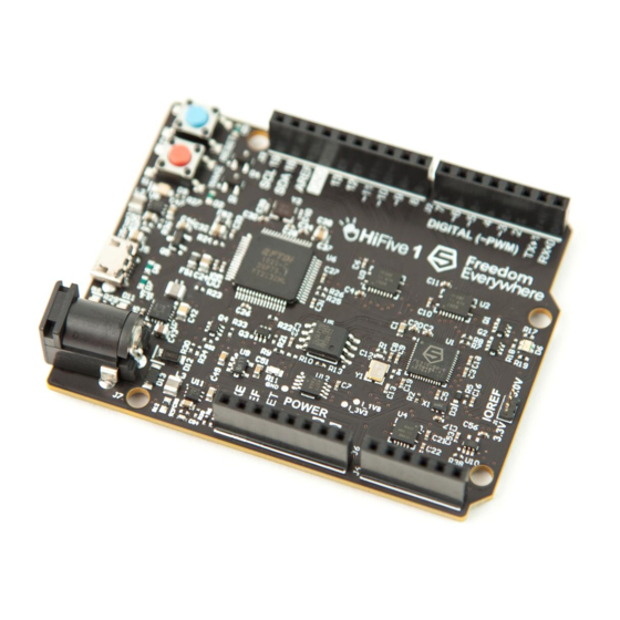
Summary of Contents for SiFive FE310-G000
- Page 1 SiFive FE310-G000 Manual v3p1 © SiFive, Inc.
- Page 2 SiFive does not assume any liability rising out of the application or use of any product or circuit, and specifically disclaims any and all liability, including without limitation indirect, incidental, spe- cial, exemplary, or consequential damages.
- Page 3 1.0.3 July 24, 2017 assignments 1.0.2 June 12, 2017 Clarify that QFN48 is the 6x6 Standard format • Add QFN48 Package Pinout 1.0.1 December 20, 2016 • Add Configuration String • Rename chip to FE310-G000 November 29, 2016 HiFive1 release...
-
Page 4: Table Of Contents
Contents Introduction ......................8 ....................8 FE310-G000 Overview ..................... 10 E31 RISC‑V Core ......................... 10 Interrupts ................... 11 On-Chip Memory System .................... 11 Always-On (AON) Block ......................11 GPIO Complex .............11 Universal Asynchronous Receiver/Transmitter ..............11 Hardware Serial Peripheral Interface (SPI) ..................... - Page 5 ..............21 5.1.4 Quad SPI Flash Controller (QSPI) ..................... 21 Reset and Trap Vectors Clock Generation ....................22 ..................22 Clock Generation Overview ..................23 PRCI Address Space Usage ........23 Internal Trimmable Programmable 72 MHz Oscillator (HFROSC) .............24 External 16 MHz Crystal Oscillator (HFXOSC) ................25 Internal High-Frequency PLL (HFPLL) ....................
- Page 6 ....................38 CLINT Memory Map ......................38 MSIP Registers ......................39 Timer Registers Platform-Level Interrupt Controller (PLIC) ...........40 ......................40 10.1 Memory Map ....................41 10.2 Interrupt Sources ....................42 10.3 Interrupt Priorities ....................42 10.4 Interrupt Pending Bits ..................... 43 10.5 Interrupt Enables ....................
- Page 7 15.2 RTC Configuration Register (rtccfg) ................67 15.3 RTC Compare Register (rtccmp) General Purpose Input/Output Controller (GPIO) ......69 ................. 71 16.1 GPIO Instance in FE310-G000 ......................71 16.2 Memory Map ....................71 16.3 Input / Output Values ........................ 72 16.4 Interrupts .....................
- Page 8 16.8 HW I/O Functions (IOF) Universal Asynchronous Receiver/Transmitter (UART) ....73 ...................... 73 17.1 UART Overview ................73 17.2 UART Instances in FE310-G000 ......................74 17.3 Memory Map ................74 17.4 Transmit Data Register (txdata) ................74 17.5 Receive Data Register (rxdata) .................75...
- Page 9 ....................... 88 19.1 PWM Overview ................89 19.2 PWM Instances in FE310-G000 ....................89 19.3 PWM Memory Map ................90 19.4 PWM Count Register (pwmcount) ..............91 19.5 PWM Configuration Register (pwmcfg) .................92 19.6 Scaled PWM Count Register (pwms) ............92 19.7 PWM Compare Registers (pwmcmp0–pwmcmp3) ..................
- Page 10 .................... 105 21.2 Resetting JTAG Logic ...................... 105 21.3 JTAG Clocking ................... 106 21.4 JTAG Standard Instructions ..................106 21.5 JTAG Debug Commands References ......................107...
-
Page 11: Introduction
Chapter 1 Introduction The FE310-G000 is the first Freedom E300 SoC, and forms the basis of the HiFive1 develop- ment board for the Freedom E300 family. The FE310-G000 is built around the E31 Core Com- plex instantiated in the Freedom E300 platform and fabricated in the TSMC CL018G 180nm process. - Page 12 Copyright © 2016–2019, SiFive Inc. All rights reserved. FE310G-0000 GPIO Complex 3.3V MOFF Pads UART0 UART1 1.8V MOFF Core E31 Core Complex PWM0 (8-bit) PWM1 (16-bit) GPIO Instruction Cache Ref ll M PWM2 (16-bit) Instruction Cache QSPI1 (16KiB, 2-way) QSPI2...
-
Page 13: E31 Risc-V Core
1.3 Interrupts The FE310-G000 includes a RISC-V standard platform-level interrupt controller (PLIC), which supports 51 global interrupts with 7 priority levels. The FE310-G000 also provides the standard RISC‑V machine-mode timer and software interrupts via the Core-Local Interruptor (CLINT). Interrupts are described in Chapter 8. The CLINT is described in Chapter 9. The PLIC is... -
Page 14: On-Chip Memory System
1.8 Hardware Serial Peripheral Interface (SPI) There are 3 serial peripheral interface (SPI) controllers. Each controller provides a means for serial communication between the FE310-G000 and off-chip devices, like quad-SPI Flash mem- ory. Each controller supports master-only operation over single-lane, dual-lane, and quad-lane protocols. -
Page 15: Pulse Width Modulation
The PWM peripherals are described in Chapter 19. 1.10 Debug Support The FE310-G000 provides external debugger support over an industry-standard JTAG port, including 2 hardware-programmable breakpoints per hart. Debug support is described in detail in Chapter 20, and the debug interface is described in... -
Page 16: List Of Abbreviations And Terms
Chapter 2 List of Abbreviations and Terms... - Page 17 JTAG Joint Test Action Group Loosely Integrated Memory. Used to describe memory space delivered in a SiFive Core Complex but not tightly integrated to a CPU core. Physical Memory Protection PLIC Platform-Level Interrupt Controller. The global interrupt controller in a RISC-V system.
-
Page 18: E31 Risc-V Core
Chapter 3 E31 RISC-V Core This chapter describes the 32-bit E31 RISC‑V processor core used in the FE310-G000. The E31 processor core comprises an instruction memory system, an instruction fetch unit, an exe- cution pipeline, a data memory system, and support for global, software, and timer interrupts. -
Page 19: Instruction Fetch Unit
Copyright © 2016–2019, SiFive Inc. All rights reserved. 3.2 Instruction Fetch Unit The E31 instruction fetch unit contains branch prediction hardware to improve performance of the processor core. The branch predictor comprises a 40-entry branch target buffer (BTB) which predicts the target of taken branches, a 128-entry branch history table (BHT), which predicts the direction of conditional branches, and a 2-entry return-address stack (RAS) which predicts the target of procedure returns. -
Page 20: Data Memory System
See The RISC‑V Instruction Set Manual, Volume I: User-Level ISA, Version 2.1 for more infor- mation on the instructions added by this extension. 3.6 Hardware Performance Monitor The FE310-G000 supports a basic hardware performance monitoring facility compliant with The RISC‑V Instruction Set Manual, Volume II: Privileged Architecture, Version 1.10. The mcycle CSR holds a count of the number of clock cycles the hart has executed since some arbitrary time in the past. -
Page 21: Memory Map
Chapter 4 Memory Map The memory map of the FE310-G000 is shown in Table 3. - Page 22 Off-Chip Non-Volatile Memory Reserved 0x4000_0000 0x7FFF_FFFF DTIM (16 KiB) 0x8000_0000 0x8000_3FFF RWXCA On-Chip Volatile Memory Reserved 0x8000_4000 0xFFFF_FFFF Table 3: FE310-G000 Memory Map. Memory Attributes: R - Read, W - Write, X - Execute, C - Cacheable, A - Atomics...
-
Page 23: Boot Process
RAM. The debug RAM code can be used to bootstrap download of further code. 5.1.2 Mask ROM (MROM) MROM is fixed at design time, and is located on the peripheral bus on FE310-G000, but instruc- tions fetched from MROM are cached by the core’s I-cache. The MROM contains an instruction at address... -
Page 24: One-Time Programmable (Otp) Memory
Off-chip SPI devices can vary in number of supported I/O bits (1, 2, or 4). SPI flash bits contain all 1s prior to programming. 5.2 Reset and Trap Vectors FE310-G000 fetches the first instruction out of reset from . The instruction stored there 0x1000... -
Page 25: Clock Generation
AON block (Chapter 12) or the PRCI block (Section 6.2). 6.1 Clock Generation Overview Figure 2: FE310-G000 clock generation scheme Figure 2 shows an overview of the FE310-G000 clock generation scheme. Most digital clocks on the chip are divided down from a central high-frequency clock produced from either hfclk the PLL or an on-chip trimmable oscillator. -
Page 26: Prci Address Space Usage
The AON block contains registers with similar func- tions, but only for the AON block units. Table 4 shows the memory map for the PRCI on the FE310-G000. Offset Name... -
Page 27: External 16 Mhz Crystal Oscillator (Hfxosc)
Copyright © 2016–2019, SiFive Inc. All rights reserved. hfrosccfg: Ring Oscillator Configuration and Status ( hfrosccfg Register Offset Bits Field Name Attr. Rst. Description [5:0] Ring Oscillator Divider Register hfroscdiv [15:6] Reserved [20:16] Ring Oscillator Trim Register hfrosctrim 0x10 [29:21]... -
Page 28: Internal High-Frequency Pll (Hfpll)
Copyright © 2016–2019, SiFive Inc. All rights reserved. When used to drive the PLL, the 16 MHz crystal oscillator output frequency must be divided by two in the first-stage divider of the PLL (i.e., ) to provide an 8 MHz reference clock to the VCO. - Page 29 Figure 3: Controlling the FE310-G000 PLL output frequency. field encodes the reference clock divide ratio as a 2-bit binary value, where the pllr[1:0] value is one less than the divide ratio (i.e., =4).
-
Page 30: Pll Output Divider
Copyright © 2016–2019, SiFive Inc. All rights reserved. (MHz) Legal multiplier frequency (MHz) refr pllf Table 8: Valid PLL multiply ratios. The multiplier setting in the table is given as the actual multiply ratio; the binary value stored in field should be... -
Page 31: Internal Programmable Low-Frequency Ring Oscillator (Lfrosc)
Copyright © 2016–2019, SiFive Inc. All rights reserved. plloutdiv: PLL Final Divide Configuration ( plloutdiv Register Offset Bits Field Name Attr. Rst. Description [5:0] PLL Final Divider Value plloutdiv [7:6] Reserved [13:8] PLL Final Divide By 1 plloutdivby1 [31:14] Reserved... -
Page 32: Alternate Low-Frequency Clock (Lfaltclk)
This mux selection can only be controlled by external pads, it is not psdlfaltclksel controllable by software. 6.9 Clock Summary Table 11 summarizes the major clocks on the FE310-G000 and their initial reset conditions. At power-on reset, the AON domain is clocked by either the LFROSC or , as... -
Page 33: Power Modes
Chapter 7 Power Modes This chapter describes the different power modes available on the FE310-G000. The FE310-G000 supports three power modes: Run, Wait, and Sleep. 7.1 Run Mode Run mode corresponds to regular execution where the processor is running. Power consump- tion can be adjusted by varying the clock frequency of the processor and peripheral bus, and by enabling or disabling individual peripheral blocks. - Page 34 HFROSC at the default setting, and must reconfigure clocks to run from an alternate clock source (HFXOSC or PLL) or at a different setting on the HFROSC. Because the FE310-G000 has no internal power regulator, the PMU’s control of the power sup- plies is through chip outputs, .
-
Page 35: Interrupts
Instruction Set Manual, Volume II: Privileged Architecture, Version 1.10. 8.1 Interrupt Concepts The FE310-G000 supports Machine Mode interrupts. It also has support for the following types of RISC‑V interrupts: local and global. Local interrupts are signaled directly to an individual hart with a dedicated interrupt value. This... -
Page 36: Interrupt Operation
Copyright © 2016–2019, SiFive Inc. All rights reserved. Figure 4: FE310-G000 Interrupt Architecture Block Diagram. 8.2 Interrupt Operation If the global interrupt-enable is clear, then no interrupts will be taken. If mstatus.MIE is set, then pending-enabled interrupts at a higher interrupt level will preempt cur- mstatus.MIE... -
Page 37: Interrupt Control Status Registers
A summary of the fields related to interrupts in mstatus the FE310-G000 is provided in Table 12. Note that this is not a complete description of mstatus as it contains fields unrelated to interrupts. For the full description of... -
Page 38: Machine Interrupt Enable (Mie)
See Table 13 for a description of the register. See Table 14 for a description of the mtvec field. See Table 18 for the FE310-G000 interrupt exception code values. mtvec.MODE Mode Direct When operating in direct mode all synchronous exceptions and asynchronous interrupts trap to address. -
Page 39: Machine Interrupt Pending (Mip)
Copyright © 2016–2019, SiFive Inc. All rights reserved. 8.3.4 Machine Interrupt Pending ( The machine interrupt pending ( ) register indicates which interrupts are currently pending. register is described in Table 16. Machine Interrupt Pending Register Bits Field Name Attr. -
Page 40: Interrupt Priorities
• Machine timer interrupts 8.5 Interrupt Latency Interrupt latency for the FE310-G000 is 4 cycles, as counted by the numbers of cycles it takes from signaling of the interrupt to the hart to the first instruction fetch of the handler. -
Page 41: Core-Local Interruptor (Clint)
Chapter 9 Core-Local Interruptor (CLINT) The CLINT block holds memory-mapped control and status registers associated with software and timer interrupts. The FE310-G000 CLINT complies with The RISC‑V Instruction Set Manual, Volume II: Privileged Architecture, Version 1.10. 9.1 CLINT Memory Map Table 19 shows the memory map for CLINT on SiFive FE310-G000. -
Page 42: Timer Registers
Copyright © 2016–2019, SiFive Inc. All rights reserved. 9.3 Timer Registers is a 64-bit read-write register that contains the number of cycles counted from the mtime rtcclk input described in Chapter 12. A timer interrupt is pending whenever is greater than or... -
Page 43: Platform-Level Interrupt Controller (Plic)
Architecture, Version 1.10 and supports 51 interrupt sources with 7 priority levels. 10.1 Memory Map The memory map for the FE310-G000 PLIC control registers is shown in Table 20. The PLIC memory map has been designed to only require naturally aligned 32-bit memory accesses. -
Page 44: Interrupt Sources
10.2 Interrupt Sources The FE310-G000 has 51 interrupt sources. These are driven by various on-chip devices as listed in Table 21. These signals are positive-level triggered. In the PLIC, as specified in The RISC‑V Instruction Set Manual, Volume II: Privileged Architec-... -
Page 45: Interrupt Priorities
10.3 Interrupt Priorities Each PLIC interrupt source can be assigned a priority by writing to its 32-bit memory-mapped register. The FE310-G000 supports 7 levels of priority. A priority value of 0 is priority reserved to mean "never interrupt" and effectively disables the interrupt. Priority 1 is the lowest active priority, and priority 7 is the highest. -
Page 46: Interrupt Enables
Copyright © 2016–2019, SiFive Inc. All rights reserved. PLIC Interrupt Pending Register 1 ( pending1 Base Address 0x0C00_1000 Bits Field Name Attr. Rst. Description Interrupt 0 Pend- Non-existent global interrupt 0 is hard- wired to zero Interrupt 1 Pend- Pending bit for global interrupt 1... -
Page 47: Priority Thresholds
WARL field, where the FE310-G000 supports a maximum threshold of 7. threshold The FE310-G000 masks all PLIC interrupts of a priority less than or equal to . For threshold example, a value of zero permits all interrupts with non-zero priority, whereas a threshold value of 7 masks all interrupts. -
Page 48: Interrupt Completion
Copyright © 2016–2019, SiFive Inc. All rights reserved. pending interrupt. A successful claim also atomically clears the corresponding pending bit on the interrupt source. A FE310-G000 hart can perform a claim at any time, even if the MEIP bit in its (Table 16) register is not set. - Page 49 Copyright © 2016–2019, SiFive Inc. All rights reserved. PLIC Claim/Complete Register ( claim Base Address 0x0C20_0004 [31:0] Interrupt Claim/ A read of zero indicates that no inter- Complete for Hart rupts are pending. A non-zero read 0 M-Mode contains the id of the highest pending interrupt.
-
Page 50: One-Time Programmable Memory (Otp) Peripheral
Chapter 11 One-Time Programmable Memory (OTP) Peripheral This chapter describes the operation of the One-Time Programmable Memory (OTP) Controller. Device configuration and power-supply control is principally under software control. The con- troller is reset to a state that allows memory-mapped reads, under the assumption that the con- troller’s clock rate is between 1 MHz and 37 MHz. - Page 51 Copyright © 2016–2019, SiFive Inc. All rights reserved. Offset Name Description Programmed-I/O lock register 0x00 otp_lock OTP device clock signals 0x04 otp_ck OTP device output-enable signal 0x08 otp_oe OTP device chip-select signal 0x0C otp_sel OTP device write-enable signal 0x10 otp_we...
-
Page 52: Programmed-I/O Sequencing
Copyright © 2016–2019, SiFive Inc. All rights reserved. 11.3 Programmed-I/O Sequencing The programmed-I/O interface exposes the OTP device’s and power-supply’s control signals directly to software. Software is responsible for respecting these signals' setup and hold times. The OTP device requires that data be programmed one bit at a time and that the result be re- read and retried according to a specific protocol. -
Page 53: Otp Programming Procedure
Copyright © 2016–2019, SiFive Inc. All rights reserved. • OTP Memory must be programmed only while the power supply voltages remain within specification. 11.6 OTP Programming Procedure 1. LOCK the otp: a. Write 0x1 to otp_lock b. Check that 0x1 is read back from otp_lock c. -
Page 54: Always-On (Aon) Domain
Chapter 12 Always-On (AON) Domain The FE310-G000 supports an always-on (AON) domain that includes real-time counter, a watchdog timer, backup registers, low frequency clocking, and reset and power-management circuitry for the rest of the system. Figure 5 shows an overview of the AON block. -
Page 55: Aon Power Source
12.3 AON Reset Unit An AON reset is the widest reset on the FE310-G000, and resets all state except for the JTAG debug interface. An AON reset can be triggered by an external active-low reset pin ( ), or expiration of the... -
Page 56: Reset Cause
The Real-Time Clock is described in detail in Chapter 15. 12.8 Backup Registers The backup registers provide a place to store critical data during sleep. The FE310-G000 has 16 32-bit backup registers. 12.9 Power-Management Unit (PMU) The power-management unit (PMU) sequences the system power supplies and reset signals when transitioning into and out of sleep mode. - Page 57 Copyright © 2016–2019, SiFive Inc. All rights reserved. Offset Name Description wdog Configuration 0x000 wdogcfg Counter Register 0x008 wdogcount Scaled value of Counter 0x010 wdogs Feed register 0x018 wdogfeed Key Register 0x01C wdogkey Comparator 0 0x020 wdogcmp0 rtc Configuration 0x040...
- Page 58 Copyright © 2016–2019, SiFive Inc. All rights reserved. Offset Name Description Sleep program instruction 5 0x134 pmusleepi5 Sleep program instruction 6 0x138 pmusleepi6 Sleep program instruction 7 0x13C pmusleepi7 PMU Interrupt Enables 0x140 pmuie PMU Wakeup Cause 0x144 pmucause Initiate PMU Sleep Sequence...
-
Page 59: Watchdog Timer (Wdt)
Chapter 13 Watchdog Timer (WDT) The watchdog timer (WDT) is used to cause a full power-on reset if either hardware or software errors cause the system to malfunction. The WDT can also be used as a programmable periodic interrupt source if the watchdog functionality is not required. The WDT is implemented as an upcounter in the Always-On domain that must be reset at regular intervals before the count reaches a preset threshold, else it will trigger a full power-on reset. -
Page 60: Watchdog Clock Selection
Copyright © 2016–2019, SiFive Inc. All rights reserved. The counter is incremented at a maximum rate determined by the watchdog clock selection. Each cycle, the counter can be conditionally incremented depending on the existence of certain conditions, including always incrementing or incrementing only when the processor is not asleep. -
Page 61: Watchdog Compare Register (Wdogcmp)
Copyright © 2016–2019, SiFive Inc. All rights reserved. dividing the clock rate by , so for an input clock of 32.768 kHz, the LSB of will incre- wdogs ment once per second. The value of is memory-mapped and can be read as a single 16-bit value over the AON wdogs TileLink bus. -
Page 62: Watchdog Feed Address (Wdogfeed)
Copyright © 2016–2019, SiFive Inc. All rights reserved. 13.6 Watchdog Feed Address ( wdogfeed After a successful key unlock, the watchdog can be fed using a write of the value 0xD09F00D address, which will reset the register to zero. The full watchdog feed... -
Page 63: Power-Management Unit (Pmu)
Chapter 14 Power-Management Unit (PMU) The FE310-G000 power-management unit (PMU) is implemented within the AON domain and sequences the system’s power supplies and reset signals during power-on reset and when tran- sitioning the "mostly off" (MOFF) block into and out of sleep mode. -
Page 64: Pmu Overview
Copyright © 2016–2019, SiFive Inc. All rights reserved. 14.1 PMU Overview pm ukey pm usl eep aonr st aonr st sleep PMU State wakeup Countdown 2 Machine done del ay pm upr ogr am pm ucause sleep µPC wakeup µPC... -
Page 65: Pmu Key Register (Pmukey)
Copyright © 2016–2019, SiFive Inc. All rights reserved. Offset Name Description Wakeup program instruction 0 0x100 pmuwakeupi0 Wakeup program instruction 1 0x104 pmuwakeupi1 Wakeup program instruction 2 0x108 pmuwakeupi2 Wakeup program instruction 3 0x10C pmuwakeupi3 Wakeup program instruction 4 0x110... -
Page 66: Initiate Sleep Sequence Register (Pmusleep)
Copyright © 2016–2019, SiFive Inc. All rights reserved. The PMU output signals are registered and only toggle on PMU instruction boundaries. The out- put registers are all asynchronously set to 1 by aonrst PMU Instruction Format ( pmu(sleep/wakeup)iX Register Offset... -
Page 67: Pmu Interrupt Enables (Pmuie) And Wakeup Cause (Pmucause)
Copyright © 2016–2019, SiFive Inc. All rights reserved. signal has a fixed deglitch circuit that requires the signal remain asserted dwakeup dwakeup for two AON clock edges before being accepted. The conditioning circuit also resynchronizes signal to the AON dwakeup lfclk 14.7 PMU Interrupt Enables (... - Page 68 Copyright © 2016–2019, SiFive Inc. All rights reserved. Index Meaning External reset Watchdog timer reset Table 41: Reset cause values...
-
Page 69: Real-Time Clock (Rtc)
Chapter 15 Real-Time Clock (RTC) The real-time clock (RTC) is located in the always-on domain, and is clocked by a selectable low-frequency clock source. For best accuracy, the RTC should be driven by an external 32.768 kHz watch crystal oscillator, but to reduce system cost, can be driven by a factory- trimmed on-chip oscillator. -
Page 70: Rtc Configuration Register (Rtccfg)
Copyright © 2016–2019, SiFive Inc. All rights reserved. rtccounthi: High bits of Counter ( rtccounthi Register Offset 0x4C Bits Field Name Attr. Rst. Description [31:0] High bits of Counter rtccounthi Table 42: rtccounthi: High bits of Counter rtccountlo: Low bits of Counter (... - Page 71 Copyright © 2016–2019, SiFive Inc. All rights reserved. rtccmp0: Comparator 0 ( rtccmp0 Register Offset 0x60 Bits Field Name Attr. Rst. Description [31:0] Comparator 0 rtccmp0 Table 45: rtccmp0: Comparator 0...
-
Page 72: General Purpose Input/Output Controller (Gpio)
This chapter describes the operation of the General Purpose Input/Output Controller (GPIO) on the FE310-G000. The GPIO controller is a peripheral device mapped in the internal memory map. It is responsible for low-level configuration of actual GPIO pads on the device (direction, pull up-enable, and drive value ), as well as selecting between various sources of the controls for these signals. - Page 73 Copyright © 2016–2019, SiFive Inc. All rights reserved. Figure 9: Structure of a single GPIO Pin with Control Registers. This structure is repeated for each pin.
-
Page 74: Gpio Instance In Fe310-G000
Copyright © 2016–2019, SiFive Inc. All rights reserved. 16.1 GPIO Instance in FE310-G000 FE310-G000 contains one GPIO instance. Its address and parameters are shown in Table 46. Instance Number Address ngpio 0x10012000 Table 46: GPIO Instance 16.2 Memory Map The memory map for the GPIO control registers is shown in Table 47. The GPIO memory map has been designed to require only naturally-aligned 32-bit memory accesses. -
Page 75: Interrupts
Copyright © 2016–2019, SiFive Inc. All rights reserved. 16.4 Interrupts A single interrupt bit can be generated for each GPIO bit. The interrupt can be driven by rising or falling edges, or by level values, and interrupts can be enabled for each GPIO bit individually. -
Page 76: Universal Asynchronous Receiver/Transmitter (Uart)
The UART peripheral does not support hardware flow control or other modem control signals, or synchronous serial data transfers. 17.2 UART Instances in FE310-G000 FE310-G000 contains two UART instances. Their addresses and parameters are shown in Table 48. Instance Num-... -
Page 77: Memory Map
Copyright © 2016–2019, SiFive Inc. All rights reserved. 17.3 Memory Map The memory map for the UART control registers is shown in Table 49. The UART memory map has been designed to require only naturally aligned 32-bit memory accesses. Offset... -
Page 78: Transmit Control Register (Txctrl)
Copyright © 2016–2019, SiFive Inc. All rights reserved. Receive Data Register ( rxdata Register Offset Bits Field Name Attr. Rst. Description [7:0] Received data data [30:8] Reserved Receive FIFO empty empty Table 51: Receive Data Register 17.6 Transmit Control Register (... -
Page 79: Interrupt Registers (Ip And Ie)
Copyright © 2016–2019, SiFive Inc. All rights reserved. Receive Control Register ( rxctrl Register Offset Bits Field Name Attr. Rst. Description Receive enable rxen [15:1] Reserved [18:16] Receive watermark level rxcnt [31:19] Reserved Table 53: Receive Control Register 17.8 Interrupt Registers (... - Page 80 Copyright © 2016–2019, SiFive Inc. All rights reserved. The input clock is the bus clock . The reset value of the register is set to , which tlclk div_init is tuned to provide a 115200 baud output out of reset given the expected frequency of tlclk Table 56 shows divisors for some common core clock rates and commonly used baud rates.
-
Page 81: Serial Peripheral Interface (Spi)
SPI flash device and instead return immediately. Hardware interlocks ensure that the current transfer completes before mode transitions and control register updates take effect. 18.2 SPI Instances in FE310-G000 FE310-G000 contains three SPI instances. Their addresses and parameters are shown in Table... -
Page 82: Memory Map
Copyright © 2016–2019, SiFive Inc. All rights reserved. Instance Flash Controller Address cs_width div_width QSPI 0 Control 0x10014000 QSPI 1 0x10024000 QSPI 2 0x10034000 Table 58: SPI Instances 18.3 Memory Map The memory map for the SPI control registers is shown in Table 59. The SPI memory map has... -
Page 83: Serial Clock Divisor Register (Sckdiv)
Copyright © 2016–2019, SiFive Inc. All rights reserved. Offset Name Description Serial clock divisor 0x00 sckdiv Serial clock mode 0x04 sckmode Reserved 0x08 Reserved 0x0C Chip select ID 0x10 csid Chip select default 0x14 csdef Chip select mode 0x18 csmode... -
Page 84: Serial Clock Mode Register (Sckmode)
Copyright © 2016–2019, SiFive Inc. All rights reserved. The input clock is the bus clock . The reset value of the field is tlclk Serial Clock Divisor Register ( sckdiv Register Offset Bits Field Name Attr. Rst. Description [11:0] Divisor for serial clock. -
Page 85: Chip Select Default Register (Csdef)
Copyright © 2016–2019, SiFive Inc. All rights reserved. Chip Select ID Register ( csid Register Offset 0x10 Bits Field Name Attr. Rst. Description [31:0] csid Chip select ID. bits wide. Table 64: Chip Select ID Register 18.7 Chip Select Default Register (... -
Page 86: Delay Control Registers (Delay0 And Delay1)
Copyright © 2016–2019, SiFive Inc. All rights reserved. 18.9 Delay Control Registers ( delay0 delay1 registers allow for the insertion of arbitrary delays specified in units of delay0 delay1 one SCK period. field specifies the delay between the assertion of CS and the first leading edge of cssck SCK. -
Page 87: Transmit Data Register (Txdata)
Copyright © 2016–2019, SiFive Inc. All rights reserved. For flash-enabled SPI controllers, the reset value is , corresponding to 0x0008_0008 proto single, = Tx, = MSB, and = 8. For non-flash-enabled SPI controllers, the reset endian value is , corresponding to... -
Page 88: Receive Data Register (Rxdata)
Copyright © 2016–2019, SiFive Inc. All rights reserved. flag indicates whether the transmit FIFO is ready to accept new entries; when set, full writes to are ignored. The field returns when read. txdata data Transmit Data Register ( txdata Register Offset... -
Page 89: Receive Watermark Register (Rxmark)
Copyright © 2016–2019, SiFive Inc. All rights reserved. 18.14 Receive Watermark Register ( rxmark register specifies the threshold at which the Rx FIFO watermark interrupt triggers. rxmark The reset value is Receive Watermark Register ( rxmark Register Offset 0x54 Bits Field Name Attr. -
Page 90: Spi Flash Interface Control Register (Fctrl)
Copyright © 2016–2019, SiFive Inc. All rights reserved. 18.16 SPI Flash Interface Control Register ( fctrl When the bit of the register is set, the controller enters direct memory-mapped SPI fctrl flash mode. Accesses to the direct-mapped memory region causes the controller to automati- cally sequence SPI flash reads in hardware. -
Page 91: Pulse Width Modulator (Pwm)
Chapter 19 Pulse Width Modulator (PWM) This chapter describes the operation of the Pulse-Width Modulation peripheral (PWM). 19.1 PWM Overview Figure 10 shows an overview of the PWM peripheral. The default configuration described here has four independent PWM comparators ( –... -
Page 92: Pwm Instances In Fe310-G000
Copyright © 2016–2019, SiFive Inc. All rights reserved. Figure 10: PWM Peripheral 19.2 PWM Instances in FE310-G000 FE310-G000 contains three PWM instances. Their addresses and parameters are shown in Table 82. Instance Number Address ncmp cmpwidth 0x10015000 0x10025000 0x10035000 Table 82: PWM Instances 19.3 PWM Memory Map... -
Page 93: Pwm Count Register (Pwmcount)
PWM 3 compare register 0x2C pwmcmp3 Table 83: SiFive PWM memory map, offsets relative to PWM peripheral base address 19.4 PWM Count Register ( pwmcount The PWM unit is based around a counter held in . The counter can be read or written pwmcount over the TileLink bus. -
Page 94: Pwm Configuration Register (Pwmcfg)
Copyright © 2016–2019, SiFive Inc. All rights reserved. 19.5 PWM Configuration Register ( pwmcfg PWM Configuration Register ( pwmcfg Register Offset Bits Field Name Attr. Rst. Description [3:0] PWM Counter scale pwmscale [7:4] Reserved PWM Sticky - disallow clearing bits... -
Page 95: Scaled Pwm Count Register (Pwms)
Copyright © 2016–2019, SiFive Inc. All rights reserved. The 4-bit field scales the PWM counter value before feeding it to the PWM compara- pwmscale tors. The value in is the bit position within the register of the start of a... -
Page 96: Deglitch And Sticky Circuitry
Copyright © 2016–2019, SiFive Inc. All rights reserved. PWM 2 Compare Register ( pwmcmp2 Register Offset 0x28 Bits Field Name Attr. Rst. Description [15:0] PWM 2 Compare Value pwmcmp2 [31:16] Reserved Table 89: PWM 2 Compare Register PWM 3 Compare Register (... -
Page 97: Generating Left- Or Right-Aligned Pwm Waveforms
Copyright © 2016–2019, SiFive Inc. All rights reserved. bit disallows the registers from clearing if they are already set and pwmsticky pwmcmp is used to ensure interrupts are seen from the bits. pwmcmp 19.9 Generating Left- or Right-Aligned PWM Waveforms Figure 11: Basic right-aligned PWM waveforms. -
Page 98: Generating Arbitrary Pwm Waveforms Using Ganging
Copyright © 2016–2019, SiFive Inc. All rights reserved. This technique provides symmetric PWM waveforms but only when the PWM cycle is at the largest supported size. At a 16 MHz bus clock rate with 16-bit precision, this limits the fastest PWM cycle to 244 Hz, or 62.5 kHz with 8-bit precision. -
Page 99: Generating One-Shot Waveforms
Copyright © 2016–2019, SiFive Inc. All rights reserved. 19.12 Generating One-Shot Waveforms The PWM peripheral can be used to generate precisely timed one-shot pulses by first initializing the other parts of then writing a 1 to the bit. The counter will run for one... -
Page 100: Debug
Chapter 20 Debug This chapter describes the operation of SiFive debug hardware, which follows The RISC‑V Debug Specification 0.11. Currently only interactive debug and hardware breakpoints are sup- ported. 20.1 Debug CSRs This section describes the per-hart trace and debug registers (TDRs), which are mapped into... -
Page 101: Trace And Debug Data Registers (Tdata1-3)
Copyright © 2016–2019, SiFive Inc. All rights reserved. Trace and Debug Select Register tselect Bits Field Name Attr. Description [31:0] index WARL Selection index of trace and debug registers Table 93: tselect field is a WARL field that does not hold indices of unimplemented TDRs. Even if index can hold a TDR index, it does not guarantee the TDR exists. -
Page 102: Debug Control And Status Register (Dcsr)
Debug ROM. The debugger may use it as described in The RISC‑V Debug Specifi- cation 0.11. 20.2 Breakpoints The FE310-G000 supports two hardware breakpoint registers per hart, which can be flexibly shared between debug mode and machine mode. When a breakpoint register is selected with... - Page 103 Copyright © 2016–2019, SiFive Inc. All rights reserved. Breakpoint Control Register ( mcontrol Register Offset Bits Field Attr. Rst. Description Name WARL Address match on LOAD WARL Address match on STORE WARL Address match on Instruction FETCH WARL Address match on User Mode...
-
Page 104: Breakpoint Match Address Register (Maddress)
Copyright © 2016–2019, SiFive Inc. All rights reserved. breakpoint register giving the address 1 byte above the breakpoint range, and using the chain bit to indicate both must match for the action to be taken. NAPOT ranges make use of low-order bits of the associated breakpoint address register to... -
Page 105: Sharing Breakpoints Between Debug And Machine Mode
Copyright © 2016–2019, SiFive Inc. All rights reserved. Debug-mode breakpoint traps jump to the debug trap vector without altering machine-mode reg- isters. Machine-mode breakpoint traps jump to the exception vector with "Breakpoint" set in the register and with holding the instruction or data address that caused the trap. -
Page 106: Debug Ram (0X400-0X43F)
20.3.2 Debug RAM ( – 0x400 0x43f SiFive systems provide at least the minimal required amount of Debug RAM, which is 28 bytes for an RV32 system and 64 bytes for an RV64 system. 20.3.3 Debug ROM ( – 0x800 0xFFF This ROM region holds the debug routines on SiFive systems. -
Page 107: Debug Interface
Chapter 21 Debug Interface The SiFive FE310-G000 includes the JTAG debug transport module (DTM) described in The RISC‑V Debug Specification 0.11. This enables a single external industry-standard 1149.1 JTAG interface to test and debug the system. The JTAG interface is directly connected to input pins. -
Page 108: Resetting Jtag Logic
Copyright © 2016–2019, SiFive Inc. All rights reserved. Figure 13: JTAG TAPC state machine. 21.2 Resetting JTAG Logic The JTAG logic must be asynchronously reset by asserting the power-on-reset signal. This dri- ves an internal signal. jtag_reset Asserting resets both the JTAG DTM and debug module test logic. Because parts... -
Page 109: Jtag Standard Instructions
The JTAG DTM implements the BYPASS and IDCODE instructions. On the FE310-G000, the IDCODE is set to 0x10E31913 21.5 JTAG Debug Commands The JTAG DEBUG instruction gives access to the SiFive debug module by connecting the debug scan register between jtag_TDI jtag_TDO... -
Page 110: References
Chapter 22 References Visit the SiFive forums for support and answers to frequently asked questions: https://forums.sifive.com [1] A. Waterman and K. Asanovic, Eds., The RISC-V Instruction Set Manual, Volume I: User- Level ISA, Version 2.2, May 2017. [Online]. Available: https://riscv.org/specifications/ [2] ——, The RISC-V Instruction Set Manual Volume II: Privileged Architecture Version 1.10,...
Need help?
Do you have a question about the FE310-G000 and is the answer not in the manual?
Questions and answers