Table of Contents
Advertisement
Quick Links
Advertisement
Table of Contents

Related Manuals for PLX Technology PCI 9054RDK-860

Summary of Contents for PLX Technology PCI 9054RDK-860
- Page 1 PCI 9054RDK-860 Hardware Reference Manual...
- Page 3 PCI 9054RDK-860 Hardware Reference Manual Version 2.3 July 2005 Website: http://www.plxtech.com Technical Support: http://www.plxtech.com/support/ Phone: 408 774-9060 800 759-3735 Fax: 408 774-2169...
- Page 4 © 2005 PLX Technology, Inc. All rights reserved. PLX Technology, Inc. retains the right to make changes to this product at any time, without notice. Products may have minor variations to this publication, known as errata. PLX assumes no liability whatsoever, including infringement of any patent or copyright, for sale and use of PLX products.
- Page 5 About This Manual This manual provides information about the PCI 9054RDK-860 Rapid Development Kit (RDK), from a hardware perspective. It contains descriptions of all major functional circuit blocks on the board. This manual also includes the complete schematic and bill of materials.
-
Page 7: Table Of Contents
4.18 J ..........4-13 UMPERS AND ONNECTORS UMMARY 4.18.1 Configuration Jumpers (Resistors).......... 4-13 4.18.2 Jumpers, Test Points, and Connectors ........4-14 4.19 S ..............4-14 PECIAL ONSIDERATIONS PCI 9054RDK-860 Hardware Reference Manual v2.3 © 2005 PLX Technology, Inc. All rights reserved. - Page 8 REFERENCES ....................8-1 BILL OF MATERIALS & SCHEMATICS ............. 9-1 LIST OF FIGURES 3-1. PCI 9054RDK-860 S ..........3-1 IGURE YSTEM RCHITECTURE 4-1. MPC860 P (POM2)..........4-8 IGURE ERIPHERALS ONNECTOR PCI 9054RDK-860 Hardware Reference Manual v2.3 © 2005 PLX Technology, Inc. All rights reserved.
- Page 9 9-3. BOM – M ........... 9-3 ABLE ANUALLY NSERTED OMPONENTS 9-4. BOM – M ............9-3 ABLE ISCELLANEOUS OMPONENTS 9-5. BOM – C ........9-3 ABLE OMPONENTS HOULD SSEMBLED PCI 9054RDK-860 Hardware Reference Manual v2.3 © 2005 PLX Technology, Inc. All rights reserved.
-
Page 11: General Information
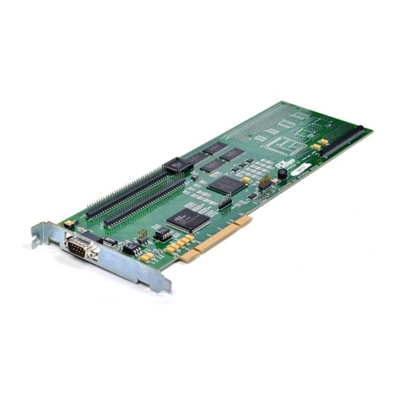
Through the use of this Rapid Development Kit, designs can be brought to market faster and more efficiently. Features The PCI 9054RDK-860 Rapid Development Kit contains a 12.35" L x 4.20" W circuit board, with the following features: •... -
Page 13: Hardware Installation
3. Ground yourself by touching the computer case. 4. Remove the computer cover. 5. Remove the PCI 9054RDK-860 circuit board from the antistatic bag and place it into an empty PCI slot. Secure the captive screw to ensure proper electrical grounding and mechanical stability. -
Page 15: System Architecture
MPC860 peripheral port connector MPC860 Serial Peripherals Port SDRAM FLASH MPC860 (32 MB) (512 KB) Local Bus PCI 9054 PCI Bus Figure 3-1. PCI 9054RDK-860 System Architecture PCI 9054RDK-860 Hardware Reference Manual v2.3 © 2005 PLX Technology, Inc. All rights reserved. - Page 16 Ready PCI 9054 architecture enables the PCI 9054RDK-860 to operate as an I O-compliant system. In addition, the PCI 9054RDK-860 provides the complete PCI SDK to aid programmers in developing drivers and applications. PCI 9054RDK-860 Hardware Reference Manual v2.3 © 2005 PLX Technology, Inc. All rights reserved.
-
Page 17: Hardware Architecture
2FFF FFFF Unused 2000 0000 1FFF FFFF Unused 1000 0000 01FF FFFF SDRAM space (32 MB) — controlled by SDRAM CS1# 5-1-1-1 0000 1000 MPC860 UPM(A) PCI 9054RDK-860 Hardware Reference Manual v2.3 © 2005 PLX Technology, Inc. All rights reserved. -
Page 18: Main Components
Motorola-approved tools including FRZ signal or VFLS[0:1] signal to pins 1 and 6. Refer to the Motorola website for further details on these tools. PCI 9054RDK-860 Hardware Reference Manual v2.3 © 2005 PLX Technology, Inc. All rights reserved. -
Page 19: Clock
The Local Bus Clock (CLKOUT) can be any multiple of 4 MHz, programmable with the MPC860 internal clock generator or 50 MHz with the 50 MHz external oscillator. The PCI 9054RDK-860 is built and set to 50 MHz with an external 50 MHz oscillator. -
Page 20: Memory
The length of the burst sequence may be set by the user and is programmed for one, two, four, eight, or whole page transfers within SDRAM Mode registers. PCI 9054RDK-860 Hardware Reference Manual v2.3 © 2005 PLX Technology, Inc. All rights reserved. - Page 21 Note: 100 MHz SDRAM were used to meet the MPC860 timing requirements. The SDRAM is accessible by way of the MPC860 or PCI 9054 (Host processor access). PCI 9054RDK-860 Hardware Reference Manual v2.3 © 2005 PLX Technology, Inc. All rights reserved.
- Page 22 ; Refresh (Offset 0x30) .long 0xeffebc04, 0x0ffc3c04, 0xfffffc04, 0xfffffc04 .long 0xfffffc04, 0xfffffc04, 0xfffffc04, 0xfffffc05 .long 0xfffffc04, 0xfffffc04, 0xfffffc04, 0xfffffc04 ; Exception (Offset 0x3c) .long 0xeffffc04, 0x0ffffc04, 0xfffffc05, 0xfffffc04 PCI 9054RDK-860 Hardware Reference Manual v2.3 © 2005 PLX Technology, Inc. All rights reserved.
-
Page 23: Serial Port
RS-232 port to monitor the PLX ROM program, which is stored in the FLASH. Debug Port The PCI 9054RDK-860 supports two MPC860 debug ports — JTAG(J2) and development port (BDM) (J3). The development port supports many different types of Motorola-approved tools, including the FRZ or VFLS[0:1] signals to pins 1 and 6. -
Page 24: Mpc860 Peripherals Connector (Pom2)
PB28 PB28 PB29 GPL_A2# 3,4,6,9,10 PB29 GPL_A2# PB30 GPL_A3# 3,4,6,9,10 PB30 GPL_A3# PB31 PB31 +12VCC +12VCC -12VCC -12VCC 3,6,10 PB[14:31] Figure 4-1. MPC860 Peripherals Connector (POM2) PCI 9054RDK-860 Hardware Reference Manual v2.3 © 2005 PLX Technology, Inc. All rights reserved. -
Page 25: Reset Circuitry
(MPC860 in this case) can reinitialize the PCI 9054, thereby overwriting the data from the serial EEPROM. Refer to PCI 9054 Data Book and the following serial EEPROM data example for more information. PCI 9054RDK-860 Hardware Reference Manual v2.3 © 2005 PLX Technology, Inc. All rights reserved. -
Page 26: Serial Eeprom Loads
MSW of PCI Configuration Address Register for 0000 DMCFGA[31:16] Direct Master-to-PCI I/O Configuration LSW of PCI Configuration Address Register for 0000 DMCFGA[15:0] Direct Master-to-PCI I/O Configuration 4-10 PCI 9054RDK-860 Hardware Reference Manual v2.3 © 2005 PLX Technology, Inc. All rights reserved. -
Page 27: Table 4-3. Extra Long Serial Eeprom Load Registers
LSW of Bus Region Descriptors (Space 1) for LBRD1[15:0] PCI-to-Local Accesses 0000 MSW of Hot Swap Control register Reserved 4C06 LSW of Hot Swap Control register HS_NEXT[7:0] / HS_CNTL[7:0] PCI 9054RDK-860 Hardware Reference Manual v2.3 4-11 © 2005 PLX Technology, Inc. All rights reserved. -
Page 28: Arbitration
4.15 Prototype Area The PCI 9054RDK-860 provides a prototype area that allows users to incorporate custom-designed circuitry. This area contains common surface-mount footprints, including two 44- pin TQFPs, two 20-pin SOs, two 16-pin SOs, a 20-pin PLCC, a 44-pin PLCC, and a 68-pin PLCC. -
Page 29: Jumpers And Connectors Summary
Power source. Refer to the section, ”Schematics, sheet 8.” Default. Install R51 and R54 for POM2 connector 3.3V/5VCC supply. R51/R52 and R53/R54—POM2 (Do not install R52 and R53.) Connect desired power supply combinations. PCI 9054RDK-860 Hardware Reference Manual v2.3 4-13 © 2005 PLX Technology, Inc. All rights reserved. -
Page 30: Jumpers, Test Points, And Connectors
Local Bus Control Signal test points. 4.19 Special Considerations Note the following when using the PCI 9054RDK-860: • BDIP# is generated only if the BTERM bit is reset (0). Therefore, if more than four Lwords are needed, use the BURST# signal (instead of BDIP#) to terminate the Burst sequence. -
Page 31: Software Architecture
Software Architecture PCI SDK A complete PCI 9054 API library is available from PLX Technology (refer to the section, “Customer Support,” for information on how to contact PLX). 5.1.1 PLXMon (Uses PCI SDK) PLXMon is used on the Host Bus (PC). PLXMon runs from FLASH memory on the Local Bus. -
Page 33: Serial Interface Pinout
PC[10] CD1# Carrier detect modem line for SCC1 Serial CAM Interface output signals that PB[14] RSTRT1# marks start of a frame PB[27] BRG01 BRG1 output clock PCI 9054RDK-860 Hardware Reference Manual v2.3 © 2005 PLX Technology, Inc. All rights reserved. -
Page 34: Table 6-4. Ethernet Controller
U18, R17, N16, P18, N17, N19, L16, K16, L19, K17, PB[14:31] PB[14:31] General Purpose I/O Port B bits [14:31] J18, J16, F19, E19, D19, E16, C19, C17 PCI 9054RDK-860 Hardware Reference Manual v2.3 © 2005 PLX Technology, Inc. All rights reserved. -
Page 35: Scc2
Clear to send modem line for SCC2 PC[9] CTS2# Carrier detect modem line for SCC2 PC[8] CD2# PA[6] CLK2 Input clock for SCC PB[26] BRG02 BRG2 output clock Note: No RSTRT# support. PCI 9054RDK-860 Hardware Reference Manual v2.3 © 2005 PLX Technology, Inc. All rights reserved. -
Page 36: Scc3
Clear to send modem line for SCC3 PC[6] CD3# Carrier detect modem line for SCC3 Clock for SCC PC[8] CLK3 Output clock for BRG3 PB[15] BRGOUT3 PCI 9054RDK-860 Hardware Reference Manual v2.3 © 2005 PLX Technology, Inc. All rights reserved. -
Page 37: Scc4
Request to send modem line for SCC4 PC[5] CTS4# Clear to send modem line for SCC4 PC[4] CD4# Carrier detect modem line for SCC4 BRG4 output clock PB[28] BRGO4 PCI 9054RDK-860 Hardware Reference Manual v2.3 © 2005 PLX Technology, Inc. All rights reserved. -
Page 38: Misc
Input transmit data sync to TDM Channel A PD[15] L1TSYNCA Receive sync input for serial interface PD[12] L1RSYNCB TDM Port B PD[13] L1TSYNCB Input transmit data sync to TDM Channel B PCI 9054RDK-860 Hardware Reference Manual v2.3 © 2005 PLX Technology, Inc. All rights reserved. -
Page 39: Customer Support
Address PLX Technology, Inc. Attn: Customer Support 870 Maude Ave Sunnyvale, CA 94085 Phone 408-774-9060 800-759-3735 408-774-2169 Website http://www.plxtech.com For technical support on the Web, go to http://www.plxtech.com/support/. PCI 9054RDK-860 Hardware Reference Manual v2.3 © 2005 PLX Technology, Inc. All rights reserved. -
Page 41: References
References 1. PLX Technology, Inc., PCI 9054 Data Book, http://www.plxtech.com 2. Motorola, MPC860 Data Book 3. PCI SIG, PCI Specification Rev. 2.1 and 2.2 4. Motorola, SDRAM Data Sheet 5. I O Special Interest Group, Intelligent I/O (I O) Architecture Specification Revision 1.5 PCI 9054RDK-860 Hardware Reference Manual v2.3... -
Page 43: Bill Of Materials & Schematics
RN19 RN20 RN21 RN22 RN23 RN24 RN25 RN26 RN27 RN28 RN29 RN30 RN31 RN32 RN33 RN34 RN35 RN36 RN37 RN38 RN39 RN40 RN41 RN42 RN43 RN44 RN45 RN46 RN47 PCI 9054RDK-860 Hardware Reference Manual v2.3 © 2005 PLX Technology, Inc. All rights reserved. - Page 44 74LCX257MTC Quad 2-input Multiplexer TSSOP-16 Pin Digikey U31 U32 U 33 Fairchild 74LCX245MTC Bus Transceiver TSSOP-20 Pin Digikey 90-0002-300-A PCB, PCI9054RDK-860 (Use schematic 91-0002-300-A Rev 300) PCI 9054RDK-860 Hardware Reference Manual v2.3 © 2005 PLX Technology, Inc. All rights reserved.
-
Page 45: Bom - Through Hole Components
SMT, 1206 Newark R25 R47 R52 R53 R60 Resistor R62 R77 Philips RC11J51R 51 Ohm, 1/10W, 5% SMT, 0805 Electrosonic R29 R30 R31 R32 R33 Resistor PCI 9054RDK-860 Hardware Reference Manual v2.3 © 2005 PLX Technology, Inc. All rights reserved. - Page 46 Section 9 Bill of Materials & Schematics The following are the PCI 9054RDK-860 circuit board schematics. Note: “Page 5 of 11” of the schematics is intentionally omitted. PCI 9054RDK-860 Hardware Reference Manual v2.3 © 2005 PLX Technology, Inc. All rights reserved.
- Page 47 FLASH (512KB) SERIAL PORT PG 4 PG 3 PG 4 PG 8 LOCAL BUS PCI9054 PG 2 PCI BUS PLX TECHNOLOGY 870 Maude Ave, Sunnyvale, CA 94085 WWW.PLXTECH.COM Title BLOCK DIAGRAM Size Document Number Custom 91-0002-300-A Date: Friday, July 12, 2002...
- Page 48 EEPROM not present : install R5, not install R83 MODE: [MODE1:MODE0] = 11; M-MODE C2 0.1uF C4 0.1uF C6 0.1uF C3 0.1uF C5 0.1uF Normal operation: PLX TECHNOLOGY J1:1-2 open J1:3-4 open 870 Maude Ave, Sunnyvale, CA 94085 WWW.PLXTECH.COM J1:6-5 open Title C7 0.1uF C8 0.1uF C10 0.1uF...
- Page 49 PB30 4,6,9,10 CSSDRAM# SPICLK/PB30 PB31 4,6,9,10 CSFLASH# SPISEL/REJECT1/PB31 Development Port (no_pop) SRESET# R61 0K0 IP_B0 DSCK PLX TECHNOLOGY (no_pop) HRESET# DSDI 3.3VCC DSDO 870 Maude Ave, Sunnyvale, CA 94085 R63 0K0 IP_B1 WWW.PLXTECH.COM 2X5 PIN HEADER Title MPC860 Size Document Number...
- Page 50 22pF 22pF 32 PIN PLCC SOCKET 0.1uF MANUFACTURING OPTION (DO NOT INSTALL) SDRAM CLOCK ENABLE/DISABLE 74LCX257MTC 3.3VCC 3.3VCC MA10/AP CKE 10 PLX TECHNOLOGY MA11 870 Maude Ave, Sunnyvale, CA 94085 WWW.PLXTECH.COM (no_pop) Title SDRAM 74LCX257MTC Size Document Number Custom 91-0002-300-A...
- Page 51 ALE_A NC7SZD384P5 IP_B5 3,10 IP_B6 3,10 IP_B7 742-08-3-103-J-XX 742-08-3-103-J-XX Wait Control Input to UPM GPL_A4# (no_pop) PLX TECHNOLOGY R79 1K GPL_B4# 780 Maude Ave, Sunnyvale, CA 94085 WWW.PLXTECH.COM Title RESET Size Document Number Custom 91-0002-300-A Date: Friday, July 12, 2002...
- Page 52 1. If LT1587CM (adjustable) is used, install R49 and R50 (default). 2. If LT1587CM-3.3 is used, do not install R49 and replace R50 with a jumper. PLX TECHNOLOGY 780 Maude Ave, Sunnyvale, CA 94085 Local Bus 3.3VCC is selectable at manufacturing (R47 or R48): WWW.PLXTECH.COM...
-
Page 53: Pom2
RXD1 3,6,10 PA15 R2OUT R2IN CD1# 3,6,10 PC10 R3OUT R3IN CONN DB9-MALE R4OUT R4IN R5OUT R5IN MAX3245 PLX TECHNOLOGY 870 Maude Ave, Sunnyvale, CA 94085 WWW.PLXTECH.COM Title BLOCK DIAGRAM Size Document Number Custom 91-0002-300-A Date: Friday, July 12, 2002 Sheet... - Page 54 3,6,10 SRESET# BS_B0# 3,4,6,10 3,6,10 MODCK2 BS_B1# 3,6,10 3,6,10 MODCK1 BS_B2# 3,6,10 BS_B3# 3,6,10 2X36 PIN HEADER PLX TECHNOLOGY 780 Maude Ave, Sunnyvale, CA 94085 WWW.PLXTECH.COM Title BLOCK DIAGRAM Size Document Number Custom 91-0002-300-A Date: Friday, July 12, 2002 Sheet...
- Page 55 TP310 AD25 TP311 PME# TP312 AD26 TP313 ENUM# TP314 AD27 TP315 AD28 TP316 AD29 TP317 AD30 TP318 AD31 TP319 PLX TECHNOLOGY 870 Maude Ave, Sunnyvale, CA 94085 WWW.PLXTECH.COM Title Size Document Number Custom 91-0002-300-A Date: Friday, July 12, 2002 Sheet...
- Page 56 Misc Parts BAG1 PANEL1 CABLE1 Static Bag RS232 Cable 93LC56B 29LV040 PCB Bracket SCREW1 SCREW2 Panel Screws Panel Screws PLX TECHNOLOGY 870 Maude Ave, Sunnyvale, CA 94085 WWW.PLXTECH.COM Title LAYOUT Size Document Number Custom 91-0002-300-A Date: Friday, July 12, 2002 Sheet...
Need help?
Do you have a question about the PCI 9054RDK-860 and is the answer not in the manual?
Questions and answers