Table of Contents
Advertisement
Quick Links
Advertisement
Table of Contents

Subscribe to Our Youtube Channel
Related Manuals for Anritsu MN4765B


Summary of Contents for Anritsu MN4765B
- Page 1 Operation Manual MN4765B O/E Calibration Module Anritsu Company Part Number: 10410-00742 490 Jarvis Drive Revision: H Morgan Hill, CA 95037-2809 Published: October 2019 Copyright 2019 Anritsu Company. All Rights Reserved. http://www.anritsu.com...
-
Page 3: Table Of Contents
Introduction ......... 1-1 MN4765B Characterization ......1-1 Characterization . - Page 4 Modulator Bias Control ......A-4 Contents-2 PN: 10410-00742 Rev. H O/E Module MN4765B OM...
-
Page 5: Chapter 1-Overview
Chapter 1 — Overview Introduction The MN4765B is a characterized, unamplified photodiode module. It is used as an optical receiver with the Anritsu MS464xB and MS4652xB Series VNAs to perform highly accurate and stable optoelectronic measurements of both modulators (E/O) and photoreceivers (O/E). Bandwidth and wavelength coverage depends on the option selected when the module is ordered. -
Page 6: Re-Characterization
1-3 Calibration Options Overview Re-characterization The MN4765B calibration certificate contains the recommended calibration interval. Any module outside of its calibration interval should be sent to Anritsu Customer Service for re-characterization. The Anritsu Calibration Lab will check the re-characterization against the original specifications. -
Page 7: Anritsu Vna-Related Documentation
There, you will find various tabs that lead to more information about your instrument. Included is a “Library” tab which contains links to all the latest technical documentation related to your instrument. O/E Module MN4765B OM PN: 10410-00742 Rev. H... -
Page 8: Mn4765B Specifications
10410-00744 • Electrical-to-Optical and Optical-to-Electrical (E/O and O/E) Converter Measurements Application Note – 11410-00798 MN4765B Specifications Refer to the MN4765B Technical Data Sheet – 11410-00843. ME7848A Specifications Refer to the ME7848A Technical Data Sheet – 11410-01145. PN: 10410-00742 Rev. H... -
Page 9: Chapter 2-Installation
Unpacking and Initial Inspection The MN4765B ships in two protective boxes, one external and one internal. Inspect the shipping container for damage. If the shipping container or cushioning material is damaged, retain until the contents of the shipment have been checked against the packing list and the module has been checked for mechanical and electrical operation. -
Page 10: Preparation For Use
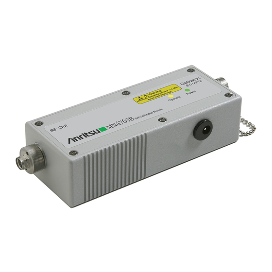
RF connector. The Warning label indicates that the maximum optical input power to the MN4765B is 10 mW or 10 dBm. Exceeding this value will cause damage to the internal photodiode. Figure 2-1. -
Page 11: Power Requirements
Figure 2-1. MN4765B O/E Calibration Module (2 of 2) Power Requirements The MN4765B AC power adapter accepts 100 VAC to 240 VAC, 50 Hz to 60 Hz, single-phase power. The calibration module is intended for Installation Category (Over Voltage Category) II. -
Page 12: Mn4765B Measurement Setup
De-embedding O/E Standard Figure 2-2. MN4765B E/O Measurement Setup With a VectorStar VNA 1. Connect the MN4765B RF OUT port to Port 2 of the VNA (Other models of VNA can be used, but this will change the available frequency range). - Page 13 2-4 Preparation for Use 2. Connect Port 1 of the MS4647B to the RF Input port of the modulator. 3. Connect the output port of the modulator to the Optical In port on the MN4765B. O/E Module MN4765B OM PN: 10410-00742 Rev. H...
- Page 14 2-4 Preparation for Use Installation PN: 10410-00742 Rev. H O/E Module MN4765B OM...
-
Page 15: Chapter 3-Operation
Chapter 3 — Operation Introduction This chapter provides information on the operation of the MN4765B O/E Calibration Module. The illustrations provided for Vector Network Analyzer connections use the Anritsu VectorStar VNA as an example. Other Anritsu VNAs use similar connections, but the resulting performance data will be slightly different. -
Page 16: Required Equipment
Figure 3-1 on page 3-3 appears. Follow the instructions to load the 12-term electrical calibration. 3. Load the s2p characterization file of the MN4765B. This removes the response of the photodiode that will be used for the E/O measurement. PN: 10410-00742 Rev. H... - Page 17 Operation 3-2 E/O Measurements Figure 3-1. E/O Measurement Dialog 4. Connect the modulator DUT to the MN4765B photodiode in series as shown in Figure 2-2 on page 2-4. To achieve the maximum signal level at the input of the photodiode, a polarization controller is recommended to adjust Note the polarization of the laser input to the modulator DUT.
-
Page 18: Measurement Tips
• Polarization Maintaining Fiber (PMF) is an easy way to minimize polarization changes as a result of fiber turns and bends. The transfer function measurement of a 40 Gb/s modulator using the Anritsu VectorStar VNA is shown in Figure 3-2. - Page 19 DUT. A representation of phase linearity through the device can be obtained by removing the fixed electrical length. The Anritsu VNA's reference plane adjustment can be used to compensate for the phase change over frequency to display the variation from linear phase.
-
Page 20: O/E Measurements
Once the response of the modulator is removed, the S21 parameter displays the ratio of the output electrical signal to the input optical modulated signal. Transfer Function Measurement of a MN4765B Module using the VectorStar VNA is shown in Figure 3-3 Figure 3-4. - Page 21 Operation 3-3 O/E Measurements The 3 dB bandwidth can be determined from the measurement using the Anritsu VectorStar VNA; approximately 53 GHz in the Option 70 example shown above in Figure 3-3 on page 3-6, and approximately 95 GHz in the...
-
Page 22: Required Equipment
From the O/E-E/O menu, select O/E Measurements. 3. Follow the instructions in the dialog shown in Figure 3-5 to load the 12-term electrical calibration that was saved in Step 1. Figure 3-5. O/E Measurement Dialog PN: 10410-00742 Rev. H O/E Module MN4765B OM... - Page 23 4. After entering the s2p file for the characterized modulator, the VNA is now calibrated and ready to make O/E measurements. Connect the characterized modulator and detector under test as shown in Figure 2-2 on page 2-4. O/E Module MN4765B OM PN: 10410-00742 Rev. H...
-
Page 24: O/O Measurements
O/O normalization calibration step. In any event, at the conclusion of the process, the reference planes are both in the optical domain and an O/O annunciator will be displayed. Figure 3-6. O/O Measurement Dialog 3-10 PN: 10410-00742 Rev. H O/E Module MN4765B OM... -
Page 25: Appendix A-Supplemental Information
• When asked to load the original cal file, select the calibration that was saved in Step 1. 3. After loading the VNA calibration, load the s2p file for the MN4765B. 4. Connect the optical components together as shown in... - Page 26 8. The screen should now display S21 (magnitude and phase) for the E/O modulator. The data can then be stored as an s2p file by selecting File, Save Data and by appropriately setting the file format and naming the file. PN: 10410-00742 Rev. H O/E Module MN4765B OM...
-
Page 27: Optical Measurement Considerations
For example, a modulator with an FC/PC connector at the output will require an optical patch cord to adapt to the FC/APC connector on the input of the MN4765B. Optical fibers have negligible frequency dependent loss over the modulation bandwidths... -
Page 28: Modulator Bias Control
RF signal linearly modulates the optical carrier. Note that when an MBC is applied, it must be designed for small signal operation. The default power of the Anritsu VNA providing 70 GHz is such that most commercial modulators will be well within their small signal regime with the VNA’s drive level. - Page 29 Supplemental Information A-2 Optical Measurement Considerations O/E Module MN4765B OM PN: 10410-00742 Rev. H...
- Page 31 Anritsu Company Anritsu utilizes recycled paper and environmentally conscious 490 Jarvis Drive inks and toner. Morgan Hill, CA 95037-2809 http://www.anritsu.com...
Need help?
Do you have a question about the MN4765B and is the answer not in the manual?
Questions and answers