Table of Contents
Advertisement
Quick Links
Advertisement
Table of Contents

Related Manuals for Alpha Data ADM-XRC-9R1


Summary of Contents for Alpha Data ADM-XRC-9R1
- Page 1 ADM-XRC-9R1 User Manual Document Revision: 1.7 16th Sept 2020...
- Page 2 ADM-XRC-9R1 User Manual V1.7 - 16th Sept 2020 © 2020 Copyright Alpha Data Parallel Systems Ltd. All rights reserved. This publication is protected by Copyright Law, with all rights reserved. No part of this publication may be reproduced, in any shape or form, without prior written consent from Alpha Data Parallel Systems Ltd.
-
Page 3: Table Of Contents
ADM-XRC-9R1 User Manual V1.7 - 16th Sept 2020 Table Of Contents Introduction ............................1 Key Features ..........................1 Order Code ............................ 2 References & Specifications ......................2 Installation ............................3 Hardware Installation ........................3 2.1.1 Handling Instructions ......................... 3 2.1.2 Motherboard / Carrier Requirements .................. - Page 4 LED Locations ........................... 7 Figure 3 JTAG Boundary Scan Chain ......................9 Figure 4 On-Board Digital System Clocks ..................... 10 Figure 5 MGT Clocks ............................. 11 Figure 6 ADM-XRC-9R1 RF sampling clock ....................12 Figure 7 CPLD Connections .......................... 14...
- Page 5 Figure 11 MGT Links ............................18 Figure 12 PL DRAM Banks ..........................19 Figure 13 GPIO Block Diagram ........................19 Figure 14 Front Panel IO ..........................20 Figure 15 ADM-XRC-9R1 ADC Performance ....................22 Figure 16 ADM-XRC-9R1 DAC Performance ....................23...
- Page 6 ADM-XRC-9R1 User Manual V1.7 - 16th Sept 2020 Page Intentionally left blank...
-
Page 7: Introduction
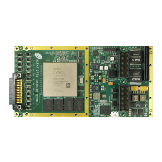
ADM-XRC-9R1 User Manual V1.7 - 16th Sept 2020 1 Introduction The ADM-XRC-9R1 is a high-performance XMC for applications using Zynq Ultrascale+ RFSoC from Xilinx. 1.1 Key Features Key Features • Single-width XMC, compliant to VITA Standard 42.0, 42.3 and 42.10d12 •... -
Page 8: Order Code
= air cooled industrial Cooling /CC1 = conduction cooled industrial Table 1 : Build Options Not all combinations are available. Please check with Alpha Data sales for details. 1.3 References & Specifications ANSI/VITA 42.0 XMC Standard, December 2008, VITA, ISBN 1-885731-49-3 ANSI/VITA 42.2... -
Page 9: Installation
- Store in ESD safe bag. 2.1.2 Motherboard / Carrier Requirements The ADM-XRC-9R1 is a single width XMC.3 mezzanine with P6 and P4 connectors. The motherboard/ carrier must comply with the XMC.3 (VITA 42.3) specification for the Primary XMC connector, J5. -
Page 10: Cooling Requirements
The power dissipation of the board is highly dependent on the Target FPGA application. A power estimator spreadsheet is available on request from Alpha Data. This should be used in conjunction with Xilinx power estimation tools to determine the exact current requirements for each power rail. -
Page 11: Functional Description
ADM-XRC-9R1 User Manual V1.7 - 16th Sept 2020 3 Functional Description 3.1 Overview Figure 1 : ADM-XRC-9R1 Block Diagram Functional Description Page 5 ad-ug-1353_v1_7.pdf... -
Page 12: Switch Definitions
ADM-XRC-9R1 User Manual V1.7 - 16th Sept 2020 3.1.1 Switch Definitions There is a set of eight DIP switches placed on the rear of the board. Their functions are described in Switch Definitions. Note: SW1-5 and SW1-8 are OFF by default. Factory Configuration switch must be in the OFF position for normal operation. -
Page 13: Led Definitions
Pin low Table 4 : LED Definitions 3.1.2.1 User LEDs The user LEDs are attached to the CPLD and use an SPI interface to control them. The ADM-XRC-9R1 reference design provides VHDL code to control this interface. Functional Description Page 7... -
Page 14: Xmc Platform Interface
ADM-XRC-9R1 User Manual V1.7 - 16th Sept 2020 3.2 XMC Platform Interface 3.2.1 IPMI I2C A 2 Kbit I2C EEPROM (type M24C02) is connected to the XMC IPMI. This memory contains board information (type, voltage requirements etc.) as defined in the XMC based specification. -
Page 15: Jtag Interface
ADM-XRC-9R1 User Manual V1.7 - 16th Sept 2020 3.3 JTAG Interface 3.3.1 On-board Interface A JTAG boundary scan chain is connected to header U12. This allows the connection of the Xilinx JTAG cable for FPGA debug using the Xilinx ChipScope tools. -
Page 16: Clocks
V1.7 - 16th Sept 2020 3.4 Clocks The ADM-XRC-9R1 provides a wide variety of clocking options. The board has a user-programmable clock generator. These clocks can be combined with the FPGA's internal PLLs to suit a wide variety of communication protocols. -
Page 17: Pn6 Reference Clock (Pn6_Pcierefclk)
ADM-XRC-9R1 User Manual V1.7 - 16th Sept 2020 3.4.3 PN6 Reference Clock (PN6_PCIEREFCLK) The reference clock "PN6_PCIEREFCLK" is a differential clock provided by a carrier card through the Secondary XMC connector P6 at pins A19 and B19. This board connects this pair to an MGT clock input. -
Page 18: Digital System Oscillators
3.4.7 RF Sampling Clocks The RF reference clocks are generated with a dual-loop jitter cleaner PLL. The RF sampling clocks are provided by three LMX2594 RF clock synthesisers. Figure 6 : ADM-XRC-9R1 RF sampling clock Signal Frequency Target FPGA Input "P"... -
Page 19: Sysref Clocks
ADM-XRC-9R1 User Manual V1.7 - 16th Sept 2020 3.4.7.1 Sysref Clocks The sysref clocks provide the sysref functionality to synchronize the RF DACs and ADCs. They are provided by the RF clock generators. They are connected to the PL and the RF sampling block. -
Page 20: Rf Clock Programming
ADM-XRC-9R1 User Manual V1.7 - 16th Sept 2020 3.4.7.3 RF Clock Programming The RF reference clocks are programmed from the PL using SPI (LMX2594) or uWire (LMK04208). To minimise FPGA IO pin usage, a CPLD is used to multiplex a single 4-wire IO interface to the FPGA to each of the 4 devices. -
Page 21: Zynq Ps Block
3.5.4 PS DDR4 Memory The ADM-XRC-9R1 is fitted with one bank of PS DDR4 SDRAM. The bank is made up of a two 16-bit wide memory devices in parallel to provide a 32-bit datapath capable of running up to 1200MHz (DDR4-2400). 8Gbit devices (Micron MT40A512M16HA-083) are fitted as standard to provide 2GByte of memory. -
Page 22: Ethernet Interfaces
Ports. The default speed of the COM ports is 115.2k. COM2 uses RS-232 by default but may be configured for RS-485 operation. Please contact Alpha Data for further details of the RS-485 mode. COM0 and COM2 are both connected to PS UART1, and are therefore mutually exclusive due to the PS only having two UART interfaces. -
Page 23: Usb Interfaces
V1.7 - 16th Sept 2020 3.5.8 USB Interfaces The ADM-XRC-9R1 has two external USB interfaces connected to rear connector P4. The Zynq PS is configured as the USB host to the external interfaces. The on-board system monitor is accessible from the micro-USB connector... -
Page 24: Interfaces
The Target FPGA IO is arranged in banks, each with their own supply pins. The bank numbers, their voltage and function are shown in Target FPGA IO Banks. Full details of the IOSTANDARD required for each signal are given in the ADM-XRC-9R1 example design. IO Banks Voltage Purpose 3.3V... -
Page 25: Memory Interfaces
V1.7 - 16th Sept 2020 3.6.3 Memory Interfaces The ADM-XRC-9R1 has two independent banks of DDR4 SDRAM. Each bank consists of one 8-bit wide memory device capable of running at up to 1200MHz (DDR-2400). 8Gbit devices (Micron MT40A1G8PM-083E) are fitted as standard. -
Page 26: Rf Interfaces
The default configuration for the DAC is to operate in 20mA mode, with 2.5V DAC_AVTT). It is possible to run in 32mA mode, with 3.3V DAC_AVTT. Please contact Alpha Data for further details if this is required. The ADC voltages in the table below are the single ended voltages at the RF connector. The DAC voltages are the voltages driving a 50 Ohm impedance. -
Page 27: Table
ADM-XRC-9R1 User Manual V1.7 - 16th Sept 2020 Signal Impedance (Ohms) J2 pin number DAC1 DAC2 DAC3 DAC4 DAC5 DAC6 DAC7 REF IN REF OUT EXTIO0 EXTIO1 Table 18 : Front panel I/O signals Functional Description Page 21 ad-ug-1353_v1_7.pdf... -
Page 28: Rf Performance
ADC measurements were taken over the range 50MHz to 3990MHz, and DAC measurements over the range 50MHz to 3190MHz. For all DACs/ADCs the result is adjusted to 0dB at 50MHz. Figure 15 : ADM-XRC-9R1 ADC Performance Page 22 Functional Description... -
Page 29: Figure 16 Adm-Xrc-9R1 Dac Performance
ADM-XRC-9R1 User Manual V1.7 - 16th Sept 2020 Figure 16 : ADM-XRC-9R1 DAC Performance Functional Description Page 23 ad-ug-1353_v1_7.pdf... -
Page 30: Configuration
Monitoring. 3.9 System Monitoring The ADM-XRC-9R1 has the ability to monitor temperature and voltage to maintain a check on the operation of the board. The monitoring is implemented using the Atmel AVR microcontroller. Control algorithms within the microcontroller automatically check line voltages and on board temperatures and shares the information with the PS. -
Page 31: Automatic Temperature Monitoring
ADM-XRC-9R1 User Manual V1.7 - 16th Sept 2020 3.9.1 Automatic Temperature Monitoring At power-up, the control logic sets the temperature limits and resets the LM87's over-temperature interrupt. The temperature limits are shown in Table Temperature Limits: FPGA Board Commercial 0 degC... -
Page 32: System Monitor Interfaces
3.9.3 System Monitor Interfaces There are two ways to communicate with the System Monitor to retrieve board status information on the ADM-XRC-9R1. One is through the Micro USB connector (shown in Interfaces), the other is using one of the PS UART interfaces (shown in Serial COM Ports). -
Page 33: Appendix A Rear Connector Pinouts
ROOT0_L Table 23 : Pn5 Interface *FPGA pins MRSTO_L and MBIST_L are disconnected by default (with MRSTO_L pulled high with a pullup resistor). Please contact Alpha Data for further details if this is required. Rear Connector Pinouts Page 27 ad-ug-1353_v1_7.pdf... -
Page 34: Secondary Xmc Connector, P6
ADM-XRC-9R1 User Manual V1.7 - 16th Sept 2020 Appendix A.2: Secondary XMC Connector, P6 PN6_TX_P0 PN6_TX_N0 P6_USB1_DP PN6_TX_P1 PN6_TX_N1 P6_COM1_RXD P6_USB1_DM P6_COM1_TXD PN6_TX_P2 PN6_TX_N2 P6_USB1_VBUS PN6_TX_P3 PN6_TX_N3 P6_COM2_TXP P6_USB2_DP P6_COM2_TXN PN6_TX_P4 PN6_TX_N4 P6_USB2_DM PN6_TX_P5 PN6_TX_N5 P6_COM2_RXP P6_USB2_VBUS P6_COM2_RXN PN6_TX_P6 PN6_TX_N6... -
Page 35: Pn6 Gpio Pin Map
GP18 Table 25 : Pn6 GPIO Pin Map *FPGA pins K10 and K12 can optionally drive MRSTO# and MBIST# on the XMC P5 connector. Please contact Alpha Data for further details if this is required. Rear Connector Pinouts Page 29... -
Page 36: Pmc Connector P4
ADM-XRC-9R1 User Manual V1.7 - 16th Sept 2020 Appendix A.3: PMC Connector P4 Signal P4 Pin P4 Pin Signal P4_ETH0_MDI_0_P P4_ETH0_MDI_2_P P4_ETH0_MDI_0_N P4_ETH0_MDI_2_N P4_ETH0_MDI_1_P P4_ETH0_MDI_3_P P4_ETH0_MDI_1_N P4_ETH0_MDI_3_N P4_ETH1_MDI_0_P P4_ETH1_MDI_2_P P4_ETH1_MDI_0_N P4_ETH1_MDI_2_N P4_ETH1_MDI_1_P P4_ETH1_MDI_3_P P4_ETH1_MDI_1_N P4_ETH1_MDI_3_N P4_USB1_DM P4_USB2_DM P4_USB1_DP P4_USB2_DP P4_USB1_VBUS... -
Page 37: Table
ADM-XRC-9R1 User Manual V1.7 - 16th Sept 2020 Revision History Date Revision Nature of Change Initial Draft. 22 Jul 2019 First Release. 30 Jul 2019 Updated block diagram to show 2x Ethernet phys, added 03 Dec 2019 section about programming the RF clock synthesisers. - Page 38 ADM-XRC-9R1 User Manual V1.7 - 16th Sept 2020 Page Intentionally left blank Address: Suite L4A, 160 Dundee Street, Address: 611 Corporate Circle, Suite H Edinburgh, EH11 1DQ, UK Golden, CO 80401 Telephone: +44 131 558 2600 Telephone: (303) 954 8768...
Need help?
Do you have a question about the ADM-XRC-9R1 and is the answer not in the manual?
Questions and answers