Table of Contents
Advertisement
Quick Links
Alpha Data XRM-IO146
I/O Interface Connector for ADM-XRC-5T1 Image/
Video Processing Module
A l l t r a d e m a r k s , b r a n d n a m e s , a n d b r a n d s a p p e a r i n g h e r e i n a r e t h e p r o p e r t y o f t h e i r r e s p e c t i v e o w n e r s .
• C r i t i c a l a n d e x p e d i t e d s e r v i c e s
• I n s t o c k / R e a d y - t o - s h i p
Artisan Scientific Corporation dba Artisan Technology Group is not an affiliate, representative, or authorized distributor for any manufacturer listed herein.
In Stock
Used and in Excellent Condition
Open Web Page
https://www.artisantg.com/63354-1
• We b u y y o u r e x c e s s , u n d e r u t i l i z e d , a n d i d l e e q u i p me n t
• F u l l - s e r v i c e , i n d e p e n d e n t r e p a i r c e n t e r
Advertisement
Table of Contents

Related Manuals for Alpha Data ADM-XRC-5T1


Summary of Contents for Alpha Data ADM-XRC-5T1
- Page 1 Alpha Data XRM-IO146 I/O Interface Connector for ADM-XRC-5T1 Image/ Video Processing Module In Stock Used and in Excellent Condition Open Web Page https://www.artisantg.com/63354-1 A l l t r a d e m a r k s , b r a n d n a m e s , a n d b r a n d s a p p e a r i n g h e r e i n a r e t h e p r o p e r t y o f t h e i r r e s p e c t i v e o w n e r s .
- Page 2 ADM-XRC-5T1 User Manual Revision: 2.2 Date: 2nd April 2012...
- Page 3 All rights reserved. This publication is protected by Copyright Law, with all rights reserved. No part of this publication may be reproduced, in any shape or form, without prior written consent from Alpha Data Parallel Systems Limited. Head Office US Office...
-
Page 4: Table Of Contents
2.2 Motherboard / Carrier requirements ......................... 2 2.3 PCI Mode selection ............................2 2.4 Installing the ADM-XRC-5T1 onto a PMC motherboard................... 2 2.5 Installing the ADM-XRC-5T1 if fitted to an ADC-PMC ..................2 2.6 Cooling Requirements............................3 3 Software Installation ............................4 4 Board Description ............................... - Page 5 ADM-XRC-5T1 User Manual (v2.2 - 2nd April 2012) 4.8.3 XRM Interface - MGT Links........................20 4.9 Pn4 I/O ................................21 4.9.1 Pn4 Signalling Voltage ..........................22 4.10 XMC Interface ..............................23 4.10.1 Primary XMC Connector ......................... 23 4.11 XRM IO146 Interface............................24 4.12 XRM HSSDC2A Interface..........................
-
Page 6: Introduction
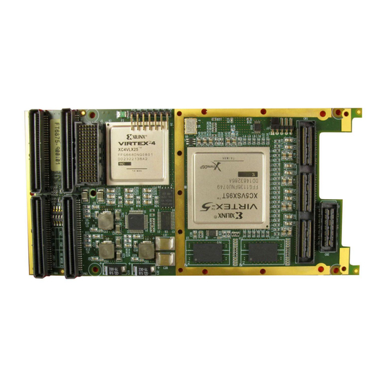
(v2.2 - 2nd April 2012) 1 Introduction The ADM-XRC-5T1 is a high performance PCI Mezzanine Card (PMC) designed for applications using the Virtex™-5 FPGAs from Xilinx. This card supports VIrtex-5 LX110T, LX155T, SX95T and FX70T devices with the FFG1136 package. -
Page 7: Hardware Installation
The ADM-XRC-5T1 is a 3.3V only PCI device and is not compatible with systems that use 5V signalling. The ADM-XRC-5T1 must be installed in a PMC motherboard or carrier that supplies +5.0V and +3.3V power to the PMC connectors. Ensure that this requirement is satisfied before powering it up. +12V and -12V may also be required for certain XRM modules. -
Page 8: Cooling Requirements
(v2.2 - 2nd April 2012) It should be noted that the ADC-PMC uses a standard bridge to provide a secondary PCI bus for the ADM-XRC-5T1 and that some older BIOS code does not set up these devices correctly. Please ensure you have the latest version of BIOS appropriate for your machine. -
Page 9: Software Installation
(v2.2 - 2nd April 2012) 3 Software Installation Please refer to the SDK installation CD. The SDK contains drivers, examples for host control and FPGA design and comprehensive help on application interfacing. Page 4 Software Installation Alpha Data Parallel Systems Ltd. ad_ug01159... -
Page 10: Board Description
(v2.2 - 2nd April 2012) 4 Board Description The ADM-XRC-5T1 follows the architecture of the ADM-XRC series and decouples the "target" FPGA from the PCI interface, allowing user applications to be designed with minimum effort and without the complexity of PCI design. -
Page 11: Local Bus
4.2 Local Bus The ADM-XRC-5T1 implements a multi-master local bus between the bridge and the target FPGA using a 32- or 64-bit multiplexed address / data path. The bridge design is asynchronous and allows the local bus to be run faster or slower than the PCI bus clock to suit the requirements of the user design. -
Page 12: Flash Memory
ADM-XRC-5T1 User Manual (v2.2 - 2nd April 2012) 4.3 Flash Memory The ADM-XRC-5T1 is fitted with two separate Flash memories: one connected to the Bridge / Control FPGA and the other to the User FPGA. 4.3.1 Board Control Flash A 256Mb Flash memory (Intel / Numonyx PC28F256P30) is used for storing Vital Product Data (VPD), programmable clock parameters and configuration bitstreams for the User FPGA. -
Page 13: One-Time Configuration (Otc)
4.4 Health Monitoring The ADM-XRC-5T1 has the ability to monitor temperature and voltage to maintain a check on the operation of the board. The monitoring is implemented by a National Semiconductor LM87 and is supported by the Bridge FPGA control logic using I2C. - Page 14 +3V3 Reading = 3.32 V +5V Reading = 5.04 V Pn4 Reading = 3.31 V FPIO Reading = 3.34 V SysMon Int Temp = 33 deg. C User FPGA Temp = 26 deg. C Board Description Page 9 ad_ug01159 Alpha Data Parallel Systems Ltd.
-
Page 15: Automatic Temperature Monitoring
SCAN chain is initialised. The JTAG Header pinout is shown in Figure 6, "JTAG Header J2": Figure 6: JTAG Header J2 The scan chain is shown in Figure 7, "JTAG Boundary Scan Chain": Page 10 Board Description Alpha Data Parallel Systems Ltd. ad_ug01159... -
Page 16: Jtag Voltage
FPGA if one is present. Shorting FBS to the adjacent GND pin will disable this process and can be used to recover situations where rogue bitstreams have been stored in flash. Board Description Page 11 ad_ug01159 Alpha Data Parallel Systems Ltd. -
Page 17: Clocks
ADM-XRC-5T1 User Manual (v2.2 - 2nd April 2012) 4.6 Clocks The ADM-XRC-5T1 is provided with numerous clock sources, as shown in Figure 8, "Clock Structure" below: RefClk PCI-X Zero-delay Buffer Bridge Config (PLL) (Coolrunner) Bridge FPGA (V4LX25) XTAL_CLK REFCLK_200M 25.0 MHz... -
Page 18: Refclk
In order to make use of the IODELAY features of Virtex™-5, a stable low-jitter clock source is required to provide the base timing for tap delay lines in each IOB in the User FPGA. The ADM-XRC-5T1 is fitted with a 200MHz LVPECL (LVDS optional) oscillator connected to global clock resource pins. -
Page 19: Xrm Regional Clocks
80MB/s. The ADM-XRC-5T1 can be configured to boot the User FPGA from flash on power-up if a valid bit-stream is detected in the flash. Booting from flash will also configure the programmable clocks. See Section 4.3.1.1, "Power-Up Sequence"... -
Page 20: I/O Bank Voltages
4.7.3 Memory Interfaces 4.7.3.1 DDRII SDRAM The ADM-XRC-5T1 has two independent banks of DDRII SDRAM. Each bank consists of two memory devices in parallel to provide a 32 bit datapath. 1Gb Micron MT47H64M16-3 devices are fitted as standard to provide 256MB per bank. The board supports 2Gb devices and these are available as an ordering option. -
Page 21: Xrm Bus And Front Panel I/O
The signalling voltage on the XRM connector (and User FPGA Banks 12, 18, 20 & 22) is selectable by jumper J3. XRM I/O voltage Link p1 & p2 3.3V Link p2 & p3 2.5V Link p3 & p4 2.5V Link p5 & p4 1.8V Table 8: XRM I/O Voltage Selection Page 16 Board Description Alpha Data Parallel Systems Ltd. ad_ug01159... -
Page 22: Xrm Interface - Standard Signals And Power
AD10 CLK0 +3.3V AD11 CLK1 +3.3V XRM_SERID +3.3V RESERVED XRM_VREF XRM_VCCIO VBAT XRM_VCCIO +12V XRM_VCCIO +12V -12V PRESENCE_L XRM_TDI XRM_TCK XRM_TRST XRM_TMS XRM_TDO Table 9: XRM Interface - part 1 Board Description Page 17 ad_ug01159 Alpha Data Parallel Systems Ltd. -
Page 23: Table 10: Xrm Interface - Part 2
CLK3 CLK4 N_34 CLK5 P_34 N_33 CLK6 P_33 CLK7 S_10 XRM_CLKIN_N XRM_MGTREF_P XRM_CLKIN_P XRM_MGTREF_N XRM_SDA XRM_PECL_N XRM_SCL XRM_PECL_P RESERVED XRM_TX7_P XRM_RX7_P XRM_TX7_N XRM_RX7_N Table 10: XRM Interface - part 2 Page 18 Board Description Alpha Data Parallel Systems Ltd. ad_ug01159... -
Page 24: Table 11: Xrm Interface - Part 3
N_54 P_53 P_54 P_55 N_56 N_55 P_56 N_57 N_58 P_57 P_58 N_59 N_60 P_59 P_60 N_61 N_62 P_61 P_62 N_63 N_64 P_63 P_64 Table 11: XRM Interface - part 3 Board Description Page 19 ad_ug01159 Alpha Data Parallel Systems Ltd. -
Page 25: Xrm Interface - Mgt Links
XRM_TX5_P XRM_TX5_N 120A XRM_RX5_P XRM_RX5_N XRM_TX6_P XRM_TX6_N 124B XRM_RX6_P XRM_RX6_N XRM_TX7_P (CN1) 117 XRM_TX7_N (CN1) 119 124A XRM_RX7_P (CN1) 118 XRM_RX7_N (CN1) 120 Table 12: XRM Interface - MGT Links Page 20 Board Description Alpha Data Parallel Systems Ltd. ad_ug01159... -
Page 26: Pn4 I/O
K34 [CC] J34 [CC] PN4_N24 PN4_P25 J32 [CC] PN4_P26 PN4_N25 H33 [CC] PN4_N26 PN4_P27 PN4_P28 PN4_N27 PN4_N28 PN4_P29 PN4_P30 PN4_N29 PN4_N30 PN4_P31 PN4_P32 PN4_N31 PN4_N32 Table 13: Pn4 to FPGA Assignments Board Description Page 21 ad_ug01159 Alpha Data Parallel Systems Ltd. -
Page 27: Pn4 Signalling Voltage
It should be noted that the switch does not directly route power. The switch position is monitored by the board control logic which, in turn, sets a power multiplexer to use either 2.5V or 3.3V. Page 22 Board Description Alpha Data Parallel Systems Ltd. ad_ug01159... -
Page 28: Xmc Interface
PCIE_TX3_P PCIE_TX3_N 122B PCIE_RX3_P PCIE_RX3_N PCIE_TX4_P PCIE_TX4_N 118A PCIE_RX4_P PCIE_RX4_N PCIE_TX5_P PCIE_TX5_N 118B PCIE_RX5_P PCIE_RX5_N PCIE_TX6_P PCIE_TX6_N 114A PCIE_RX6_P PCIE_RX6_N PCIE_TX7_P PCIE_TX7_N 114B PCIE_RX7_P PCIE_RX7_N Table 15: XMC J1 Connections Board Description Page 23 ad_ug01159 Alpha Data Parallel Systems Ltd. -
Page 29: Xrm Io146 Interface
N_22 P_23 P_24 N_23 N_24 P_25 P_26 N_25 N_26 P_27 P_28 N_27 N_28 P_29 P_30 N_29 N_30 Table 17: IO146 Mictor Connector Pins 39 - 76 (continued on next page) Page 24 Board Description Alpha Data Parallel Systems Ltd. ad_ug01159... -
Page 30: Io146 Mictor Connector Pins 77 - 114
N_50 P_51 P_52 N_51 N_52 P_53 P_54 N_53 N_54 P_55 P_56 N_55 N_56 P_57 P_58 N_57 N_58 Table 19: IO146 Mictor Connector Pins 115 - 152 (continued on next page) Board Description Page 25 ad_ug01159 Alpha Data Parallel Systems Ltd. -
Page 31: Io146 Mictor Connector Pins 115 - 152
Mictor Pin Samtec FPGA Pin Signal P_59 P_60 N_59 N_60 P_61 P_62 N_61 N_62 P_63 P_64 N_63 N_64 CLK6 S_10 CLK7 Table 19: IO146 Mictor Connector Pins 115 - 152 Page 26 Board Description Alpha Data Parallel Systems Ltd. ad_ug01159... -
Page 32: Xrm Hssdc2A Interface
P1-2 102B XRM_RX0_N CN2-4 P1-3 XRM_RX1_P CN2-6 P2-2 102A XRM_RX1_N CN2-8 P2-3 XRM_RX2_P CN2-18 P3-2 103B XRM_RX2_N CN2-20 P3-3 XRM_RX3_P CN2-22 P4-2 103A XRM_RX3_N CN2-24 P4-3 Table 20: XRM-HSSDC2A-5T2 Pinout Board Description Page 27 ad_ug01159 Alpha Data Parallel Systems Ltd. - Page 33 DCI_CASCADE usage. Other minor updates and corrections. 02-04-2012 4.9: Corrected bank number for the Pn4 signals. ©2012 Alpha Data Parallel Systems Ltd. All rights reserved. All other trademarks and registered trademarks are the property of their respective owners. Address: 4 West Silvermills Lane,...
Need help?
Do you have a question about the ADM-XRC-5T1 and is the answer not in the manual?
Questions and answers