Sign In
Upload
Manuals
Brands
Alpha Data Manuals
Control Unit
ADM-XRC-9R1
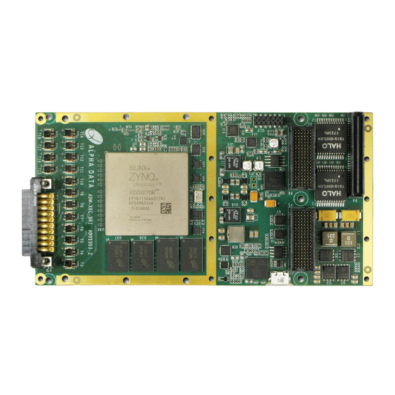
Alpha Data ADM-XRC-9R1 Manuals
Manuals and User Guides for Alpha Data ADM-XRC-9R1. We have
1
Alpha Data ADM-XRC-9R1 manual available for free PDF download: User Manual
Alpha Data ADM-XRC-9R1 User Manual (38 pages)
Brand:
Alpha Data
| Category:
Control Unit
| Size: 1 MB
Table of Contents
Table of Contents
3
1 Introduction
7
Key Features
7
Order Code
8
References & Specifications
8
Build Options
8
References
8
2 Installation
9
Hardware Installation
9
Handling Instructions
9
Motherboard / Carrier Requirements
9
Cooling Requirements
10
3 Functional Description
11
Overview
11
Figure 1 ADM-XRC-9R1 Block Diagram
11
Switch Definitions
12
LED Definitions
13
User Leds
13
Figure 2 LED Locations
13
XMC Platform Interface
14
Ipmi I2C
14
Mbist
14
Mvmro
14
Mrsti
14
Mrsto
14
Mpresent
14
JTAG Interface
15
On-Board Interface
15
XMC Interface
15
JTAG Voltages
15
Figure 3 JTAG Boundary Scan Chain
15
Clocks
16
300Mhz Reference Clocks (REFCLK300M and FABRIC_CLK)
16
Pcie Reference Clocks (PCIEREFCLK)
16
Table 5 REFCLK300M Connections
16
Table 6 PCIEREFCLK Connections
16
Figure 4 On-Board Digital System Clocks
16
PN6 Reference Clock (PN6_PCIEREFCLK)
17
Programmable Clocks (PROGCLK 0-2)
17
MGT Reference Clocks
17
Table 7 PN6_PCIEREFCLK Connections
17
Table 8 PROGCLK Connections
17
Figure 5 MGT Clocks
17
Digital System Oscillators
18
RF Sampling Clocks
18
Reference Clocks Connections
18
Figure 6 ADM-XRC-9R1 RF Sampling Clock
18
Table 10 RF Clock Connections
18
RF System FPGA Reference Clock
19
Sysref Clocks
19
Table 11 Sysref Connections
19
Table 12 FPGA Reference Clock Connections
19
Figure 7 CPLD Connections
20
RF Clock Programming
20
Table 13 FPGA 4-Wire Connections
20
Zynq PS Block
21
Boot Modes
21
Quad SPI Flash Memory
21
Microsd Flash Memory
21
PS DDR4 Memory
21
PS MGT Links
21
Table 14 Boot Mode Selection
21
Ethernet Interfaces
22
Serial COM Ports
22
Table 15 Ethernet Status Leds
22
Figure 8 Ethernet Interfaces
22
Figure 9 Serial COM Ports
22
USB Interfaces
23
Figure 10 USB Interfaces
23
Interfaces
24
I/O Bank Voltages
24
MGT Links
24
Table 16 Target FPGA IO Banks
24
Table 17 Target MGT Links
24
Figure 11 MGT Links
24
Memory Interfaces
25
Gpio
25
Figure 12 PL DRAM Banks
25
Figure 13 GPIO Block Diagram
25
RF Interfaces
26
Front-Panel I/O
26
Table
26
Table 18 Front Panel I/O Signals
26
Figure 14 Front Panel IO
26
Table
27
RF Performance
28
Figure 15 ADM-XRC-9R1 ADC Performance
28
Figure 16 ADM-XRC-9R1 DAC Performance
29
Configuration
30
Power-Up Sequence
30
System Monitoring
30
Table 19 Voltage and Temperature Monitors
30
Automatic Temperature Monitoring
31
Microcontroller Status Leds
31
Table 20 Temperature Limits
31
Table 21 Status LED Definitions
31
System Monitor Interfaces
32
Table 22 Avr2Util Clock Indexes
32
Appendix A Rear Connector Pinouts
33
Primary XMC Connector, P5
33
Table 23 Pn5 Interface
33
Secondary XMC Connector, P6
34
Table 24 Pn6 Interface
34
Pn6 GPIO Pin Map
35
Table 25 Pn6 GPIO Pin Map
35
PMC Connector P4
36
Table 26 Pn4 Interface
36
Table
37
Advertisement
Advertisement
Related Products
Alpha Data ADM-XRC-5T1
Alpha Data ADM-XRC-5T2-ADV
Alpha Data ADM-XRC-II
Alpha Data ADM-XRC-II Pro
Alpha Data ADM-XRC-7Z2
Alpha Data ADM-XRC-7V1
Alpha Data ADM-XRC-7Z1
Alpha Data ADM-XRC-9R4
Alpha Data ADM-XRC-9R1B
Alpha Data ADM-XA210
Alpha Data Categories
Computer Hardware
PCI Card
Control Unit
Motherboard
Adapter
More Alpha Data Manuals
Login
Sign In
OR
Sign in with Facebook
Sign in with Google
Upload manual
Upload from disk
Upload from URL