
Subscribe to Our Youtube Channel
Related Manuals for GW Instek GFG-80150


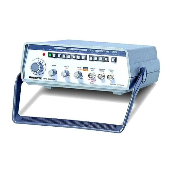
Summary of Contents for GW Instek GFG-80150
- Page 2 TABLE OF CONTENTS PAGE SECTION 1 ..26 PAGE GENERAL DESCRIPTION ..27 Power Supply ..26 · .. · · INTRODUCTION · · · · · · 27 Summing Amphfier • M E CHANICAL DESCRIPTION . . 1 · · · .27 Inverter Case/Top and Bottom Covers ..
- Page 3 LIST OF ILLUSTRATONS PAGE PAGE Fig. Controls and Indicators ........ . Fig. Removal of Multiplier Knob ....Triangle Waveform ........Alignment of Multiplier Knob ......Fig. Unsymmetrical Triangle (Ramp) Waveform ..Fig. Block Diagram ........ Diode Shaping Bridge .........
- Page 4 SECTION 1 GENERAL DESCRIPTION INTRODUCTION Front Panel The Function Generator provides square, triangle, sine, ramp The main output and a l l controls are located on the front and pulse waveforms over a frequency range of 0.2Hz panel. They are: the pu,hbutton POW E R switch, power ON puis a VCF (voltage controlled frequency) input, 2MHz, indicator, seven frequency RANGE pushbutton switches,...
- Page 5 SPECIFICATIONS ELECTRICAL DESCRIPTION Specifications are listed below in table 1-1. Test procedures lor The FUNCTION GENERATOR utilize two constant current verification of specification are given in Section 3. sources of opposite polarity lor charging and discharging a timing capacitor to produce the triangular waveform. Table 1-1 Specifications A diode shaping bridge netwrok shapes the triangle to produce the low-distoriton sine wave.
- Page 6 Power Output (50r!ll Waveforms - Since, triangle, square, ± Requirements: pulse and ramp Amplitude - >20Vpp open circuit lOOV, 120V, 220V, 230V AC >l OVpp into 50!1 10%, 50/60 Hz. Approx. 5 watts. Attenuation - 20db continuously var iable plus 20db for the output Physical DC Offset - (variable) Char acteri sties:...
- Page 7 SECTION 2 INSTAL LATION AN D O PERATION From figure 5-2 select the jumper or jumpers correspond· UNPACKING A N D INSPECTION ing to the desired line voltage of operation . Remo ve the jumper or jumpers previously installed in the The FUNCTION GENERATOR are packaged to absorb any P.C.
- Page 8 A.ANGE FUNCTION r...; �""\,. . -20dB � I 100K INPUT OUTPLIT OUTPUT PULSE DUTY OFFSET Controls and Indicators 2 - 1 Fig.
- Page 10 NOTE: The time symmetry as illustrated below is for refer· ence only. Any desired time symmetry ratio may be set as desired within the limits as described in Section 4, DUTY. Pulse Ramp/Pulse MAIN OUTPUT Duty Square Sine Output Triangle Invert Switch Control '1...
- Page 11 9 AMPLITUDE OFFSET (PULL A DJ) DC OFFSET control is provided to allow the DC level of A MPLITUDE control provides 20db of attenuation of the OUTPUT waveforms to be set as desired. the output waveform selected by the FUNCTION switch. NOTE: The amount of offset plus the amplitude setting cannot exceed the maximum amplitude or clipping will...
- Page 13 DUTY CONTROL In other words, the pulse width equals one-half the time per iod of the frequency set by the RANGE and M U LTIPLIER Wh i le observing the triangle waveform on the oscil l oscope, controls. rotate the DUTY control CW from the CAL position. The time symmetry of the Sine wave may be set in the same Observe one slope of the triangle remains constant while the manner, providing additional versatility.
- Page 15 Set controls as indicated below for all accuracy checks unless indicated otherwise in each table. POWER RANGE REFER TO TABLES MULT. REFER TO TABLES INVERT NORM (OUT) FUNCTION DUTY CAL (MAX CCW) DC O F F SET AMPLITU DE MAX (MAX CW) - 12 -...
- Page 16 Table 3-2 Frequency Accuracy Time Frequ ency Period F re q ue nc y Toleranc e T i me Toleranc e R ang e M u l t. Period R e a ding Readin g 52632 to .4 7 6 1 9 p se c 2.
- Page 17 Table Freauencv Accraoy (Continued) Range Frequency Reading Frequency Tolerance Time Period Reading Time Period Tolerance 1 1 00.0 to 900.00KHz 1.0000 Jlsec 1 . 1 1 1 1 to . 90909 J1Sec 1000 OOK Hz 110.00 to 90.000K Hz 1 OO.OOOK Hz 1 0.
- Page 18 Frequency Range Table 3-3 R ange Multip l ier Frequenc y Toleran c e Time Period Tol era nc e >2 . 000 M Hz < 5 000 1.1 sec <2 0 < 2 000H z >5. 000 se c FREQUENCY COUNTER SET FOR SQUARE WAVE MAX OUTPUT 0 0 0...
- Page 19 Table VCF (Voltage Controlled Frequency) VC F Frequency Tolerance Time Period Reading Voltage Voltage Mult I nput Range Reading 5 .0 JlSeC ±5 % ± 2 5 0 MV 2 00KHz ± !llb lOOK ± 5 % 2 00Hz ±5% 5.
- Page 21 Table 3-6 D. C. Offset (Main Output) Range Mult Function Amplitude D C Offset Oulput Voltage To lerance 2. 0 Max CW + > 1 0 VDC Open Ckt Max CCW - >-lOVDC Open Ckt "v Min (CCW) Max CW + >-5VDC into 5011 Load Max CCW - >-5VDC into 50(1 Load...
- Page 22 Table 3-7 Sine Distortion Sine D istort i on Toleranc e Function R ange Mult 2. 0 l OOK . 2 0 2 . 0 1 0 K 2 .0 .2 0 2. 0 <1 % Sin e Dis to rtion "v .2 0 2 .
- Page 23 Table Sine Distortion (Continued) HARMONIC DISTORTION ANALYZER IC: ::= == =: :: :: :il [ 0 0 (i) OUT PUT SPECTRUM ANALYZER INPUT - 2 0 �-...
- Page 24 Table Sine Frequency Response Range Mult Amplitude Sine Amplitude Tolerance ± Measured Value Mea-.ured Va (+1.15%) lOOK Max CW OSCILLU�COPt Measured Value (±5.92%) ____ ---- 0 on Usc 50S2 terrnrniltrcn on oscrlloscore rnput...
- Page 25 Ta!Jie 3-9 Square Wave Rise and Fall Time Range Mult Ampliturle Function Rise Time Fall Time Square Aberrations <±5% of pp Amp or -±:0.5 lOOK lOV pp <1 OOns <lOOns OSCtL LOSCOPE_ l'lJ r Us� 50D trrnw>Jt1cn on oscilloscope input - 22 -...
- Page 26 3� Table Pulse Output Nominal Pulse Output load R i se Time Fall Time Pulse Amp l itude Nominal Range Mull Rise T ime/Fall Time Tolerance 1 Ons >+3V Open C ircuit <25ns <.BV l OOK TTL Loads >2.0V 1Sns 131rl Res From Pulse <25ns <...
- Page 28 Unsymm etrical Triangle (Ramp) Waveform Fig. A TTL GATE is also driven by the square wave from the LEVEL DETECTO R . The output of the TTL GATE provides a TTL pulse at the PULSE output connector . A diode shaping bridge network uses the log curve of sil icon diod�s to simulate a sinusoidal curve.
- Page 29 C I RCUIT DESC R I PTION (Main Generator! Summing Amplifier The power supply shown in the Block Diagram, figure 6·1, U201 is an operational amplifier. 0201 is an emitter follower consists of a f u l l wave unregulated ±20V supply and a re buffer used in conjunction with the operational amplifier.
- Page 30 Negative Current Source to increase three decades or to the maximum frequency in Positive and dicated on the seiPcted frequency RANGE. By setting the The positive and negative current sources provide a constant MULTIPLIER at the desired start f requency and applying the current for charging and discharging the timing capacitors.
- Page 34 feedback from the output emitter followers thru to the R507 base of 0502 maintains output signal approximately 1 0 times the input signal. As the i nput signal becomes negative. 0501 collector current decreases and 0502 collector current increases. As 0502 collector current i ncreases, the current from 0503 collector becomes less than the current from 0504 and the output follows the input negative.
- Page 35 SECTION 5 MAINTENANCE bration becomes necessary. DISASSEMBLY FOR CALI BRATION Remove the four retaining screws located on the bottom Equipment Required cover which secure the bottom cover, figure. 5-1. The equipment required for caJibrat1on is listed in table Push up on the four tabs from which the retaining screws were removed to loosen the cover.
- Page 36 M P A D J + 1 5.5V A DJ S I N E IIISCD .. ICl 110111 MAlliS IU,Lf 1 11011 UPU.CIJI(; JII S I. ® o Q o fiOI &1 - lll)'; i,, > _ ,� •0 S I N E llOV ;...
- Page 37 main OUTPUT. Set the horizontal sweep rate of the to the Procedure oscilloscope to 0.5ms em. all controls as follows unless otherwise indicated: POWER Adjust SYM and SYM 8 to one complete symmetri· Range-Hz obtain cal triangle the CRT (10cm). across MULTIPL I ER INVERT...
- Page 39 T able 5-1 Troubleshooting Procedure Reference Circuit Test Point Probable Cause Signal Symptom Page N o . t20V ± 5V + 20V - 20V -20V + 5V + 1 5V + 1 5V No Power Power Supply No Power - 1 5V - 1 5V ±...
- Page 40 Table 5- 1 Troubleshooting Procedure (Continued} Circuit Symptom Probable Cause Test Point Signal Reference Page No. 0203 Emitter +9 V DC 0204 Emitter. -9 VDC 0 20 1 Collector +9 VDC 0202 Collector -9 VDC No output Generator Loop Current Sources 0201 Emitter + 2 .2 VDC "V ±...
- Page 41 Reference Test Point Signal Symptom Probable Cause Circuit Page No '"\/ R 4 1 7 2Vpp R 4 1 2 1 50mv P P No Sine wave, OV ± 250mv Faulty Camp Sine Amplifier 28 29 R401 2Vpp Triangle & Square Ok S501A NO 2Vpp...
- Page 42 Place the M U L T I P L I E R knob and dial skirt on the shaft MULTI P LI E R A L I G N M E N T PROC E D U R E with 2.0 on the dial skirt directly i n l i ne with the index 5-4.
- Page 43 1 2 0VAC POWE R SUPPLY I N V E: 11 T RAMP/PULSE v-2ov +20Vt 1 5 V .- - - - - ""b M I N G SINE POS I T ! V E S I N E C U R R E N T l E A U401 .a,.
- Page 44 CIFICU IT OIAGFIANI '"'' lOOk +15. 5 -J5.5V -IS_SV I • AI.OUI1t0 Mil l.&tiOAY Alit IU. UAN;! lo.j,OQyi CIICUIIn MIMPVI NDIICI fU� IUINIR :1 11111\41(1 w•11 Rllll l u•.C11ANCI "' UNliU ' ..�,·· , . , , , , , "...
- Page 45 CII'ICUIT OIAOAAM 1" 15 5V R503 -15 5V A:ll6 IClSk 1.2K R319 5 1 K RJ20� :' E � J ti � l. ACU 5_.,lCI O UT . ,, -IS �y...
- Page 47 MAINTENANCE The following instructuions are use for by qualified only. To avoid electrical shock, do not perform any servicing other than contained in the operating instructions unless you are qualified to do so. 1 . FUSE Replacement: li the fuse bolws, the FUNCTION GENERATOR will not operate. Try to determine and correct the cause of the blown fuse , then replace only with a fuse of the correct rating and type, as shown below.
- Page 48 EC Declaration of Conformity GOOD WILL INSTRUMENT CO., L TD. ( I ) N0.7 - I , Jhongsing Road, Tuchcng City. Taipei County 236, Taiwan N0.69,Lu Shan Rd.,New District,Suzhou City,P.R.C. declare under sole responsibil ity that GFG-8015G Are herewith confirmed to comply with the requirements set out in the Council Directive on the Approximation of the Law of Member States relating to Electromagnetic Compatibility (89/336/EEC,921J 1 /EEC, 93/68/EEC) and Low Voltage Equipment Directive (73/23;FEC).
Need help?
Do you have a question about the GFG-80150 and is the answer not in the manual?
Questions and answers