Advertisement
Quick Links
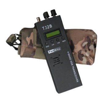
CONSTRUCTION OF TJ2B HANDHELD SSB TRANSCEIVER
The TJ2B is a high-performance QRP portable multi-band SSB transceiver using DDS as
the LO, and offering wide frequency coverage and fine tuning rate.
The Doubly Balanced
Diode Ring Mixer makes strong signal handling capability possible. The TJ2B is a
pre-assembled kit. You need only assemble a few parts and connect some cables to be
qrv.
Operating Frequency: 3 - 18.2 MHz (Kit A)
Mode: LSB, USB, CW (RX)
Tuning Rate: 1Hz, 10Hz, 100Hz, 1KHz, 10KHz, 100KHz
IF: 9 MHz
Sensitivity: 0.3uV
Current Drain: 260 mA (RX)
Operating Power: 10 - 13.6V
Output Power: 5W
40 Memories
Dual VFO
Memory-VFO Transfer
Advertisement

Subscribe to Our Youtube Channel
Related Manuals for YouKits TJ2B


Summary of Contents for YouKits TJ2B
- Page 1 CONSTRUCTION OF TJ2B HANDHELD SSB TRANSCEIVER The TJ2B is a high-performance QRP portable multi-band SSB transceiver using DDS as the LO, and offering wide frequency coverage and fine tuning rate. The Doubly Balanced Diode Ring Mixer makes strong signal handling capability possible. The TJ2B is a pre-assembled kit.
- Page 2 Tuning steps of 1 Hz are available. Pressing the TUNE knob selects the tuning rate. Included Hardware: Buttons, switches, DC sockets, earphone socket, pot, and encoder. A miniature speaker is packed in the bottom cover of the enclosure.
- Page 3 Cables for internal connections Components package...
- Page 4 Toroids Note: FB-43-2401 may be supplied in the kit. This core is larger than FT-43-37. Can Inductors...
- Page 5 Pre-assembled Miniature Transformers (Packed in a separate plastic bag) Brass Stand-Off Parts...
- Page 6 Included DC cable as a free gift. All the SMD have been assembled in the factory. However, some bulkier components, such as the buttons,switches, can transformers, toroids, electro caps., have not been assembled. Thess components prone to damage in transpiration if they were pre-assembled.
- Page 7 1. DDS Unit Assemble the following components: (C34 has no component) 1) Assemble Y1, the 2MHz crystal. Bend the leads before soldering. Otherwise it will be too high. 2) Assemble MIC. Notice the Ground pin (the pin connected to the casing). Solder the GND pin of the MIC to the GND pad of CN6 (the square pad on the left), and solder the MIC pin to the MIC pad (the round pad).
- Page 8 3) Assemble the 3.5mm stereo socket to J1. This is the external MIC and PTT socket. Because of the manufacturing process, the top cover opening for J1 cannot be lower. It is suggested to modify the socket a little so as to align with the opening better. It takes only 2 or 3 minutes.
- Page 9 4) Solder a 220uF electrolytic capacitor to C7 pads. (C7 may have been assembled). 5) Solder a miniature transformer to T1 pads. Six such transformers are supplied in the bag. Use one of them here. Insert the LCD cable to the FFC socket (CN3). Do not assemble the buttons until the LCD is assembled.
- Page 10 How to insert the LCD Cable Never bend the cable end soldered to the LCD!
- Page 11 Now carefully insert the flat cable into the socket. When the cable is inserted into position, press the lock bar down to lock the cable. Never bend the cable end which is soldered to the LCD PCB. This will break the cable at the end, because the thin tracks have no protecting plastic at the end.
- Page 12 Now, solder the 7-wire cable.
- Page 13 Supply 12V from the 7-pin cable, negative to "GND", positive to “+12V". Voltage ranging from 10.5 - 13.8V works. Never connect the wrong polarity! When the power is connected, the backlight is on. There may be nothing seen on the LCD screen at first. Don't worry. Adjust the contrast control VR1, until the display appears.
- Page 14 Solder the 5-pin socket to CN2. This is the encoder and tuning rate port. Assemble CN2 at the other side of the PCB, making it easier to run the cable. Pins 1 - 3 are soldered to encoder pins 1 - 3 respectively. Pins 4 - 5 are soldered to the two encoder switch pins.
- Page 15 9) Solder the MIC cable to CN5. Use the yellow connector. Note: The square pad (on the right) is GND, the round pad is the MIC pad. They are routed to the MIC pad and the GND pad of Main board CN4 respectively. 10) Assemble the SETUP switch which is on the PCB back.
- Page 16 GND clip to GND of DDS Unit. The reading should be 12.000.000. This is the display frequency + IF (9.000.000). If there is no reading, check T1 for a cold solder joint. The reading may be not accurate, around 12 MHz, because of the 100 MHz crystal tolerance.
- Page 17 alter the value to 2800, so that LSB and USB are 1.4 kHz from the center frequency. Press the MEM button to save the modified data. Press SETUP to exit. Monitor the frequency meter. Tune from 3 - 18.199999 MHz using LSB mode, the reading is always 9 MHz higher than the DDS LCD displays.
- Page 18 6) Two TQ2 relays (Notice the bar printed on the relay. There is also a bar printed on the PCB.) 7) 220uF electrolyte caps. Note: The longer lead is "+". Solder them to C28, C30,C80,C82 pad. Find “+” on the PCB. Never mistake the polarity.
- Page 19 Notice "+" symbol. 8) Solder the 9 MHz crystals on main board Y1 - Y5 pads. 9) Solder the can inductors to the main board. The can without any number is for T4; the can labeled (3) is for L2; and the can labeled (2) is for L3.
- Page 20 10) Solder T1, T2, T3, T5, T6. These are miniature transformers. One of them is used on the DDS Unit. 11) Assemble the 10k trimmer on the CN2 pads. Adjust the leads so that they fit the pads.
- Page 21 12) Assemble VC1 Notice the mounting direction of this variable cap. 13) Solder the 10uF chip at C27 if a capacitor is not already present. Notice the polarity. The brown bar is "+". If the SMT chip is too small for you to handle, you can use an ordinary electrolytic cap here instead.
- Page 22 14) Assemble L1, L12, L13, L14, L15. L1 - Colour code inductor Now, wind the coils : Use 0.42 emaneled wire supplied in the kit. The emanel of 0.42 wire is a kind of solder aid. You don't have to scrape the emanel. Tin the leads directly. The emanel melts when heated.
- Page 23 16) Assemble T7. Broadband transformer, 5 bifilar turns 0.31 enameled wire on the binocular core made up of 2 small sleeves. Cut a pair of 12 cm long enameled wires, and thread through the core. 1 - 2 is wire A; 3 - 4 is wire B. Connect 2 (the finish of wire A) with 3 (the start of wire B) as the tap (Use Ohm meter to identify each wire).
- Page 24 T7 is soldered on the 3-lead pads, with the tap in then middle pad. No connection on the 2-pin lpads.
- Page 25 Another picture of T7 17) Assemble T8. Broadband transformer, 5 bifilar turns on FT37-43 core, 0.42 wire. Cut 2 pieces of 15 cm long enameled wires, wire A and wire B. Twist the 2 wires before winding. Connect 2 (the finish of wire A) with 3 (the start of wire B) as the tap (Use an Ohm meter to identify).
- Page 26 18) Assemble the bias resistor of the power transistor R62. 19) Assemble D18 on then PCB back. Solder a 100 ohm resistor on the leads of D18, i.e., the resistor is paralleled with D18. 20) Put a jump wire in JP3.
- Page 27 21) Jump JP1 and JP2 with a hookup wire (JP1 is near J3. JP2 is near J2). Jump these two points on the PCB back. 22) Next construct the power transistor assembly. First bent the transistor leads. Put the insulating bush into the transistor heat sink mounting hole.
- Page 28 Use an Ohm meter to check the resistance between the aluminum and the power transistor heat sink (collector). There should be no reading. If the reading is 0 ohms, this indicates a short circuit between the transistor and the aluminum plate. Check the insulating bush.
- Page 29 Use two 2 mm spring washers for each screw. The thickness of the 2 stacked springs is almost that of the speaker rim. Place 2 spring washers, and then a shim. Lock with the nut.
- Page 30 Cut the 2-wire ribbon cable in appropriate length (a length of 90 mm is enough) and solder the 2-wire cable to the speaker pads. Assemble the black connector to the cable. Assemble the DDS Unit to the enclosure. The stands-off are pre-made inside the enclosure.
- Page 31 Place the DDS Unit in position. The screen and the buttons fit the opennings. Press the buttons. They should be running-fit. Tighten the assembly with 4 10mm stands-off. Use 1 washer and 1 spring washer, so that the stand-off is raised 1mm. Tighten the stand-off.
- Page 32 togather as one tail, but the screen would be too hard to handle. tin the leads and solder to DDS CN4 and MAIN CN1, center inductor to the center hole, screen to the any 2 holes of the the 4 holes. Solder the 3-wire cable to the AF GAIN 10k pot.
- Page 33 The GND pin goes to the GND pad (square pad). Assemble the blue connector, and plug the cable to CN3. 3. Testing the Rig Five components need adjusting. They are T4, L2, VC1, 10k variable on CN2, and L3. Pug the 7-pin ribbon cable to CN5, speaker cable to CN6. Plug in the encoder. The MIC cable is not very long.
- Page 34 Do not assemble the power transistor assembly to the main board now. 2) Connect 12V DC to J3, or to J2. Never plug in the wrong polarity! The center pin is "+". Move the power switch to EXT position (external power). If you use J2 as input , move to BATT position (battery).
- Page 35 50 ohm cable and MIC cable are connected. How the cable is soldered.
- Page 36 Now connect the antenna. Set AF GAIN to 1/3 or 1/4 level. Tune to 7MHz, adjust T4 to peak the recieved signal. Rotate the TUNE knob, you can hear ham signals, and other radio stations. If you are testing the rig in the evening, at 5MHz, you can pick up the beacon signal.
- Page 37 See how to arrange the 5-wire ribbon cable.
- Page 38 Fasten the encoder, AF GAIN POT, ANT socket to the top cover, but do not assemble the cover to the enclosure. Slantly slide in the main board, with the power switch handle aligned with the opening on the side.
- Page 39 The enclosuer side wall blocks the main board a little, because of the DC12V socket. Pull the enclosure edge, and press the main board at the same time, so that the main board goes into the enclosure. The ANT socket tail may be a little longer. Cut the tail to fit the space. Fasten the cover to the enclosure walls.
- Page 40 Don't forget to solder ANT leads. Assemble the two brass stands-off with a tai to the mounting holes.
- Page 41 Assemble the power transistor assembly to the main board , with the power transistor leads in the pads. Fasten the aluminium to the stands-off. You can solder the 3 leads easily. No screws are needed in the 2 top mounting holes. Now, put on the PTT button.
- Page 42 Assemble the bottom cover. The last step. How to place the battery? The battery pack (optional) is placed on the back cover, with 2 pieces of adhesive tape. It...
- Page 43 is also a good practice to placea piece of tape near the connector. Cut the leads short if they are too high above the main board back, such as the can inductor leads, CN4 leads. Stick 3 or 4 pieces of thicker tape on the main board. Place a piece of thin hard card between the tape and the battery to prevent it from touching the main board.
- Page 44 BNC- Antenna socket MIC- External microphone and PTT. For better performance, use an external MIC. Note: Always turn off the power before plugging in the external MIC. The tip is MIC, the narrow ring is PTT, and the inner conductor is GND. AF GAIN- Volume control.
- Page 45 sequence is 1Hz, 10Hz, 100Hz, 1kHz, 10kHz, and 100kHz. 2) Buttons: MOD- Mode switch. Press to select LSB, USB and CW (RX) A / B- VFO Selection /Memory clearing. Press to select VFO A or VFO B. In MEM state, hold the button until all of the memories are cleared.
- Page 46 PTT- Push to talk. Press to transmit. DC12V- External power socket 5. Miscellaneous Bias resistor R62- This resistor depends on the specific power transistor and D18. supplied resistor is 680 ohms. LCD Holder - Sink the 2 mounting screws (screen side) as deep as possible. Otherwise the LCD could not reach the position.
- Page 47 6. Dis-assemble the rig You may want to improve the kit, or the kit needs repair some day. You have to open the enclosure and take out the main board. Dis-assemble the kit reverse operation. 1) Pull out the PTT button. Remove the screws and open the back cover. 2) Remove the two screws to fasten the aluminum plate.
- Page 48 Now, the main board is up from one side, ready to be pulled out. 7. DC cable- The wire labled white dash is the center, i.e., "+"; the other "-". However, please use the ohm meter to confirm. The bush should be connected to "-", the center to "+", never use the wrong polarity!
- Page 49 8. KIT B Notes Construction of KIT B is the same, except the following: 1) L3 is not necessary. No. 2 can inductor is not supplied in the kit; 2) C50 is a pre-assembled cap; 3) T8 - Broadband transformer, 4 turns; 4) L12, L13 - 15m LPF inductor, 10 turns;...
- Page 50 10. Simple Way to Calibrate L3 A much easier way to calibrate L3 is to tune the frequency to 8.998000MHz with antenna connected, and adjust L3 until the received noise weakest, i.e., to suppress the received signal. Use 100 KHz tuning rate to get to that frequency faster. While you tune from 3 MHz - 8.998000 MHz, you may notice a sudden mute (received noise level drops suddenly), this silence is where the trap works.
- Page 51 11. Troubleshooting and Repair “I noticing that the TJ2B receive sound is not as loud. So I took the back cover off and when I touch the board and depress, it becomes loud again.” This is caused by two possible reseasons on the main board: 1) Cold solder of T1, T2, T3.
- Page 52 2) Select proper gate time Several gate time buttons appear on the panel: 0.01s, 0.1s, 1s, etc. Which button should be used? In our case, "1s" button is to be used to obtain the reading in "Hz". 10MHz and 100MHz buttons are for CH1. Use 10MHz button since the DDS output frequency is 12.000000MHz.
- Page 53 (Different frequency counter has different warming-up time. Consult the instruction for the correct warming-up time). Turn on TJ2B.Let it run for 10 - 20 minutes for the clock to stabilize. Connect the red alligater clip to the center of the DDS output cable, the black alligater clip to the ground (the cable bread).
- Page 54 Press MEM to save the calibration. Exit SETUP.Now you can setup the IFS and USB compensation. Some users may say, my frequency counter reading is 12000.002, some may 11999.997. This result is good enough, because the room temperature, the accuracy of the frequency counter contribute to the result.
- Page 55 Do not worry. About 10 - 20 minutes the frequency will be 8998.400 again. According to the experiment, it takes about 15 minutes for the BFO to stablize at the ambient temperature of 30°C. The BFO crystal needs warming-up time. Let TJ2B work for 15 - 20 minutes before Calibrating the BFO frequency.
- Page 56 Tj2B is used with the advanced DDS as LO, the frequency is accurate, rock-stable; the signal pure and clean, the tuning fast and smooth. However, the the accuracy of the DDS depends on the precise calibration of the DDS clock. A good frequency counter is required for this process.
Need help?
Do you have a question about the TJ2B and is the answer not in the manual?
Questions and answers