
Subscribe to Our Youtube Channel
Related Manuals for VIA Technologies EPIA-M910


Summary of Contents for VIA Technologies EPIA-M910
- Page 1 USER MANUAL VIA EPIA-M910 Highly-integrated Mini-ITX board with rich feature set and multiple expansion options 1.08-03052020-153600...
- Page 2 VIA Technologies, Inc. reserves the right the make changes to the products described in this manual at any time without prior notice. Regulatory Compliance FCC-A Radio Frequency Interference Statement This equipment has been tested and found to comply with the limits for a class A digital device, pursuant to part 15 of the FCC rules.
- Page 3 Battery Recycling and Disposal Only use the appropriate battery specified for this product. Do not re-use, recharge, or reheat an old battery. Do not attempt to force open the battery. Do not discard used batteries with regular trash. ...
- Page 4 VIA EPIA-M910 User Manual Box Contents 1 x VIA EPIA-M910 board 1 x SATA cable 1 x SATA power cable (for DC-in SKU only) 1 x DC power cable (for DC-in SKU only) 1 x I/O bracket...
-
Page 5: Table Of Contents
VIA EPIA-M910 User Manual Table of Contents 1. Product Overview ........................1 1.1. Key Features and Benefits ........................... 1 1.1.1. VIA Nano ® X2 E-Series/Eden ® X2/QuadCore E-Series CPU .............. 1 1.1.2. VIA VX900 MSP Chipset ..........................1 1.1.3. Modular Expansion Options ........................2 1.2. - Page 6 VIA EPIA-M910 User Manual 5. Hardware Installation ........................ 49 5.1. Installing into a Chassis .............................49 5.1.1. Suggested Minimum Chassis Dimensions .....................49 5.1.2. Suggested Minimum Chassis Height ......................50 5.1.3. Suggested Keepout Areas ........................50 6. BIOS Setup Utility ........................51 6.1. Entering the BIOS Setup Utility ........................51 6.2.
- Page 7 VIA EPIA-M910 User Manual 6.9. Advanced Chipset Settings ..........................67 6.9.1. North Bridge VIA VX900 Configuration ....................67 6.9.1.1. DRAM Clock/Timing Configuration .....................68 6.9.1.1.1. DRAM Clock ..........................68 6.9.1.2. OnChip VGA Configuration ......................69 6.9.1.2.1. Select Display Device 1 and 2 ....................69 6.9.1.2.2.
- Page 8 VIA EPIA-M910 User Manual B.3.8. EuP/ErP Enable S3 ............................87 B.3.9. EuP/ErP Enable Power OFF .........................87 B.4. EPIA-M910-10PE ..............................88 B.4.1. Playing DVD – Power DVD 5.0 ........................88 B.4.2. Playing MP3 – Media Player ........................88 B.4.3. Running Network Application ........................88 B.4.4. IDLE ..................................88 B.4.5.
- Page 9 Figure 3: External I/O port dimensions of the VIA EPIA-M910 ...................7 Figure 4: Height distribution ...............................8 Figure 5: Height distribution of the VIA EPIA-M910 (for EPIA-M910-10E & EPIA-M910-10PE) ......9 Figure 6: Back panel I/O ports ............................10 Figure 7: PS/2 port diagram .............................. 11 Figure 8: VGA port diagram .............................
- Page 10 VIA EPIA-M910 User Manual Figure 57: Illustration of ACPI Configuration screen ....................57 Figure 58: Illustration of APM Configuration screen ....................58 Figure 59: Illustration of Spread Spectrum Configuration screen ................61 Figure 60: Illustration of USB Configuration screen ....................62 Figure 61: Illustration of CRB Configuration screen ....................
- Page 11 VIA EPIA-M910 User Manual List of Tables Table 1: Layout diagram description table of the VIA EPIA-M910 ................6 Table 2: Layout diagram description table of the back panel I/O ports ............... 10 Table 3: PS/2 port pinouts ............................... 11 Table 4: VGA port pinouts ............................... 11 Table 5: COM port pinouts ..............................
-
Page 12: Product Overview
Technology Suite, and VIA TwinTurbo technology. The VIA EPIA-M910 has two DDR3 1066 DIMM slots that support up to 8GB memory size. The VIA EPIA- M910 provides support for high fidelity audio with its included VIA VT2021 High Definition Audio Codec. -
Page 13: Modular Expansion Options
The VIA EPIA-M910 enable companies to slowly roll out upgrades as necessary instead of having to replace everything all at once. This ensures that companies using the VIA EPIA-M910 obtain the maximum benefits from its past investments in PCI expansion cards. -
Page 14: Product Specifications
VIA EPIA-M910 User Manual 1.2. Product Specifications Processor 1.6GHz VIA Nano ® X2 E-Series (with fan) 1.0GHz VIA Eden ® X2 (fanless) 1.2GHz VIA QuadCore E-Series (with fan) Chipset VIA VX900 Media System Processor ... - Page 15 VIA EPIA-M910 User Manual Back Panel I/O 2 x COM ports (powered with selectable 5V/12V) 1 x VGA port ® 1 x HDMI port 2 x Gigabit Ethernet ports 4 x USB 2.0 ports ...
-
Page 16: Layout Diagram
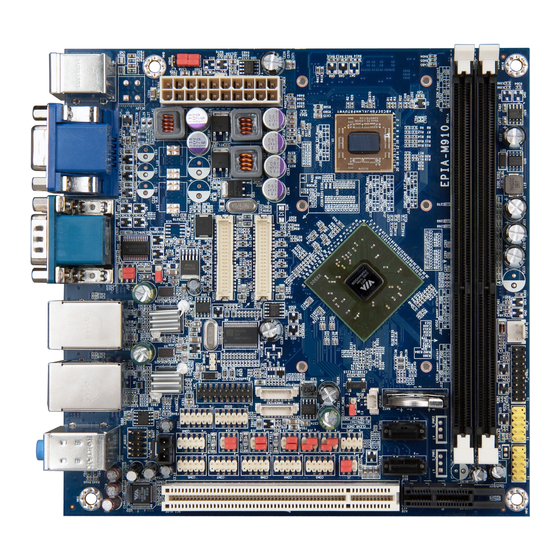
VIA EPIA-M910 User Manual 1.3. Layout Diagram VIA CP U VX 900 Figure 1: Layout diagram of the VIA EPIA-M910 (top view) Item Description DC-in power connector (DC12V1) * for DC-in SKU only PS/2 keyboard and mouse pin header (KBMS) -
Page 17: Table 1: Layout Diagram Description Table Of The Via Epia-M910
Front panel pin header (F_PANEL) USB 2.0 pin headers (USB_1 and USB_2) JATX_on mode jumper (JATX_ON) Table 1: Layout diagram description table of the VIA EPIA-M910 Note: For the purposes of simplifying the illustration, the connectors for both DC-in and ATX Power versions have... -
Page 18: Product Dimensions
VIA EPIA-M910 User Manual 1.4. Product Dimensions Unit: mm Figure 2: Mounting holes and dimensions of the VIA EPIA-M910 Unit: mm Figure 3: External I/O port dimensions of the VIA EPIA-M910... -
Page 19: Height Distribution
VIA EPIA-M910 User Manual 1.5. Height Distribution Unit:mm Figure 4: Height distribution Note: Diagram (Figure 4) shows the height distribution of VIA EPIA-M910 (for EPIA-M910-16, EPIA-M910-16P, EPIA- M910-12Q & EPIA-M910-12PQ) -
Page 20: Figure 5: Height Distribution Of The Via Epia-M910 (For Epia-M910-10E & Epia-M910-10Pe)
VIA EPIA-M910 User Manual Unit:mm Figure 5: Height distribution of the VIA EPIA-M910 (for EPIA-M910-10E & EPIA-M910-10PE) Note: All other heights are under 21.00mm. -
Page 21: I/O Interface
VIA EPIA-M910 User Manual 2. I/O Interface The VIA EPIA-M910 has a wide selection of interfaces, and includes a selection of frequently used ports as part of the external I/O coastline. 2.1. External I/O Ports Figure 6: Back panel I/O ports... -
Page 22: Ps/2 Port
2.1.1. PS/2 Port The VIA EPIA-M910 has two integrated PS/2 ports for keyboard and mouse. Each port is using the 6-pin Mini-DIN connector. The color purple is used for a PS/2 keyboard while the color green is used for a PS/2 mouse. -
Page 23: Com Port
VIA EPIA-M910 User Manual 2.1.3. COM Port The integrated 9-pin COM port uses a male DE-9 connector. The COM (COM1) port supports the RS-232 standard. The pinouts of the COM port are shown below. Figure 9: COM port diagram Signal... -
Page 24: Audio Jack
VIA EPIA-M910 User Manual 2.1.5. Audio Jack There are three audio jack receptacles integrated into a single stack on the I/O coastline. Each receptacle can fit a 3.5mm Tip Ring Sleeve (TRS) connector to enable connections to Line-in, Line-out, and Mic-in. -
Page 25: Usb 2.0 Port
VIA EPIA-M910 User Manual 2.1.7. USB 2.0 Port The VIA EPIA-M910 is equipped with two USB 2.0 ports which gives complete Plug and Play and hot swap capability for external devices. The USB 2.0 interface complies with USB UHCI, Rev. 2.0. The pinouts of the USB 2.0 port are shown below. -
Page 26: Onboard I/O
2.2. Onboard I/O 2.2.1. ATX Power Connector The VIA EPIA-M910 has a 20-pin ATX power connector onboard. The ATX power connector is labeled as “ATX_POWER1”. The pinouts of the ATX power connector are shown below. Figure 14: ATX power connector diagram... -
Page 27: Lvds Panel Connectors
VIA EPIA-M910 User Manual 2.2.2. LVDS Panel Connectors The VIA EPIA-M910 has two LVDS panel connectors: LVDS1 and LVDS2. LVDS1 connector is controlled by VIA VX900 chipset while the LVDS2 connector is controlled by VT1636 LVDS transmitter. The pinouts of the LVDS panel connectors are shown below. -
Page 28: Table 13: Lvds2 Panel Connector Pinouts (Dual-Channel)
VIA EPIA-M910 User Manual Signal Signal PVDD2 -A4_L PVDD2 A4_L -A5_L -A0_L A5_L A0_L -A6_L -A1_L A6_L A1_L -CLK2_L -A2_L CLK2_L A2_L -A7_L -CLK1_L A7_L CLK1_L -A3_L A3_L DISPCLKI0 DISPCLKO0 Table 13: LVDS2 panel connector pinouts (dual-channel) Signal Signal PVDD2... -
Page 29: Lvds Inverter Connectors
VIA EPIA-M910 User Manual 2.2.3. LVDS Inverter Connectors The VIA EPIA-M910 has two inverters for controlling the LVDS panel backlight and brightness. INVERTER1 corresponds to the LVDS1 panel connector. INVERTER2 corresponds to the LVDS2 panel connector. The pinouts of the LVDS inverter connectors are shown below. -
Page 30: Digital I/O Pin Headers
VIA EPIA-M910 User Manual 2.2.4. Digital I/O Pin Headers The VIA EPIA-M910 includes two Digital I/O pin headers that supports eight GPO and eight GPI pins. The pinouts of the Digital I/O pin headers are shown below. Figure 17: Digital I/O pin headers diagram... -
Page 31: Dc-In Power Connector
VIA EPIA-M910 User Manual 2.2.5. DC-in Power Connector For the DC version of the VIA EPIA-M910, there is a DC-in power connecter in addition to the DC-in coaxial power connector. This enables two methods for delivering +12V to the VIA EPIA-M910. The pinouts of the DC-in power connector are shown below. -
Page 32: Sata Power Connectors
VIA EPIA-M910 User Manual 2.2.6. SATA Power Connectors For the DC version of the VIA EPIA-M910, there are two built-in SATA power connectors. These connectors are required to power SATA hard drives. The SATA power connectors are labeled as “S_PWR1” and “S_PWR2”. The pinouts of the SATA power connectors are shown below. -
Page 33: Cmos Battery Slot
VIA EPIA-M910 User Manual 2.2.7. CMOS Battery Slot The VIA EPIA-M910 is equipped with a CMOS battery slot, which is compatible with CR2032 coin batteries. The CMOS battery slot is labeled as “BAT2”. When inserting a CR2032 coin battery, be sure that the positive side is facing the locking clip. -
Page 34: Front Panel Pin Header
VIA EPIA-M910 User Manual 2.2.8. Front Panel Pin Header The front panel pin header consists of 15 pins in a 16-pin block. Pin 15 is keyed. The front panel pin header is labeled as “F_PANEL1”. It provides access to system LEDs, power, reset, system speaker and HDD LED. -
Page 35: Smbus Pin Header
VIA EPIA-M910 User Manual 2.2.9. SMBus Pin Header The SMBus pin header consists of three pins that allow connecting the SMBus devices. The devices communicate with a SMBus host and/or other SMBus devices using the SMBus interface. It is labeled as “SMBUS”. -
Page 36: Cpu And System Fan Connectors
VIA EPIA-M910 User Manual 2.2.10. CPU and System Fan Connectors There are two fan connectors on board: one for the CPU and one for the chassis. The fan connector for the CPU is labeled as “CPUFAN1” and the fan connector for the system is labeled as “SYSFAN1”. The fans provide variable fan speeds controlled by the BIOS. -
Page 37: Sata Connectors
VIA EPIA-M910 User Manual 2.2.11. SATA Connectors The two SATA connectors on board can support up to 3Gbps transfer speeds. The SATA connectors are labeled as “SATA1” and “SATA2”. The pinouts of the SATA connectors are shown below. Figure 24: SATA connectors diagram Note: To use the SATA Disk-on-Module flash drive on the board, please use the SATA2 connector. -
Page 38: Usb 2.0 Pin Headers
2.2.12. USB 2.0 Pin Headers The VIA EPIA-M910 has two USB 2.0 pin header blocks that support up to four USB 2.0 ports. The pin header blocks are labeled as “USB_1” and “USB_2”. The pinouts of the USB pin headers are shown below. -
Page 39: Com Pin Headers
VIA EPIA-M910 User Manual 2.2.13. COM Pin Headers There are a total of six COM pin headers on the VIA EPIA-M910. Each COM pin header supports the RS- 232 standard. The pin headers are labeled as “COM3”, “COM4”, “COM5”, “COM6”, “COM7” and “COM8”. -
Page 40: Ps/2 Keyboard And Mouse Pin Header
2.2.14. PS/2 Keyboard and Mouse Pin Header The VIA EPIA-M910 has a pin header for the PS/2 keyboard and mouse. The pin header is labeled as “KBMS1”. The pinouts of the PS/2 keyboard and mouse pin header are shown below. -
Page 41: Front Audio Pin Header
2.2.15. Front Audio Pin Header In addition to the TRS audio jacks on the external I/O coastline, the VIA EPIA-M910 has a pin header for Line-out and Mic-In. The pin header is labeled as “F_AUDIO1”. The pinouts of the front audio pin header are shown below. -
Page 42: S/Pdif-Out Connector
VIA EPIA-M910 User Manual 2.2.16. S/PDIF-out Connector The VIA EPIA-M910 has one 3-pin S/PDIF (Sony/Philips Digital Interface Format) connector. The S/PDIF-out output provides digital audio to external speakers or compressed AC3 data to an external Dolby Digital Decoder. The connector is labeled as “SPDIF1”. The pinouts of the S/PDIF-out connector are shown below. -
Page 43: Spi Pin Header
2.2.17. SPI Pin Header The VIA EPIA-M910 has one 8-pin SPI pin header. The SPI (Serial Peripheral Interface) pin header is used to connect to the SPI BIOS programming fixture. The pin header is labeled as “SPI1”. The pinouts of the SPI pin header are shown below. -
Page 44: Lpc Pin Header
VIA EPIA-M910 User Manual 2.2.18. LPC Pin Header The VIA EPIA-M910 has one LPC pin header for connecting the LPC devices. The pin header is labeled as “LPC”. The pinouts of the LPC pin header are shown below. Figure 30: LPC pin header diagram... -
Page 45: Jumpers
VIA EPIA-M910 User Manual 3. Jumpers This section will explain how to configure the VIA EPIA-M910 to match the needs of your application by setting the jumpers. Jumper Description A jumper consists of pair conductive pins used to close in or bypass an electronic circuit to set up or configure particular feature using a jumper cap. -
Page 46: Clear Cmos Jumper
VIA EPIA-M910 User Manual 3.1. Clear CMOS Jumper The VIA EPIA-M910 comes with a Clear CMOS jumper. The onboard CMOS RAM stores system configuration data and has an onboard battery power supply. To reset the CMOS settings, set the jumper on pins 2 and 3 while the system is off, then return the jumper to pins 1 and 2 afterwards. -
Page 47: Sata Dom Power Jumper
VIA EPIA-M910 User Manual 3.2. SATA DOM Power Jumper The SATA connectors can be used to support Disk-on-Module flash drives. The power for SATA DOM is controlled by the jumper labeled as “J1”. When the jumpers are set, +5V will be delivered to the 7 of the SATA connectors. -
Page 48: Com1 And Com2 Voltage Jumper
VIA EPIA-M910 User Manual 3.3. COM1 and COM2 Voltage Jumper The voltage for COM1 and COM2 is controlled by the jumper labeled as “J10”. The voltage can be either +5V or +12V. +5V is the default setting. The odd pin numbers correspond to COM1. The even pin numbers correspond to COM2. -
Page 49: Com3 And Com4 Voltage Jumper
VIA EPIA-M910 User Manual 3.4. COM3 and COM4 Voltage Jumper The voltage for COM3 and COM4 is controlled by the jumper labeled as “J13”. The voltage can be either +5V or +12V. +5V is the default setting. The odd pin numbers correspond to COM3. The even pin numbers correspond to COM4. -
Page 50: Com5 And Com6 Voltage Jumper
VIA EPIA-M910 User Manual 3.5. COM5 and COM6 Voltage Jumper The voltage for COM5 and COM6 is controlled by the jumper labeled as “J14”. The voltage can be either +5V or +12V. +5V is the default setting. The odd pin numbers correspond to COM5. The even pin numbers correspond to COM6. -
Page 51: Com7 And Com8 Voltage Jumper
VIA EPIA-M910 User Manual 3.6. COM7 and COM8 Voltage Jumper The voltage for COM7 and COM8 is controlled by the jumper labeled as “J15”. The voltage can be either +5V or +12V. +5V is the default setting. The odd pin numbers correspond to COM7. The even pin numbers correspond to COM8. -
Page 52: Lvds Power Jumpers
M910 has one jumper (J12) that controls the voltage delivered to the LVDS1 panel connector and input voltage delivered to the INVERTER1 connector. The VIA EPIA-M910 has one jumper (J16) that controls the voltage delivered to the LVDS2 panel connector and input voltage delivered to the INVERTER2 connector. -
Page 53: At/Atx Mode Jumper
VIA EPIA-M910 User Manual 3.8. AT/ATX Mode Jumper The AT/ATX jumper (J6) allows the user to specify AT or ATX power mode support. To enable support for +3.3V, the jumper must be set to ATX mode. Figure 39: AT/ATX mode jumper diagram... -
Page 54: Jatx_On Mode Jumper
VIA EPIA-M910 User Manual 3.9. JATX_on Mode Jumper The JATX_on jumper allows the user to boot AT mode without battery. Figure 40: JATX_on mode jumper diagram Settings Pin 1 Pin 2 AT mode Short Short Normal Open Open Table 39: JATX_on mode jumper settings... -
Page 55: Expansion Slots
4. Expansion Slots 4.1. DDR3 Memory Slots The VIA EPIA-M910 provides two DDR3 DIMM memory slots. The memory slots can accommodate up to 8GB of 1066MHz DDR3 memory. The memory slots are labeled as “DIMM1” and “DIMM2”. The location of the DDR3 memory slots are as shown below. -
Page 56: Figure 43: Inserting The Memory Module
VIA EPIA-M910 User Manual Step 2 Align the notch on the DIMM memory module with the counter part on the DIMM slot. Figure 43: Inserting the memory module Step 3 Insert the DIMM memory module into the slot and push down at both ends until the locking clips lock the DIMM memory module into place. -
Page 57: Removing A Memory Module
VIA EPIA-M910 User Manual 4.1.2. Removing a Memory Module Step 1 To disengage the locking clips, push outward the locking clips on both ends of memory slot. When the locking clips have cleared, the DIMM memory module will automatically pop up. Remove the memory module. -
Page 58: Pci Slot
VIA EPIA-M910 User Manual 4.2. PCI Slot The onboard PCI slot, labeled as “PCI_SLOT1”, supports 5V 32-bit PCI cards. It is not compatible with PCI cards requiring 3.3V signaling. The location of the PCI slot is shown below. Figure 46: PCI slot diagram Notes: 1. -
Page 59: Pci Express Slot
VIA EPIA-M910 User Manual 4.2.1. PCI Express Slot The PCI Express slot is located adjacent to the PCI slot. The PCI Express slot provides support for 1-lane cards. Due to the orientation of the slot, a riser card module must be used. The location of the PCI Express slot is shown below. -
Page 60: Hardware Installation
5. Hardware Installation 5.1. Installing into a Chassis The VIA EPIA-M910 can be fitted into any chassis that has the mounting holes for compatible with the standard Mini-ITX mounting hole locations. Additionally, the chassis must meet the minimum height requirements for specified areas of the board. If a riser card module is being used, the chassis will need to accommodate the additional space requirements. -
Page 61: Suggested Minimum Chassis Height
The highest part of the ceiling will be above the PCI slot. Figure 49: Suggested minimum internal chassis ceiling height 5.1.3. Suggested Keepout Areas The figure below shows the areas of the VIA EPIA-M910 that is highly suggested to leave unobstructed. Figure 50: Suggested keepout areas... -
Page 62: Bios Setup Utility
VIA EPIA-M910 User Manual 6. BIOS Setup Utility 6.1. Entering the BIOS Setup Utility Power on the computer and press Delete during the beginning of the boot sequence to enter the BIOS Setup Utility. If the entry point has passed, restart the system and try again. -
Page 63: Main Menu
VIA EPIA-M910 User Manual 6.5. Main Menu The System Overview screen is the default screen that is shown when the BIOS Setup Utility is launched. This screen can be accessed by traversing the navigation bar to the “Main” label. Figure 51: Illustration of the Main menu screen 6.5.1. -
Page 64: Advanced Settings
VIA EPIA-M910 User Manual 6.6. Advanced Settings The Advanced Settings screen shows a list of categories that can provide access to a sub-screen. Sub- screen links can be identified by the preceding right-facing arrowhead. Figure 52: Illustration of the Advanced Settings screen... -
Page 65: Cpu Configuration
VIA EPIA-M910 User Manual 6.6.1. CPU Configuration The CPU Configuration screen shows detailed information about the built-in processor. In addition to the processor information, the thermal controls can be set. Figure 53: Illustration of the CPU Configuration screen 6.6.1.1. PMON The Nano CPU PMON Function has two settings: “Auto”... -
Page 66: Superio Configuration
VIA EPIA-M910 User Manual 6.6.3. SuperIO Configuration The SuperIO Configuration screen shows the specific addresses and IRQs of the onboard serial ports. Figure 55: Illustration of SuperIO Configuration screen 6.6.3.1. Serial Ports 1 to 8 Address The Serial Port 1 to 2 has three selectable options. -
Page 67: Hardware Health Configuration
VIA EPIA-M910 User Manual 6.6.4. Hardware Health Configuration The Hardware Health Configuration screen has no editable fields. The system temperature is taken from an optional sensor that is connected to the J5 pin header. Figure 56: Illustration of Hardware Health Configuration screen 6.6.4.1. -
Page 68: Acpi Settings
VIA EPIA-M910 User Manual 6.6.5. ACPI Settings ACPI grants the operating system direct control over system power management. The ACPI Configuration screen can be used to set a number of power management related functions. Figure 57: Illustration of ACPI Configuration screen 6.6.5.1. -
Page 69: Apm Settings
VIA EPIA-M910 User Manual 6.6.6. APM Settings APM enables the operating system to co-work with the BIOS to control the system power management. The APM Configuration screen can be used to set a number of power management functions. Figure 58: Illustration of APM Configuration screen 6.6.6.1. -
Page 70: Resume On Ps/2 Kbc
VIA EPIA-M910 User Manual 6.6.6.3. Resume on PS/2 KBC Resume on PS/2 KBC wakes up a system that has been put into suspend or standby mode. When this feature is enabled, keyboard activity as defined in the Wake-Up Key feature will cause the system to wake up. -
Page 71: Rtc Alarm Date (Days)
VIA EPIA-M910 User Manual 6.6.6.9. RTC Alarm Date (Days) The RTC Alarm Date feature is visible only when Resume on RTC Alarm is enabled. This feature enables the user to specify a specific date each month or daily recurrence. Use the + and - keys on the number pad to change the value of the RTC Alarm Date. -
Page 72: Spread Spectrum Configuration
VIA EPIA-M910 User Manual 6.6.7. Spread Spectrum Configuration The Spread Spectrum Configuration screen enables access to the Spread Spectrum Setting feature. Figure 59: Illustration of Spread Spectrum Configuration screen 6.6.7.1. CPU Spread Spectrum Setting The Spread Spectrum Setting feature enables the BIOS to modulate the clock frequencies originating from the board. -
Page 73: Usb Configuration
VIA EPIA-M910 User Manual 6.6.8. USB Configuration The USB Configuration screen shows the number of connected USB devices. Figure 60: Illustration of USB Configuration screen 6.6.8.1. Legacy USB Support The Legacy USB Support feature enables environments that do not have native USB support to use USB devices. -
Page 74: Crb Configuration
VIA EPIA-M910 User Manual 6.6.9. CRB Configuration The CRB Configuration screen shows the available BIOS-controlled DRAM clock, graphics adapter, display device and LAN control features. Figure 61: Illustration of CRB Configuration screen 6.6.9.1. VT6130 LAN Control The VT6130 LAN Control feature determines whether the onboard LAN controller will be used or not. -
Page 75: Boot Settings
VIA EPIA-M910 User Manual 6.7. Boot Settings The Boot Settings screen has a single link that goes to the Boot Settings Configuration and Boot Device Priority screens. Figure 62: Illustration of Boot Settings screen 6.7.1. Boot Settings Configuration The Boot Settings Configuration screen has several features that can be run during the system boot sequence. -
Page 76: Quick Boot
VIA EPIA-M910 User Manual 6.7.1.1. Quick Boot The Quick Boot feature enables the BIOS to skip certain tests in order to speed up the boot sequence. This feature has two options: enabled and disabled. 6.7.1.2. Quiet Boot The Quiet Boot feature hides all of the Power-on Self Test (POST) messages during the boot sequence. -
Page 77: Security Settings
VIA EPIA-M910 User Manual 6.8. Security Settings The Security Settings screen provides a way to restrict access to the BIOS or even the entire system. Figure 64: Illustration of Security Settings screen 6.8.1. Security Settings 6.8.1.1. Change Supervisor Password This option is for setting a password for accessing the BIOS setup utility. When a password has been set, a password prompt will be displayed whenever the BIOS setup utility is launched. -
Page 78: Advanced Chipset Settings
VIA EPIA-M910 User Manual 6.9. Advanced Chipset Settings The Advanced Chipset Settings screen has two links for accessing North and South bridge functions. Though the VX900 is a single chip solution, the North and South bridge categories are still for grouping features. -
Page 79: Dram Clock/Timing Configuration
VIA EPIA-M910 User Manual 6.9.1.1. DRAM Clock/Timing Configuration The DRAM Clock/Timing Configuration screen has one feature for controlling the system DRAM. All other DRAM features are automated and cannot be accessed. Figure 67: Illustration of DRAM Frequency/Timing Configuration screen 6.9.1.1.1. -
Page 80: Onchip Vga Configuration
VIA EPIA-M910 User Manual 6.9.1.2. OnChip VGA Configuration The OnChip VGA Configuration screen has features for controlling the integrated graphics controller in the VX900 chipset. Figure 68: Illustration of OnChip VGA Configuration screen 6.9.1.2.1. Select Display Device 1 and 2 The Select Display Device feature enables the user to choose a specific display interface. -
Page 81: Lcd/Lcd2 Backlight Control
VIA EPIA-M910 User Manual 6.9.1.2.5. LCD/LCD2 Backlight Control The Backlight Control feature control by VX900 enables the user to control the brightness of the LCD/LCD2 backlight. This feature has five options. Level 1 0% PWM Duty Level 1 25% PWM Duty... -
Page 82: South Bridge Via Vx900 Configuration
VIA EPIA-M910 User Manual 6.9.2. South Bridge VIA VX900 Configuration The South Bridge VIA VX900 Configuration screen has the following features. Figure 69: Illustration of South Bridge VIA VX900 Configuration screen 6.9.2.1. OnChip HDAC Device The OnChip HDAC Device feature enables the BIOS to control the high definition audio codec in the chipset. -
Page 83: Exit Options
VIA EPIA-M910 User Manual 6.10. Exit Options Figure 70: Illustration of Exit Options screen 6.10.1. Save Changes and Exit Save all changes to the BIOS and exit the BIOS Setup Utility. The “F10” hotkey can also be used to trigger this command. -
Page 84: Software And Technical Support
Installing a third party driver (such as the ALSA driver from the Advanced Linux Sound Architecture project for integrated audio). 7.2. Technical Supports and Assistance For utilities downloads, latest documentation and information about the VIA EPIA-M910, please visit our website at https://www.viatech.com/en/products/boards/mini-itx/epia-m910/ For technical support and additional assistance, always contact your local sales representative or ... -
Page 85: Appendix A. Installing Wireless Accessories
VIA EPIA-M910 User Manual Appendix A. Installing Wireless Accessories A.1. Installing the VIA VNT9271 Wi-Fi USB Dongle Step 1 Locate a USB 2.0 port on the back panel I/O. Step 2 Insert the VIA VNT9271 USB Wi-Fi dongle. Figure 71: Inserting the VIA VNT9271 USB Wi-Fi dongle... -
Page 86: Installing The Via Emio-1533 Usb Wi-Fi Module
Connect one end of the USB Wi-Fi cable to pin 1, 3, 5, and 7 of onboard USB 2.0 pin header (USB_1 or USB_2) on VIA EPIA-M910 board, and then connect the other end of the cable to the VIA EMIO-1533 module. -
Page 87: Figure 74: Installing Wi-Fi Antenna Cable (Via Emio-1533)
VIA EPIA-M910 User Manual Step 3 Insert the Wi-Fi antenna cable into the antenna hole from the inside of the panel I/O plate. Insert the toothed washer, fasten it with the nut, and install the external antenna. Figure 74: Installing Wi-Fi antenna cable (VIA EMIO-1533) Step 4 Connect the other end of the Wi-Fi antenna cable to the micro-RF connector labeled “I-PEX”... -
Page 88: Installing The Via Emio-5531 Usb Wi-Fi & Bluetooth Module
Connect one end of USB Wi-Fi cable to pin 1, 3, 5, and 7 of onboard USB 2.0 pin header (USB_1 or USB_2) on VIA EPIA-M910 board, and then connect the other end of the cable to the VIA EMIO-5531 module. -
Page 89: Figure 78: Installing Wi-Fi Antenna Cable (Via Emio-5531)
VIA EPIA-M910 User Manual Step 3 Insert the Wi-Fi antenna cable into the antenna hole from the inside of the panel I/O plate. Insert the toothed washer, fasten it with the nut and install the external antenna. Figure 78: Installing Wi-Fi antenna cable (VIA EMIO-5531) Step 4 Connect the other end of the Wi-Fi antenna cable to the micro-RF connector labeled “I-PEX”... -
Page 90: Appendix B. Power Consumption Report
VIA EPIA-M910 User Manual Appendix B. Power Consumption Report Power consumption tests were performed on the VIA EPIA-M910. The following tables represent the breakdown of the voltage, amp and wattage values while running common system applications. B.1. EPIA-M910-16 The tests were performed based on the following additional components: Memory: Kingston DDR3-1333 4GB ... -
Page 91: Running Network Application
VIA EPIA-M910 User Manual B.1.3. Running Network Application Measured Voltage Measured Amp. Watts Main Board +3.3V 2.988 0.973 2.907 Main Board +5V 4.837 1.048 5.069 Main Board 5VSB 4.752 1.752 8.326 Main Board +12V 11.766 2.034 23.932 Main Board Power Consumption 40.234... -
Page 92: Eup/Erp Enable S3
VIA EPIA-M910 User Manual B.1.6. S3 Measured Voltage Measured Amp. Watts Main Board +3.3V 0.000 0.000 0.000 Main Board +5V 0.000 0.000 0.000 Main Board 5VSB 5.015 0.594 2.979 Main Board +12V 0.000 0.000 0.000 Main Board Power Consumption 2.979 Main Board Power Consumption 2.979... -
Page 93: Eup/Erp Enable S5
VIA EPIA-M910 User Manual B.1.9. EuP/ErP Enable S5 Measured Voltage Measured Amp. Watts Main Board +3.3V 0.000 0.000 0.000 Main Board +5V 0.000 0.000 0.000 Main Board 5VSB 5.072 0.072 0.365 Main Board +12V 0.000 0.000 0.000 Main Board Power Consumption 0.365... -
Page 94: Epia-M910-16P
VIA EPIA-M910 User Manual B.2. EPIA-M910-16P The tests were performed based on the following additional components: Memory: Kingston DDR3-1333 4GB HDD: SATA 80G Samsung DVD: Sony B.2.1. Playing DVD – Power DVD 5.0 Measured Voltage Measured Amp. -
Page 95: Run Burn-In Test
VIA EPIA-M910 User Manual B.2.5. RUN Burn-in Test Measured Voltage Measured Amp. Watts Main Board +12V 11.751 3.785 44.478 Main Board Power Consumption 44.478 MEAN Measured Voltage Measured Amp. Watts Main Board +12V 11.723 3.478 40.773 Main Board Power Consumption 40.773... -
Page 96: Epia-M910-10E
VIA EPIA-M910 User Manual B.3. EPIA-M910-10E The tests were performed based on the following additional components: Memory: Kingston DDR3-1333 4GB HDD: SATA 80G Samsung DVD: Sony B.3.1. Playing DVD – Power DVD 5.0 Measured Voltage Measured Amp. -
Page 97: Idle
VIA EPIA-M910 User Manual B.3.4. IDLE Measured Voltage Measured Amp. Watts Main Board +3.3V 3.111 0.853 2.654 Main Board +5V 4.807 1.247 5.994 Main Board 5VSB 4.738 1.685 7.984 Main Board +12V 11.874 0.375 4.453 Main Board Power Consumption 21.084... -
Page 98: Eup/Erp Enable S3
VIA EPIA-M910 User Manual B.3.7. S5 Measured Voltage Measured Amp. Watts Main Board +3.3V 0.000 0.000 0.000 Main Board +5V 0.000 0.000 0.000 Main Board 5VSB 5.078 0.073 0.371 Main Board +12V 0.000 0.000 0.000 Main Board Power Consumption 0.371... -
Page 99: Epia-M910-10Pe
VIA EPIA-M910 User Manual B.4. EPIA-M910-10PE The tests were performed based on the following additional components: Memory: Kingston DDR3-1333 4GB HDD: SATA 80G Samsung DVD: Sony B.4.1. Playing DVD – Power DVD 5.0 Measured Voltage Measured Amp. -
Page 100: Run Burn-In Test
VIA EPIA-M910 User Manual B.4.5. RUN Burn-in Test Measured Voltage Measured Amp. Watts Main Board +12V 11.793 2.649 31.240 Main Board Power Consumption 31.240 MEAN Measured Voltage Measured Amp. Watts Main Board +12V 11.740 2.415 28.352 Main Board Power Consumption 28.352... -
Page 101: Epia-M910-12Pq
VIA EPIA-M910 User Manual B.5. EPIA-M910-12PQ The tests were performed based on the following additional components: Memory: Kingston DDR3-1333 2GB HDD: SATA 80G Samsung DVD: SONY B.5.1. Playing DVD – Power DVD 5.0 Measured Voltage Measured Amp. -
Page 102: Run Burn-In Test
VIA EPIA-M910 User Manual B.5.5. RUN Burn-in Test Measured Voltage Measured Amp. Watts Main Board +12V 11.825 4.665 55.164 Main Board Power Consumption 55.164 MEAN Measured Voltage Measured Amp. Watts Main Board +12V 11.731 4.259 49.962 Main Board Power Consumption 49.962... -
Page 103: Epia-M910-12Q
VIA EPIA-M910 User Manual B.6. EPIA-M910-12Q The tests were performed based on the following additional components: Memory: Kingston DDR3-1333 2GB HDD: SATA 80G Samsung DVD: Sony B.6.1. Playing DVD – Power DVD 5.0 Measured Voltage Measured Amp. -
Page 104: Idle
VIA EPIA-M910 User Manual B.6.4. IDLE Measured Voltage Measured Amp. Watts Main Board +3.3V 3.238 0.985 3.189 Main Board +5V 4.922 1.336 6.576 Main Board 5VSB 4.919 0.512 2.519 Main Board +12V 11.974 1.445 17.302 Main Board Power Consumption 29.586... -
Page 105: Eup/Erp Enable S3
VIA EPIA-M910 User Manual B.6.7. S5 Measured Voltage Measured Amp. Watts Main Board +3.3V 0.000 0.000 0.000 Main Board +5V 0.000 0.000 0.000 Main Board 5VSB 5.064 0.364 1.843 Main Board +12V 0.000 0.000 0.000 Main Board Power Consumption 1.843... -
Page 106: Appendix C. Mating Connector Vendor List
VIA EPIA-M910 User Manual Appendix C. Mating Connector Vendor List The following table listed the mating connector vendors list of VIA EPIA-M910. Connector Part No. Mating Vendor & P/N Neltron 2207S-XXG F_Audio 99G30-05458I MMS-1XX-01-XX-DV 2207R-XXG 2207SM-XXG-45 Neltron SAMTEC F_PANEL 99G30-05009I...
Need help?
Do you have a question about the EPIA-M910 and is the answer not in the manual?
Questions and answers