Table of Contents

Subscribe to Our Youtube Channel
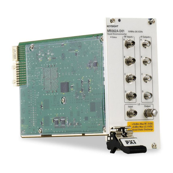
Related Manuals for Keysight M9362AD01


Summary of Contents for Keysight M9362AD01
- Page 1 Keysight Technologies M9362AD01 PXIe Notice: This document contains references to Agilent. Please note that Agilent’s Test and Measurement business has become Keysight Technologies. For more information, go to www.keysight.com. Startup Guide...
- Page 2 EULA. used or copied only in accordance hazard. It calls attention to an Keysight shall be under no obligation with the terms of such license. operating procedure, practice, or the to update, revise or otherwise modify ...
-
Page 3: Table Of Contents
Keysight Support, Services, and Assistance ........ - Page 4 Table of Contents...
- Page 5 M9362AD01...
-
Page 6: M9362Ad01
The scope of this Startup Guide is to detail the processes of receiving and installing the Keysight M9362AD01 PXIe Microwave Quad Downconverter, installing the required software, and verifying basic module operation. If you have any questions after reviewing this information, contact your local Keysight Technologies representative. -
Page 7: Definitions For Specifications
M9362AD01 Introduction Definitions for Specifications Specifications describe the warranted performance of calibrated instruments that have been stored for a minimum of 2 hours within the operating temperature range of 0 to 55°C, unless otherwise stated, and after a 45 minute warm-up period. Data represented in this document are specifications unless otherwise noted. -
Page 8: Step 1: Unpack And Inspect The Module
Refer to “Keysight Support, Services, and Assistance” on page 33. Keep the damaged shipping materials (if any) for inspection by the carrier and an Keysight Technologies representative. To avoid damage when handling a module, do not touch exposed connector pins. http://www.keysight.com/find/tips for information on preventing damage to your Keysight equipment. -
Page 9: Step 2: Verify Shipment Contents
(6.9 in) Available Options Test Set Options The M9362AD01 has three available options, refer to the block diagrams: • Option F26 - 10 MHz to 26.5 GHz Quad Downconverter (Figure 24 on page • Option F40 - 10 MHz to 40 GHz Quad Downconverter (Figure 25 on page •... -
Page 10: Cables
M9362AD01 Cables Cables IF JUMPER CABLES for use with Keysight M9210A PXI-H 10-bit M9362AD01-CA3 High-Speed Digitizing Scope 8120-2066 Cable Assembly, SMA (m) to BNC (m), 190 mm Figure 1 IF Jumper Cable LO INTERCONNECT KIT for use with Keysight M9302A PXI Local... -
Page 11: Step 3: Install The Software
- Utilize a 2x8, 4x4, or 1x4 PXIe system slot link configuration. - Run one of the operating systems listed in System Requirements (above). Remote (for Keysight M9018A chassis use only) Keysight M9021 Cable Interface x8 with one of the following PC Controller interface options:... -
Page 12: Power Up The Controller
PC BEFORE you power down the chassis. If you are using an embedded controller, complete the following steps: 1. Install the embedded controller into the chassis. The Keysight M9306A PXIe Embedded Controller and Keysight M9018A PXIe Chassis are recommended. Refer to the controller and chassis documentation for details. -
Page 13: Step 4: Install The Module
This Module can be used in a chassis with a PXIe and PXI-H hybrid slots. The M9362AD01 can also be installed in any hybrid PXI slot marked with a peripheral slot compatibility image (the letter "H" and a solid circle containing the slot number). - Page 14 8. Install all filler panels after installing the module. Missing filler panels may disrupt necessary air circulation in the chassis. 9. If you are using a PC host, such as the Keysight M9021, connect the Cable Interface in the chassis to the PC host per the instructions that came with the Cable Interface.
-
Page 15: Front Panel Features Option F26
M9362AD01 Front Panel Features Option F26 Front Panel Features Option F26 Figure 4 Front Panel M9362AD01... -
Page 16: M9362Ad01-F26 Connectors
LO Output This APC 3.5 mm female connector outputs a signal (10 MHz to 26.5 GHz) that can be used as the LO Input to an additional M9362AD01 PXIe Microwave Quad Downconverter. Status LED This LED has four possible states: •... -
Page 17: Front Panel Features Option F40
M9362AD01 Front Panel Features Option F40 Front Panel Features Option F40 Figure 5 Front Panel M9362AD01-F40... -
Page 18: M9362Ad01-F40 Connectors
M9362AD01 Front Panel Features Option F40 M9362AD01-F40 Connectors The maximum input to any of the RF Input connectors (A, B, C, or D) must not exceed +10 dBm with 0 VDC offset. The maximum input to the LO Input connector must not exceed +16 dBm with 0 VDC offset. -
Page 19: Front Panel M9362Ad01 Option F50
M9362AD01 Front Panel M9362AD01 Option F50 Front Panel M9362AD01 Option F50 Figure 6 Front Panel M9362AD01-F50... -
Page 20: M9362Ad01-F50 Connectors
M9362AD01 Front Panel M9362AD01 Option F50 M9362AD01-F50 Connectors The maximum input to any of the RF Input connectors (A, B, C, or D) must not exceed +10 dBm with 0 VDC offset. The maximum input to the LO Input connector must not exceed +4 dBm with 0 VDC offset. -
Page 21: General Characteristics
M9362AD01 General Characteristics General Characteristics Table 5 M9362AD01 Typical Characteristics Performance Input and Output Option F26 Option F40 Option F50 Ports Connector Ports Freq Range Connectors Freq Range Connectors Freq Range Connectors RF Port 0.01 to 26.5 GHz 3.5 mm (f) 0.01 to 40 GHz... -
Page 22: Typical Conversion Efficiency Plots
M9362AD01 Typical Conversion Efficiency Plots Typical Conversion Efficiency Plots Set the IF frequency to 10 MHz for conversion efficiency. NOTE Figure 7 F26 Conversion Efficiency Figure 8 F40 Conversion Efficiency... - Page 23 M9362AD01 Typical Conversion Efficiency Plots Figure 9 F50 Conversion Efficiency (Low Band) Figure 10 F50 Conversion Efficiency (High Band)
- Page 24 M9362AD01 Typical Conversion Efficiency Plots Figure 11 F26 IF Bandwidth Figure 12 F40 and F50 IF Bandwid th (Low Band)
- Page 25 M9362AD01 Typical Conversion Efficiency Plots Figure 13 F50 IF Bandwidth (High Band) Figure 14 F26 LO IN to LO OUT Through...
-
Page 26: Operational Procedure
The Operational Procedure can also be verified using two separate PSG sources, one for the RF and a second for the LO. Use a power meter to measure the IF Output. The M9362AD01 performance can be checked against the output power characteristics in the technical... - Page 27 M9362AD01 Operational Procedure Figure 16 Select Measure Figure 17 Source and Attenuator Settings Figure 18 F26 and F50 (Low Band) Frequency Offset...
- Page 28 M9362AD01 Operational Procedure Figure 19 F40 Frequency Offset Figure 20 F50 (High Band) Frequency Offset...
- Page 29 M9362AD01 Operational Procedure Figure 21 F26 and F50 (Low Band) OP Conversion Efficiency Figure 22 F40 OP Conversion Efficiency...
- Page 30 M9362AD01 Operational Procedure Figure 23 F50 (High Band) OP Conversion Efficiency...
-
Page 31: Block Diagrams
M9362AD01 Block Diagrams Block Diagrams Figure 24 M9362AD01 Block Diagram (Option F26) RF IN IF OUT PXIe Slot Interface RF IN IF OUT RF IN IF OUT Interface/ Power Supply RF IN Board IF OUT +/- 9 Volts DC + 15 Volts DC... - Page 32 M9362AD01 Block Diagrams Figure 25 M9362AD01 Block Diagram (Option F40) RF IN IF OUT PXIe Slot Interface RF IN IF OUT RF IN IF OUT Interface/ Power Supply RF IN Board IF OUT +/- 9 Volts DC + 15 Volts DC...
- Page 33 M9362AD01 Block Diagrams Figure 26 M9362AD01 Block Diagram (Option F50) RF IN IF OUT PXIe Slot Interface RF IN IF OUT RF IN IF OUT Interface/ Power Supply RF IN Board IF OUT +/- 9 Volts DC + 15 Volts DC...
-
Page 34: Safety And Information
M9362AD01 Safety and Information Safety and Information Introd uction Review this product and related documentation to familiarize yourself with safety markings and instructions before you operate the instrument. This product has been designed and tested in accordance with accepted industry standards, and has been supplied in a safe condition. -
Page 35: Regulatory Information
M9362AD01 Regulatory Information Regulatory Information This section contains definitions of markings that may be found on or with the product. Instrument Markings South Korean Certification (KC) mark; includes the marking's identifier code in the format shown. R-R-Kst- ZZZZZZZ This symbol indicates separate collection for electrical and electronic equipment, mandated under EU law as of August 13, 2005. - Page 36 • USA: UL std no. 61010-1 Acoustic statement: (European Machinery Directive): • Accoustical noise emission LpA<70 dB Operator position Normal operation mode Per ISO 7779 Declarations of Conformity: To find a current Declaration of Conformity for a specific Keysight product, go to: http://regulations.keysight.com/DoC/search.htm...
-
Page 37: Keysight Support, Services, And Assistance
Should it become necessary to return a module for repair or service, follow the steps below: 1. Review the warranty information shipped with your product. 2. Contact Keysight to obtain a Return Material Authorization (RMA) and return address. If you need assistance finding Keysight contact information go to http://www.keysight.com/find/assist... - Page 38 This information is subject to change without notice. © Keysight Technologies 2010-2017, 2020 Edition 2, March 2020 Supersedes: August 2015 M9499-90001 www.keysight.com...
Need help?
Do you have a question about the M9362AD01 and is the answer not in the manual?
Questions and answers