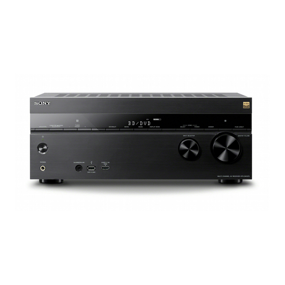
Sony STR-DN1070 Service Manual
Multi channel av receiver
Hide thumbs
Also See for STR-DN1070:
- Operating instructions manual (60 pages) ,
- User manual (169 pages)
Table of Contents
Advertisement
SERVICE MANUAL
Ver. 1.0 2016.03
Note:
Be sure to keep your PC used for service and
checking of this unit always updated with the
latest version of your anti-virus software.
In case a virus affected unit was found during
service, contact your Service Headquarters.
This receiver incorporates Dolby* Digital and Pro
Logic Surround and the DTS** Digital Surround
System.
* Manufactured under license from Dolby Labo-
ratories. Dolby, Pro Logic, Surround EX, and
the double-D symbol are trademarks of Dolby
Laboratories.
** For DTS patents, see http://patents.dts.com.
Manufactured
under
license
from
DTS
Licensing Limited. DTS, DTS-HD, the
Symbol, & DTS and the Symbol together are
registered trademarks, and DTS-HD Master
Audio is a trademark of DTS, Inc. © DTS, Inc.
All Rights Reserved.
This
receiver
incorporates
High-Definition
Multimedia Interface (HDMI™) technology.
The terms HDMI and HDMI High-Definition
Multimedia Interface, and the HDMI Logo are
trademarks or registered trademarks of HDMI
Licensing LLC in the United States and other
countries.
Apple, the Apple logo, AirPlay, iPad, iPhone,
iPod, iPod touch, and Retina are trademarks
of Apple Inc., registered in the U.S. and other
countries.
iPad Air and iPad mini are trademarks of Apple
Inc.
App Store is a service mark of Apple Inc.
"Made for iPod," "Made for iPhone," and "Made
for iPad" mean that an electronic accessory
has been designed to connect specifically to
iPod, iPhone, or iPad, respectively, and has
been certified by the developer to meet Apple
performance standards. Apple is not responsible
for the operation of this device or its compliance
with safety and regulatory standards. Please note
that the use of this accessory with iPod, iPhone, or
iPad may affect wireless performance.
Windows Media is either a registered trademark or
trademark of Microsoft Corporation in the United
States and/or other countries.
This product is protected by certain intellectual
property rights of Microsoft Corporation. Use
or distribution of such technology outside of
this product is prohibited without a license from
Microsoft or an authorized Microsoft subsidiary.
LDAC™ and LDAC logo are trademarks of Sony
Corporation.
MPEG Layer-3 audio coding technology and
patents licensed from Fraunhofer IIS and
Thomson.
"BRAVIA" is a trademark of Sony Corporation.
"PlayStation" is a registered trademark of Sony
Computer Entertainment Inc.
"WALKMAN" and "WALKMAN" logo are
registered trademarks of Sony Corporation.
MICROVAULT is a trademark of Sony Corpora-
tion.
®
®
Wi-Fi
,
Wi-Fi
Protected
Access
,
Wi-Fi
®
®
Alliance
and Wi-Fi CERTIFIED Miracast
are
registered trademarks of Wi-Fi Alliance
®
.
9-890-677-01
Sony Corporation
2016C80-1
©
2016.03
Published by Sony EMCS (Malaysia) PG Tec
STR-DN1070
Wi-Fi CERTIFIED™, WPA™, WPA2™, Wi-Fi
Protected Setup™ and Miracast™ are trademarks
of Wi-Fi Alliance
®
.
DLNA™,
the
DLNA Logo
and
DLNA
CERTIFIED™ are trademarks, service marks, or
certification marks of the Digital Living Network
Alliance.
The BLUETOOTH
®
word mark and logos
are registered trademarks owned by Bluetooth
SIG, Inc. and any use of such marks by Sony
Corporation is under license. Other trademarks
and trade names are those of their respective
owners.
The N Mark is a trademark or registered
trademark of NFC Forum, Inc. in the United
States and in other countries.
Android™ is a trademark of Google Inc.
Google Play™ is a trademark of Google Inc.
Google Cast™ is a trademark of Google Inc.
This product incorporates Spotify software
which is subject to 3rd party licenses found
here*:
https://developer.spotify.com/esdk-third-party-
licenses/
Spotify and Spotify logos are trademarks of the
Spotify Group.*
* This function may not be available in some
countries/regions.
All other trademarks and registered trademarks
are of their respective holders. In this manual, ™
and ® marks are not specified.
Notice on End User License Agreement
(EULA)
For details of the EULA for this product, see
page 54.
For details of the EULA for network services,
please refer to [License agreement] in options
menu on each network service icon.
For details of the GPL, LGPL and other software
licenses, please refer to [Software License
Information] in [System Settings] of the [Setup]
menu on this product.
This product contains software that is subject
to the GNU General Public License ("GPL") or
GNU Lesser General Public License ("LGPL").
These establish that customers have the right to
acquire, modify, and redistribute the source code
of said software in accordance with the terms of
the GPL or the LGPL.
The source code for the software used in this
product is subject to the GPL and LGPL, and is
available on the Web.
To download, please access the following:
URL: http://oss.sony.net/Products/Linux
Please note that Sony cannot answer or respond to
any inquiries regarding the content of this source
code.
SPECIFICATIONS
AUDIO POWER SPECIFICATIONS
POWER OUTPUT AND TOTAL
HARMONIC DISTORTION:
(US models only)
With 6 ohm loads, both channels driven,
from 20 Hz – 20,000 Hz; rated 100 watts per
channel minimum RMS power, with no more
than 0.09% total harmonic distortion from 250
milliwatts to rated output.
Amplifier section
1)
Minimum RMS Output Power
(6 ohms, 20 Hz – 20 kHz, THD 0.09%)
100 W + 100 W
Stereo Mode Output Power
(6 ohms, 1 kHz, THD 1%)
120 W + 120 W
Surround Mode Output Power
2)
(6 ohms, 1 kHz, THD 0.9%)
165 W per channel
Measured under the following conditions:
1)
Area
Power requirements
US, Canadian
120 V AC, 60 Hz
AUS, AEP, UK
230 V AC, 50 Hz
2)
Reference power output for front, center,
surround, surround back and front high
speakers. Depending on the sound field
settings and the source, there may be no
sound output.
Frequency response
Analog
10 Hz – 100 kHz, +0.5/–2 dB (with
sound field and equalizer bypassed)
Input
Analog
Sensitivity: 500 mV/50 kilohms
S/N
: 105 dB (A, 500 mV
)
3)
4)
Digital (Coaxial)
Impedance: 75 ohms
S/N: 100 dB (A, 20 kHz LPF)
Digital (Optical)
S/N: 100 dB (A, 20 kHz LPF)
Output (Analog)
ZONE 2
Voltage: 2 V/1 kilohm
SUBWOOFER
Voltage: 2 V/1 kilohm
Equalizer
Gain levels
±10 dB, 1 dB step
MULTI CHANNEL AV RECEIVER
US Model
Canadian Model
AEP Model
UK Model
Australian Model
INPUT SHORT (with sound field and equalizer
3)
bypassed).
Weighted network, input level.
4)
FM tuner section
Tuning range
US and Canadian models:
87.5 MHz – 108.0 MHz (100 kHz step)
Other models:
87.5 MHz – 108.0 MHz (50 kHz step)
Antenna (aerial)
FM wire antenna (aerial)
Antenna (aerial) terminals
75 ohms, unbalanced
Video section
Inputs/Outputs
Video:
1 Vp-p, 75 ohms
HDMI Video
Resolution
• 480p/60 Hz
• 576p/50 Hz
• 720p/60 Hz, 50 Hz, 24 Hz
• 1080i/60 Hz, 50 Hz
• 1080p/60 Hz, 50 Hz, 30 Hz, 25 Hz, 24 Hz
• 4K/60 Hz, 50 Hz, 30 Hz, 25 Hz, 24 Hz*
* VIDEO 1 supports 4K/60p 4:2:0 8 bit only
Support
HDCP 2.2, HDR, 3D, Deep Color (Deep
Colour), ITU-R BT.2020, ARC
iPhone/iPad/iPod section
BLUETOOTH technology works with iPhone 6s
Plus, iPhone 6s, iPhone 6 Plus, iPhone 6, iPhone
5s, iPhone 5c, iPhone 5, iPhone 4s, iPhone 4, and
iPod touch (5th and 6th generation).
AirPlay works with iPhone, iPad, and iPod touch
with iOS 4.3.3 or later, Mac with OS X Mountain
Lion or later, and PC with iTunes 10.2.2 or later.
You can use "SongPal" app with this receiver via
BLUETOOTH or network connection.
iPhone/iPad/iPod playback via
(USB) port is
not possible.
USB section
(USB) port:
Type A (For connecting USB memory)
Maximum current
1 A
– Continued on next page –
Advertisement
Table of Contents

Subscribe to Our Youtube Channel
Related Manuals for Sony STR-DN1070


Summary of Contents for Sony STR-DN1070
- Page 1 Licensing Limited. DTS, DTS-HD, the from 20 Hz – 20,000 Hz; rated 100 watts per Other models: SIG, Inc. and any use of such marks by Sony Symbol, & DTS and the Symbol together are channel minimum RMS power, with no more 87.5 MHz –...
- Page 2 STR-DN1070 NETWORK section Ethernet LAN 100BASE-TX Wireless LAN Compatible standards: IEEE 802.11 a/b/g/n Security: WPA/WPA2-PSK, WEP Radio frequency: 2.4 GHz, 5 GHz BLUETOOTH section Communication system BLUETOOTH Specifi cation version 4.1 Output BLUETOOTH Specifi cation Power Class 1 Maximum communication range Line of sight approx.
- Page 3 LES DIAGRAMMES SCHÉMATIQUES ET LA LISTE DES PIÈCES SONT CRITIQUES POUR LA SÉCURITÉ DE FONC- TIONNEMENT. NE REMPLACER CES COMPOSANTS QUE PAR DES PIÈCES SONY DONT LES NUMÉROS SONT DON- NÉS DANS CE MANUEL OU DANS LES SUPPLÉMENTS PUBLIÉS PAR SONY.
-
Page 4: Table Of Contents
STR-DN1070 TABLE OF CONTENTS SERVICING NOTES 6-25. Schematic Diagram ..........- MB-1512 Board (Suffi x-11/-21) (14/16) - ....54 6-26. Schematic Diagram DISASSEMBLY - MB-1512 Board (Suffi x-11/-21) (15/16) - ....55 2-1. Disassembly Flow ............6-27. Schematic Diagram 2-2. Case (Stepup) .............. -
Page 5: Servicing Notes
STR-DN1070 SECTION 1 SERVICING NOTES MODEL IDENTIFICATION NOTE OF REPLACING THE WLAN/BT COMBO CARD –BACK PANEL– When the WLAN/BT COMBO CARD is exchanged, the MAC address has been changed. Please print and cut out the following explanations, and return it with the unit that complete the repair. - Page 6 STR-DN1070 MB-1512 BOARD DISCRIMINATION (US and Canadian NOTE OF REPLACING THE IC1911, IC1912, IC1913 models) AND IC1916 ON THE DCDC BOARD In this set, the MB-1512 board has been changed in the midway Replacement of IC1911, IC1912, IC1913 and IC1916 on the DCDC of production.
- Page 7 Be sure to use the buttons on the receiver restore the receiver to the factory default to perform this operation. persists, consult your nearest Sony dealer. settings by the following procedure. This 1. Turn off the receiver. procedure can also be used to initialize 2.
- Page 8 STR-DN1070 NOTE OF REPLACING MB-1512 BOARD OR WLAN/ (Screen 3) BT COMBO CARD Diag When the MB-1512 board or WLAN/BT COMBO card are Category: Bluetooth Device Test replaced, please execute the below service mode. [1] Bluetooth Enable Procedure: [2] Bluetooth Disable...
-
Page 9: Disassembly
STR-DN1070 SECTION 2 DISASSEMBLY • This set can be disassembled in the order shown below. 2-1. DISASSEMBLY FLOW 2-2. CASE (STEPUP) (Page 9) 2-3. WLAN/BT COMBO CARD 2-4. FRONT PANEL SECTION (Page 10) (Page 11) 2-5. MB-1512 BOARD (Page 12) 2-6. -
Page 10: Wlan/Bt Combo Card
STR-DN1070 2-3. WLAN/BT COMBO CARD Note : When the WLAN/BT combo card is replaced, refer to “NOTE OF REPLACING MB-1512 BOARD OR WLAN/ BT COMBO CARD” on page 8. 9 one screw (+BVTP 3 rear side 0 clamp (L35) qa card, WLAN/BT combo... -
Page 11: Front Panel Section
STR-DN1070 2-4. FRONT PANEL SECTION pin, lead heat sink (SQ-N86) cable tie clamp (L35) 4 Cut the 5 Wire is removed cable tie from the clamp (L35). 9 one screw (+BVTP 3 7 CN1391 (4P) HDMI cable 420mm (CN3500) 0 front panel... -
Page 12: Mb-1512 Board
STR-DN1070 2-5. MB-1512 BOARD Note : When the MB-1512 board is replaced, refer to “NOTE OF REPLACING MB-1512 BOARD OR WLAN/BT COMBO CARD” on page 8. ws heat sink assy (HDMI) 8 one screw qf two screws (+BVTP 3 (+BVTP 3... -
Page 13: Back Panel Section
STR-DN1070 2-6. BACK PANEL SECTION clamp (L35) 3 Wire is removed 6 five screws (+BVTP 3 from the clamp (L35). (US, CND) 1 Wire is removed five screws (BV/RING) from the clamp (L35). (EXCEPT US, CND) DCDC board 7 six screws... -
Page 14: Standby Board, Main Board Section
STR-DN1070 2-7. STANDBY BOARD, MAIN BOARD SECTION 3 four screws (+BVTP 3 8 two screws 0 MAIN BOARD 4 STANDBY board (+BVTP 3 section 8 two screws (+BVTP 3 cable tie MAIN board 5 Cut the cable tie rear side... -
Page 15: Test Mode
STR-DN1070 SECTION 3 TEST MODE VACUUM FLUORESCENT DISPLAY TEST MODE SWAP ALL MODE All fl uorescent segments are tested. The signal will be swap to all channels so that all speakers will When this test is activated, all segments light on at the same time, have sound output. - Page 16 STR-DN1070 HISTORY MODE SPECIAL MODE The state that the set is used is memorized. Enable user or service or factory or designer to access test mode. Procedure: Procedure: 1. While pressing [SPEAKERS] and [DISPLAY MODE] buttons 1. Press the [ ] button to turn the power on.
- Page 17 STR-DN1070 SVC SERVICE MODE Items Display Note: The operation in this mode must use a remote commander and TV EVOL DATA SB L,R monitor. DAC MUTE REQ U Setting method of the SVC service mode: DAC MUTE REQ L 1. Connect this unit with TV monitor.
- Page 18 STR-DN1070 2. Menu Tree Service Device Test Service [1] Dia [1] Dia [ ] Lo [ ] Lo [3] Factory Initialize [3] Factory Initialize [4] Network [4] Network [5] Version Up [5] Version Up Video Test [6] System Information [6] System Information...
- Page 19 STR-DN1070 3. Service Mode Menu (Top Menu) 4. Diag (Device Test) This is the top menu of service mode. This screen is used to test devices mounted on the board. Each function is accessed from this screen. Operation: Screen 1: Selects the test category...
- Page 20 STR-DN1070 7. Diag (Wireless LAN Test) 8. Diag (MIC Input Test) This screen performs wireless LAN/Miracast test. This screen performs MIC input test. Note: Not used for the servicing. Screen 1: Selects Wireless LAN Test Category 9. Diag (HDMI Input Test) Operation: This screen performs HDMI input test.
- Page 21 STR-DN1070 12. Log: Error Log (Output of each Log) (Screen 1) This screen displays the contents of each log. Diag Note: Do not refer to the displayed date. Category: Bluetooth Device Test Screen 1: Selects log Operation: Diag [1]/[ ]...
- Page 22 STR-DN1070 13. Factory Initialize (Factory Settings) Contents List: Return all of the unit setting to their factory defaults. Main LSIname Operation: Model 1. Press the [ ] button to turn the power on. Destination 2. While pressing [DISPLAY MODE] button, press and release...
-
Page 23: Fm Tuner Check
STR-DN1070 SECTION 4 FM TUNER CHECK FM AUTO STOP CHECK signal generator Procedure: 1. Turn on the set. 2. Input the following signal from signal generator to FM antenna input directly. Carrier frequency : A = 87.5 MHz, B = 98 MHz, C = 108 MHz... -
Page 24: Troubleshooting
STR-DN1070 SECTION 5 TROUBLESHOOTING... - Page 25 STR-DN1070...
- Page 26 STR-DN1070...
- Page 27 STR-DN1070...
- Page 28 STR-DN1070...
-
Page 29: Diagrams
STR-DN1070 SECTION 6 DIAGRAMS 6-1. BLOCK DIAGRAM – ANALOG AUDIO Section – DIR FUNCTION SELECT IC1414 J1402 (1/2) INL7 AUDIO TV IN R-ch R-ch INR7 >001B ADCL L-IN J1401 (1/2) DIGITAL SECTION R-ch ADCR (Page 30) INL4 AUDIO SA-CD/CD IN... -
Page 30: Block Diagram - Digital Section
STR-DN1070 6-2. BLOCK DIAGRAM – DIGITAL Section – >001B ANALOG AUDIO L-IN ADINL SECTION R-ch ADINR STEREO D/A CONVERTER (Page 29) IC6000 IC6501 WAVE SHAPER XOUT X6000 IC6001 VOUT1 SBL/SBR_OUT DATA4 L/R_IN 24.576MHz VOUT2 R-CH DATAOUT DIR_IN L/R_OUT DATA1 J6000... -
Page 31: Block Diagram - Amp Section
STR-DN1070 6-3. BLOCK DIAGRAM – AMP Section – J1101 POWER AMP PHONES BOOSTER Q1720 Q1700 CURRENT CURRENT Q1722 LIMITER RELAY DETECT DETECT D1700 Q1702, Q1703 DRIVER Q1724 Q1704 Q1705 Q1375 BOOSTER RY1390 Q1725 TB1501 (1/2) Q1701 BOOSTER FRONT A Q1770... -
Page 32: Block Diagram - Memory/Analog Video/Usb Section
STR-DN1070 6-4. BLOCK DIAGRAM – MEMORY/ANALOG VIDEO/USB Section – VIDEO SWITCH J1401 (2/2) IC1232 VIDEO VOUT MONITOR OUT VIDEO >005B 4 SW2 V_SEL_SW2 VIN3 VIDEO 1 IN DIGITAL V_SEL_MUTE VIDEO SECTION MUTE VIN2 3 SAT/CATV IN (Page 30) NAND_RESET J503... -
Page 33: Block Diagram - Digital Video Section (1/2)
STR-DN1070 6-5. BLOCK DIAGRAM – DIGITAL VIDEO Section (1/2) – HDMI TRANSCEIVER HDMI RECEIVER IC3503 IC5004 (2/3) CN4002 DATA2+ P3RX2P P1TX2P P2RX2P DATA2– P3RX2M P1TX2M P2RX2M DATA1+ P2RX1P P3RX1P P1TX1P DATA1– P3RX1M P1TX1M P2RX1M DATA0+ P3RX0P P1TX0P P2RX0P DATA0– P3RX0M... -
Page 34: Block Diagram - Digital Video Section (2/2)
STR-DN1070 6-6. BLOCK DIAGRAM – DIGITAL VIDEO Section (2/2) – HDMI RECEIVER IC5004 (3/3) CN5002 CN5000 DATA2+ DATA2+ P1TX0M P1RX2P DATA2– DATA2– P1RX2M P1TX0P DATA1+ DATA1+ P1TX1M P1RX1P DATA1– DATA1– P1TX1P P1RX1M DATA0+ DATA0+ P1RX0P P1TX2M DATA0– DATA0– OUT B/... -
Page 35: Block Diagram - Display/Power Section
STR-DN1070 6-7. BLOCK DIAGRAM – DISPLAY/POWER Section – VACUUM FLOURESCENT RELAY DRIVER BRIDGEABLE_RY DISPLAY Q920 ND1100 RY920 RECT LED DRIVER PURE_DIRECT_LED (PURE DIRECT) D921 Q1102 D1108 F912 (VCC) AUDIO AMP 51 FL_LAT SECTION F913 LED DRIVER 60 FL_CLK (VCC) FLASH_CLK/PWR_LED... - Page 36 STR-DN1070 THIS NOTE IS COMMON FOR PRINTED WIRING BOARDS AND SCHEMATIC DIAGRAMS. • Circuit Boards Location (In addition to this, the necessary note is printed in each block.) For Printed Wiring Boards. For Schematic Diagrams. DCDC board Note: Note: card, WLAN/BT COMBO •...
-
Page 37: Printed Wiring Board - Mb-1512 Board (Suffi X-11) (Component Side)
STR-DN1070 6-8. PRINTED WIRING BOARD – MB-1512 Board (Suffi x-11) (Component Side) – • See page 36 for Circuit Boards Location. • : Uses unleaded solder. MB-1512 BOARD (COMPONENT SIDE) J6000 COAXIAL SA-CD/CD (ASSIGNABLE) IR REMOTE HDMI J3191 J3190 J503... -
Page 38: Printed Wiring Board - Mb-1512 Board (Suffi X-11) (Conductor Side)
STR-DN1070 6-9. PRINTED WIRING BOARD – MB-1512 Board (Suffi x-11) (Conductor Side) – • See page 36 for Circuit Boards Location. • : Uses unleaded solder. MB-1512 BOARD (CONDUCTOR SIDE) CL3071 CL3075 CL3077 CL3072 CL3510 CL5041 CL5040 CL5039 CL5004 CL5005... -
Page 39: Printed Wiring Board - Mb-1512 Board (Suffi X-21) (Component Side)
STR-DN1070 6-10. PRINTED WIRING BOARD – MB-1512 Board (Suffi x-21) (Component Side) – • See page 36 for Circuit Boards Location. • : Uses unleaded solder. MB-1512 BOARD (COMPONENT SIDE) J6000 COAXIAL SA-CD/CD (ASSIGNABLE) IR REMOTE HDMI J3191 J3190 J503... -
Page 40: Printed Wiring Board - Mb-1512 Board (Suffi X-21) (Conductor Side)
STR-DN1070 6-11. PRINTED WIRING BOARD – MB-1512 Board (Suffi x-21) (Conductor Side) – • See page 36 for Circuit Boards Location. • : Uses unleaded solder. MB-1512 BOARD (CONDUCTOR SIDE) CL3071 CL3075 CL3077 CL3072 CL3510 CL5041 CL5040 CL5039 CL5004 CL5005... - Page 41 STR-DN1070 6-12. SCHEMATIC DIAGRAM – MB-1512 Board (Suffi x-11/-21) (1/16) – • See page 85 for IC Pin Function Descriptions. MB-1512 BOARD (1/16) IC101 (1/15) CXD90028GB-B-E IC101 C101 BD DECODER DDR3_ACH 0.1u AG14 D0DQ0 JL2101 DDRVCCIO1 RDQ0 D0DQ1 IC102 IC103...
-
Page 42: Schematic Diagram - Mb-1512 Board (Suffi X-11/-21) (2/16)
STR-DN1070 6-13. SCHEMATIC DIAGRAM – MB-1512 Board (Suffi x-11/-21) (2/16) – • See page 75 for IC Block Diagrams. • See page 85 for IC Pin Function Descriptions. MB-1512 BOARD (2/16) IC101 (5/15) MTK_3.3V CXD90028GB-B-E IC2001 TH58NVG3S0HTAI0 IC101 MTK_1.2V IC2001... -
Page 43: Schematic Diagram - Mb-1512 Board (Suffi X-11/-21) (3/16)
STR-DN1070 6-14. SCHEMATIC DIAGRAM – MB-1512 Board (Suffi x-11/-21) (3/16) – MB-1512 BOARD (3/16) CN301 C386 100p C387 0.0022u CL303 C318 C319 C317 AC CUT 0.1u C389 470p 0.0022u 0.0022u CL304 POWER-RY CL305 STANDBY +4.5V >006S CL306 IC324 RFDCDC_4.5V S-13A1A00-U5T1U3... -
Page 44: Schematic Diagram - Mb-1512 Board (Suffi X-11/-21) (4/16)
STR-DN1070 6-15. SCHEMATIC DIAGRAM – MB-1512 Board (Suffi x-11/-21) (4/16) – • See page 74 for Waveforms. • See page 85 for IC Pin Function Descriptions. MB-1512 BOARD (4/16) R430 R431 IC101 (8/15) CXD90028GB-B-E IC101 MTKSTB_3.3V CN401 BD DECODER R465 2.2k... - Page 45 STR-DN1070 6-16. SCHEMATIC DIAGRAM – MB-1512 Board (Suffi x-11/-21) (5/16) – • See page 75 for IC Block Diagrams. • See page 85 for IC Pin Function Descriptions. MB-1512 BOARD (5/16) IC503 TPS2553DBVR IC503 USB_RF_3.3V FRONT USB VBUS USB_5.2V C531...
-
Page 46: Schematic Diagram - Mb-1512 Board (Suffi X-11/-21) (6/16)
STR-DN1070 6-17. SCHEMATIC DIAGRAM – MB-1512 Board (Suffi x-11/-21) (6/16) – • See page 85 for IC Pin Function Descriptions. MB-1512 BOARD (6/16) IC101 (13/15) CXD90028GB-B-E MTK_3.3V IC101 R449 >001S C421 MTK_1.2V BD DECODER MB-1512 BOARD IC101 (14/15) 1.2V_DDR POWER/GND... -
Page 47: Schematic Diagram - Mb-1512 Board (Suffi X-11/-21) (7/16)
STR-DN1070 6-18. SCHEMATIC DIAGRAM – MB-1512 Board (Suffi x-11/-21) (7/16) – • See page 75 for IC Block Diagrams. • See page 85 for IC Pin Function Descriptions. >029S MB-1512 BOARD (7/16) MB-1512 BOARD (9/16) (Page 49) >028S MB-1512 BOARD... -
Page 48: Mb-1512 Board (Suffi X-11/-21) (5/16)
STR-DN1070 6-19. SCHEMATIC DIAGRAM – MB-1512 Board (Suffi x-11/-21) (8/16) – • See page 75 for IC Block Diagrams. >024S >027S MB-1512 BOARD MB-1512 BOARD (7/16) (7/16) (Page 47) (Page 47) >025S MB-1512 12 13 11 15 BOARD MB-1512 BOARD (8/16) -
Page 49: Schematic Diagram - Mb-1512 Board (Suffi X-11/-21) (9/16)
STR-DN1070 6-20. SCHEMATIC DIAGRAM – MB-1512 Board (Suffi x-11/-21) (9/16) – • See page 85 for IC Pin Function Descriptions. MB-1512 BOARD (9/16) CN3504 CEC 1 NC 2 C3500 R3518 R3512 CL3500 2.2u IN4_HPD HOT PLUG DET IN4_+5V +5V POWER... -
Page 50: Schematic Diagram - Mb-1512 Board (Suffi X-11/-21) (10/16)
STR-DN1070 6-21. SCHEMATIC DIAGRAM – MB-1512 Board (Suffi x-11/-21) (10/16) – • See page 75 for IC Block Diagrams. >034S >035S MB-1512 BOARD (9/16) MB-1512 BOARD (9/16) (Page 49) (Page 49) MB-1512 BOARD (10/16) >023S MB-1512 BOARD (7/16) IN4_+5V (Page 47) IN3_+5V >036S... -
Page 51: Schematic Diagram - Mb-1512 Board (Suffi X-11/-21) (11/16)
STR-DN1070 6-22. SCHEMATIC DIAGRAM – MB-1512 Board (Suffi x-11/-21) (11/16) – • See page 74 for Waveforms. • See page 75 for IC Block Diagrams. • See page 85 for IC Pin Function Descriptions. >038S MB-1512 BOARD (11/16) >026S MB-1512 BOARD (14/16), (16/16) -
Page 52: Schematic Diagram - Mb-1512 Board (Suffi X-11/-21) (12/16)
STR-DN1070 6-23. SCHEMATIC DIAGRAM – MB-1512 Board (Suffi x-11/-21) (12/16) – • See page 74 for Waveforms. • See page 75 for IC Block Diagrams. J6000 COAXIAL SA-CD/CD (ASSIGNABLE) IN MB-1512 BOARD (12/16) >039S MB-1512 BOARD (11/16) JW6002 JW6000 (Page 51) >043S... -
Page 53: Schematic Diagram - Mb-1512 Board (Suffi X-11/-21) (13/16)
STR-DN1070 6-24. SCHEMATIC DIAGRAM – MB-1512 Board (Suffi x-11/-21) (13/16) – • See page 75 for IC Block Diagrams. >049S MB-1512 BOARD (13/16) MB-1512 BOARD (15/16) (Page 55) R6125 MTK_XPCM_DSD_SEL R6106 IC6020 R6126 FB6013 TC7WH157FK SELECT IC6020 ZONE_L/R C6101 SELECT 0.001u... -
Page 54: 6-25. Schematic Diagram - Mb-1512 Board (Suffi X-11/-21) (14/16)
STR-DN1070 6-25. SCHEMATIC DIAGRAM – MB-1512 Board (Suffi x-11/-21) (14/16) – • See page 75 for IC Block Diagrams. MB-1512 BOARD (14/16) >012S MB-1512 BOARD IC6021 MTK_XPCM_DSD_SEL_IN BA33BC0FP-E2 (4/16) IC6021 (Page 44) +3.3V REG. DADCDC_4.5V >048S C6044 A_+5V MB-1512 BOARD >050S... -
Page 55: Mb-1512 Board (Suffi X-11/-21) (15/16)
STR-DN1070 6-26. SCHEMATIC DIAGRAM – MB-1512 Board (Suffi x-11/-21) (15/16) – • See page 74 for Waveforms. • See page 75 for IC Block Diagrams. • See page 85 for IC Pin Function Descriptions. MB-1512 BOARD (15/16) >040S DA_3.3V MB-1512 BOARD... -
Page 56: 6-27. Schematic Diagram - Mb-1512 Board (Suffi X-11/-21) (16/16)
STR-DN1070 6-27. SCHEMATIC DIAGRAM – MB-1512 Board (Suffi x-11/-21) (16/16) – • See page 75 for IC Block Diagrams. MB-1512 BOARD (16/16) >044S >052S MB-1512 BOARD (12/16) MB-1512 BOARD (14/16) (Page 52) (Page 54) CN8000 CL8036 A_GND CL8047 CL8048 >038S A_GND >053S... -
Page 57: Printed Wiring Board - Main Board (Component Side)
STR-DN1070 6-28. PRINTED WIRING BOARD – MAIN Board (Component Side) – • See page 36 for Circuit Boards Location. • : Uses unleaded solder. >004P MAIN BOARD (COMPONENT SIDE) MB-1512 BOARD (SUFFIX-11) CN8001 SPEAKERS IMPEDANCE USE 6-16 (Page 37) TB1501... -
Page 58: Printed Wiring Board - Main Board (Conductor Side)
STR-DN1070 6-29. PRINTED WIRING BOARD – MAIN Board (Conductor Side) – • See page 36 for Circuit Boards Location. • : Uses unleaded solder. MAIN BOARD (CONDUCTOR SIDE) JL1262 R1218 C1402 CL1339 R1217 JL1261 C1216 C1401 CL1248 CL1200 CL1338 R1214... -
Page 59: Schematic Diagram - Main Board (1/5)
STR-DN1070 6-30. SCHEMATIC DIAGRAM – MAIN Board (1/5) – >058S MAIN MAIN BOARD BOARD (4/5) (1/5) [FL] (Page 62) [FR] [SR] >059S C1548 [SBR] [SBL] R1544 0.1u [SL] MAIN BOARD CL1865 (2/5) C1545 47u 25V R1550 R1850 R1800 R1650 R1750... -
Page 60: Schematic Diagram - Main Board (2/5)
STR-DN1070 6-31. SCHEMATIC DIAGRAM – MAIN Board (2/5) – MAIN BOARD (2/5) R1394 R1396 R1398 FR_OUT FL_OUT R1399 >059S R1395 R1397 Q1321 Q1320 2PD601ART MAIN BOARD PROTECTOR MSB92T1G PROTECTOR (1/5) (Page 59) R1320 C1320 220u 10V R1323 C1323 220u 10V... -
Page 61: Schematic Diagram - Main Board (3/5)
STR-DN1070 6-32. SCHEMATIC DIAGRAM – MAIN Board (3/5) – • See page 75 for IC Block Diagrams. >064S >061S MAIN BOARD (2/5) (Page 60) MAIN BOARD (1/5) (Page 59) 15 16 >054S >070S MAIN BOARD (3/5) MB-1512 BOARD MAIN BOARD... -
Page 62: Schematic Diagram - Main Board (4/5)
STR-DN1070 6-33. SCHEMATIC DIAGRAM – MAIN Board (4/5) – >058S >065S >062S MAIN BOARD MAIN BOARD MAIN BOARD (1/5) (2/5) (1/5) (Page 59) (Page 60) (Page 59) 33 34 MAIN BOARD (4/5) >071S MAIN BOARD (3/5) (Page 61) R1896 R1360... -
Page 63: Schematic Diagram - Main Board (5/5)
STR-DN1070 6-34. SCHEMATIC DIAGRAM – MAIN Board (5/5) – • See page 75 for IC Block Diagrams. MAIN BOARD (5/5) >072S C1202 MAIN BOARD (4/5) C1206 (Page 62) TUNER_GND IC1237 MM1839A33NRE IC1237 C1204 L1200 +3.3V REG. 22nH X1200 12MHz 0.1 0.2 3.3... -
Page 64: Printed Wiring Boards - Panel Section
STR-DN1070 6-35. PRINTED WIRING BOARDS – PANEL Section – • See page 36 for Circuit Boards Location. • : Uses unleaded solder. DISPLAY BOARD MB-1512 BOARD MB-1512 BOARD (SUFFIX-11) (SUFFIX-21) T1100 CN3004 CN3004 (Page 37) (Page 39) >009P >018P CL1123... -
Page 65: Schematic Diagram - Panel Section
STR-DN1070 6-36. SCHEMATIC DIAGRAM – PANEL Section – DISPLAY BOARD CN1102 CL1110 27 FL_GND CL1115 26 FL_5V CL1111 25 FL_GND 24 FL_GND CL1112 23 DGND/ZONE POWER CL1113 22 FL_DATA CL1114 21 AD2 CL1147 20 FL_CLK CL1117 19 FL_BK CL1116 18 FL_STB/LATCH >042S... -
Page 66: Printed Wiring Board - Dcdc Board (Suffi X-11)
STR-DN1070 6-37. PRINTED WIRING BOARD – DCDC Board (Suffi x-11) – • See page 36 for Circuit Boards Location. • : Uses unleaded solder. DCDC BOARD DCDC BOARD (COMPONENT SIDE) (CONDUCTOR SIDE) POWER MB-1512 BOARD TRANSFORMER (SUFFIX-11) STANDBY BOARD (MAIN) -
Page 67: Printed Wiring Board - Dcdc Board (Suffi X-21)
STR-DN1070 6-38. PRINTED WIRING BOARD – DCDC Board (Suffi x-21) – • See page 36 for Circuit Boards Location. • : Uses unleaded solder. DCDC BOARD DCDC BOARD (COMPONENT SIDE) (CONDUCTOR SIDE) POWER MB-1512 BOARD TRANSFORMER (SUFFIX-21) STANDBY BOARD (MAIN) -
Page 68: Schematic Diagram - Dcdc Board (Suffi X-11/-21)
STR-DN1070 6-39. SCHEMATIC DIAGRAM – DCDC Board (Suffi x-11/-21) – DCDC BOARD F940 D1924 5A 250V >076S D5SBA60-F CN1907 CL1961 POWER C1036 0.047u CL1960 TRANSFORMER C1000 C1029 R3 Green 6800u CL1959 0.1u R3 Yellow (MAIN) T901 (Page 70) CN1905 >077S... -
Page 69: Printed Wiring Board - Standby Board
STR-DN1070 6-40. PRINTED WIRING BOARD – STANDBY Board – • See page 36 for Circuit Boards Location. • : Uses unleaded solder. STANDBY BOARD STANDBY BOARD (COMPONENT SIDE) (CONDUCTOR SIDE) T902 POWER TRANSFORMER (SUB) >024P C961 DCDC BOARD C960 (SUFFIX-11) -
Page 70: Schematic Diagram - Standby Board
STR-DN1070 6-41. SCHEMATIC DIAGRAM – STANDBY Board – STANDBY BOARD >073S CN940 MAIN BOARD (4/5) >077S CNP920 PWR RY (Page 62) AC CUT D992 D994 DCDC BOARD R984 F901 RB521SM-30GJT2R CES521 CL904 STBY GND T3.15AL 250V CN1905 (EXCEPT US, CND) -
Page 71: Printed Wiring Board - Frontjack Board
STR-DN1070 6-42. PRINTED WIRING BOARD – FRONTJACK Board – 6-44. PRINTED WIRING BOARD – FRONT HDMI Board – • • • See page 36 for Circuit Boards Location. : Uses unleaded solder. • See page 36 for Circuit Boards Location. -
Page 72: Schematic Diagram - Front Hdmi Board
STR-DN1070 6-45. SCHEMATIC DIAGRAM – FRONT HDMI Board – • See page 75 for IC Block Diagrams. (VIDEO 2 IN) HDMI (CHASSIS) (CHASSIS) CN4002 FRONT HDMI BOARD ET4000 ET4001 FB4001 R4006 VCCA IC4000 VCCB R4008 R4009 TCA9517DGKR CN4000 SCLA SCLB 2.2k... -
Page 73: Printed Wiring Board - Powerkey Board
STR-DN1070 6-46. PRINTED WIRING BOARD – POWERKEY Board – 6-48. PRINTED WIRING BOARD – HP Board – • • • See page 36 for Circuit Boards Location. : Uses unleaded solder. • See page 36 for Circuit Boards Location. : Uses unleaded solder. - Page 74 STR-DN1070 • Waveforms – MB-1512 Board – IC401 5 (2Y) IC6002 qg (LRCKOUT) 3.36 Vp-p 1.0 Vp-p 27.0 MHz 23 s 200 mV/DIV, 10 ns/DIV 500 mV/DIV, 5 s/DIV IC3002 ij (X1) IC6002 qh (DATAOUT) 3.36 Vp-p 4.0 MHz 2.62 Vp-p...
- Page 75 STR-DN1070 • IC Block Diagrams IC4000 TCA9517DGKR (FRONT HDMI BOARD) VCCA 1 SCLA 2 VCCB SDAA 3 SCLB GND 4 V CCB SDAB Pullup Resistor IC1232 NJM41050V (TE2) (MAIN BOARD (5/5)) CLAMP NC_14 VIN1 SSIGV ADVANCED 12 VSAG CORRECTION CLAMP...
- Page 76 STR-DN1070 IC1236 RN5B701-0002 (MAIN BOARD (5/5)) (except US and Canadian models) IISD IISD Digital Signal Processing LOUT Filter LRCK/LOUT Digital Stereo FRF1 1 Mixer Demodulator Decoder BCLK/ROUT FM LNA ROUT RSSI Digital FRF2 2 Calculation Decoder LRCK Image Station BCLK...
- Page 77 STR-DN1070 IC1414 BD34702KS2 (MAIN BOARD (3/5)) Main Sub1 Sub2 SBLIN INR7 SBRIN INL7 SLIN INR8 SRIN INL8 Mode Mode Mode Mode selector selector selector selector SWIN 7.1 ch OUT +32dB ~ -95dB,-INF/0.5dB step FLIN RECR FRIN RECL Volume Volume Volume...
- Page 78 STR-DN1070 IC2001 TH58NVG3S0HTAI0 (MB-1512 BOARD (2/16)) NC_1 48 NC_48 47 NC_47 NC_2 NC_3 46 NC_46 NC_4 45 NC_45 NC_5 44 I/O8 43 I/O7 NC_6 Status register RY / BY 42 I/O6 41 I/O5 Address register Column buffer 40 NC_40 Column decoder...
- Page 79 STR-DN1070 IC3192 TC7SZ32FU, RSONYJ (MB-1512 BOARD (11/16)) IC6019 TC7SZ32FU, RSONYJ (MB-1512 BOARD (14/16)) IN_B 5 VCC IN_A 4 OUT IC3500, IC3502 BU9883FV-WE2 (MB-1512 BOARD (10/16)) VCC1 1 Voltage Detect Logic Low Voltage Logic LEVEL BANK0 SCL1 2 CONTROL (PORT1) Shifter...
- Page 80 STR-DN1070 IC5000 W25Q16DVSSIG (MB-1512 BOARD (7/16)) IC6502 W25Q16DVSSIG (MB-1512 BOARD (15/16)) DO (IO1) Write Control WP (IO2) Logic HOLD (IO3) Status Register High Voltage Generators Page Address Latch / Counter Command and Column Decode Control Logic and 256 Byte Page Buffer...
- Page 81 STR-DN1070 IC6000 AK4458VN (MB-1512 BOARD (14/16)) AOUTR4P Clock MCLK Divider AOUTR4N DATT DSD Filter Soft Mute MODULATOR BICK/DCLK VREFL4 Vref Noise LRCK/DSDL1 VREFH4 Rejection Filter SDTI1/DSDR1 Data Interface SDTI2/DSDL2 AOUTL4N DATT De-emphasis SDTI3/DSDR2/TDMO1 Soft Mute Interpolator AOUTL4P SDTI4/DSDL3/TDMO2 AOUTR3P AOUTR3N...
- Page 82 STR-DN1070 IC6002 LC89075WA-H (MB-1512 BOARD (12/16)) PVDD RXIN1 PGND RXIN2 MCKIN RXIN3 BCKIN Group: A Stereo RXIN4 Group: B LRCKIN Group: C (4x6):4 Group: D RXIN5 DATAIN RXIN6 MPIN1 Group: D (Input) Group: C (Input) RXIN7 MPIN2 Group: A RXIN8...
- Page 83 STR-DN1070 IC6006 CS230002-CZZR (MB-1512 BOARD (13/16)) VD 1 GND 2 OUT_EN CLK_OUT 3 FRACTIONAL-N FILTN FREQUENCY FILTP SYNTHESIZER LOCK 4 M [1:0] OUTPUT TO INPUT 00 = 1 CLOCK RADIO 128 Hz BW DIGITAL PLL 01 = 2 & FRACTIONAL N LOGIC...
- Page 84 STR-DN1070 IC6500 EM638165TSD-6G (MB-1512 BOARD (15/16)) VSS_54 54 VDD_1 DQ15 53 VSSQ_52 52 VDDQ_3 CLOCK DQ14 51 BUFFER DQ13 50 VDDQ_49 49 VSSQ_6 COLUMN DECODER DQ12 48 COLUMN DECODER CONTROL DQ11 47 SIGNAL COMMAND GENERATOR CELL ARRAY VSSQ_46 46 DECODER...
- Page 85 STR-DN1070 • IC Pin Function Descriptions MB-1512 BOARD (1/16), (2/16), (4/16), (5/16), (6/16) IC101 CXD90028GB-B-E (BD DECODER) Pin No. Pin Name Description A1, A2 GPIO14, GPIO12 Not used Two-way I2C data bus terminal Not used USB_DP_P1 Two-way USB serial data (+) bus terminal...
- Page 86 STR-DN1070 Pin No. Pin Name Description C16, C17 Not used Not used Not used C20, C21 Not used Not used Digital audio signal input from the HDMI ARC OUT connector COAXIAL Not used SPDIF Not used NS_XTALI System clock signal input terminal (27 MHz)
- Page 87 STR-DN1070 Pin No. Pin Name Description F9, F10 DGND12_K Ground terminal AVSS33_USB_POP1 Ground terminal Not used Not used F15, F16 DGND12_K Ground terminal AGND33_3 Ground terminal AVDD33_1 Power supply terminal (+3.3V) AGND12_2 Ground terminal AGND33_1 Ground terminal DVCC33_IO_5 Power supply terminal (+3.3V) AVDD33_PLLGP Power supply terminal (+3.3V)
- Page 88 STR-DN1070 Pin No. Pin Name Description DGND12_K Ground terminal K17 to K19 DVCC12_K Power supply terminal (+1.2V) AVSS33_DAC Ground terminal CH0_P_SUB TMDS data (positive) input from the HDMI IN 2 connector CH0_M_SUB TMDS data (negative) input from the HDMI IN 2 connector...
- Page 89 STR-DN1070 Pin No. Pin Name Description Not used Not used R3, R4 Not used Not used DDRVCCIO1 Power supply terminal (+1.5V) DGND12_K Ground terminal DVCC12_K Power supply terminal (+1.2V) R11 to R19 DGND12_K Ground terminal DVCC12_K Power supply terminal (+1.2V)
- Page 90 STR-DN1070 Pin No. Pin Name Description Not used W1, W2 Not used DDRVCCIO1 Power supply terminal (+1.5V) W4, W5 Not used Not used DDRVCCIO1 Power supply terminal (+1.5V) DVCC12_K Power supply terminal (+1.2V) W11, W12 DVCC12_K Power supply terminal (+1.2V)
- Page 91 STR-DN1070 Pin No. Pin Name Description Not used Not used DDRVCCIO1 Power supply terminal (+1.5V) DGND12_K Ground terminal AVDD33_MEMPLL Power supply terminal (+3.3V) DDRVREF_C Reference voltage (+0.75V) input terminal for SD-RAM RDQM2 Data mask signal output to the SD-RAM DGND12_K...
- Page 92 STR-DN1070 Pin No. Pin Name Description AE21 NFREN Read enable signal output to the NAND fl ash AE22 NFCEN2 Digital audio output terminal AE23 NFD0 Two-way data bus with the NAND fl ash AE24 NFWEN Write enable signal output to the NAND fl ash...
- Page 93 STR-DN1070 Pin No. Pin Name Description AH10, RA0, RA7 Address signal output to the SD-RAM AH11 AH13 RCKE Clock enable signal output to the SD-RAM AH14 RDQ2 Two-way data bus with the SD-RAM AH16 RDQS0_ Data strobe signal (negative) output to the SD-RAM...
- Page 94 STR-DN1070 MB-1512 BOARD (1/16) IC102, IC103 NT5CB128M16IP-EK (SD-RAM) Pin No. Pin Name Description VDDQ DQ Power Supply: 1.5V +/-0.075V DQU5 Data Input/output: Bi-directional data bus. DQU7 Data Input/output: Bi-directional data bus. NO_USE Not used NO_USE Not used NO_USE Not used DQU4 Data Input/output: Bi-directional data bus.
- Page 95 STR-DN1070 Pin No. Pin Name Description Input Data Mask: DM is an input mask signal for write data. Input data is masked when DM is sampled HIGH coincident with that input data during a Write access. DM is sampled on both edges of DQS.
- Page 96 STR-DN1070 Pin No. Pin Name Description Command Input: CAS (along with CS) defi ne the command being entered. NO_USE Not used NO_USE Not used NO_USE Not used Clock: CK is differential clock input. All address and control input signals are sampled on the crossing of the negative edge of CK.
- Page 97 STR-DN1070 Pin No. Pin Name Description Bank Address Inputs: BA1 defi ne to which bank an Active, Read, Write or Precharge com- mand is being applied. Bank address also determines if the mode register or extended mode register is to be accessed during a MRS cycle.
- Page 98 STR-DN1070 MB-1512 BOARD (11/16) IC3002 MB9BF128TAPMC-GE2 (SYSTEM CONTROLLER) Pin No. Pin Name Description Power supply pin (+3.3V) RSTN_STATUS DAC RSTN Bit output to MT8506 Not used Not used Not used Not used DAC_DZF DAC Zero Data input detection TEST1/SWOUT_HPD Test pin output for Designer debugging.
- Page 99 STR-DN1070 Pin No. Pin Name Description Regulator stabilization capacity connecting pin Ground terminal Power supply pin (+3.3V) EVOL_DATA Volume data output to BD34702KS2 EVOL_CLK I2C clock signal output to the electrical volume INITX Micom input reset port POWER_KEY Power switch input terminal...
- Page 100 STR-DN1070 Pin No. Pin Name Description DSP_CS Chip select signal output to DSP DSP_MISO Serial data input from the serial fl ash and DSP DSP_MOSI Serial data output to the serial fl ash and DSP DSP_SPICLK Serial data transfer clock signal output to the serial fl ash and DSP...
- Page 101 STR-DN1070 Pin No. Pin Name Description IN6_UCOM_HPD Hotplug Detect output status for HDMIiI Input 6 INSW_UCOM_HPD Hotplug Detect output status for HDMIiI Input Switcher PANA_787_INT Interrupt detection input from Panasonic 787 IN4_UCOM_HPD Hotplug Detect output status for HDMIiI Input 4...
- Page 102 STR-DN1070 MB-1512 BOARD (9/16) IC3503 MN864788 (HDMI TRANSCEIVER) Pin No. Pin Name Description TX0SDA TX port 0 DDC data TX0HPD TX port 0 Hot Plug Detect CH1ASD0 LPCM Audio data (for LF, RF) / IEC60958 Data / DSD Data (Left 3)
- Page 103 STR-DN1070 Pin No. Pin Name Description P2RXCM TMDS RX port 2 clock - P2RXCP TMDS RX port 2 clock + AVDD11RX2 Analog 1.1 V power supply (Rx port2) P2RX0M TMDS RX port 2 CH0 data - P2RX0P TMDS RX port 2 CH0 data + AVDD11RX2 Analog 1.1 V power supply (Rx port2)
- Page 104 STR-DN1070 Pin No. Pin Name Description TX0ARCIN TX port 0 Audio Return Channel Input VDD11 Digital 1.1 V power supply NTEST Test control pin HSCL0 HOST IF 0 host clock NRESET Reset input pin HSDA0 HOST IF 0 host data VDD33 Digital 3.3 V power supply...
- Page 105 STR-DN1070 MB-1512 BOARD (7/16) IC5004 MN864787 (HDMI RECEIVER) Pin No. Pin Name Description TX0SDA TX port 0 DDC data TX0HPD TX port 0 Hot Plug Detect 3 to 8 D0 to D5 Not used VSS_9 Ground terminal Not used VDD11_11 Digital 1.1 V power supply...
- Page 106 STR-DN1070 Pin No. Pin Name Description AVDD11RX3_75 Analog 1.1 V power supply (Rx port3) P3RX1M TMDS RX port 3 CH1 data - P3RX1P TMDS RX port 3 CH1 data + AVDD11RX3_78 Analog 1.1 V power supply (Rx port3) P3RX2M TMDS RX port 3 CH2 data -...
- Page 107 STR-DN1070 Pin No. Pin Name Description P1RX1P TMDS RX port 1 CH1 data + AVDD11RX1_132 Analog 1.1 V power supply (Rx port1) P1RX2M TMDS RX port 1 CH2 data - P1RX2P TMDS RX port 1 CH2 data + VSS_135 Ground AVDD33RX0 Analog 3.3 V power supply (Rx port0)
- Page 108 STR-DN1070 Pin No. Pin Name Description 195 to 200 Q11 to Q6 Not used VSS_201 Ground 202 to 203 Q5 to Q4 Not used VDD33IO_204 Digital 3.3 V power supply 205 to 208 Q3 to Q0 Not used VDD11_209 Digital 1.1 V power supply VDD33_210 Digital 3.3 V power supply...
- Page 109 STR-DN1070 MB-1512 BOARD (15/16) IC6501 ADSST-AVR-3046 (DSP) Pin No. Pin Name Description SDDQM Data mask signal output to the SD-RAM Memory select signal output to the SD-RAM SDCKE Clock enable signal output to the SD-RAM VDD_INT Power supply terminal (+1.2V) (for core)
- Page 110 STR-DN1070 Pin No. Pin Name Description WDTRSTO Watchdog timer reset output terminal Not used Not used VDD_EXT Power supply terminal (+3.3V) (for I/O) SL/SR_OUT Audio signal output to the DSP2 SL/SR_IN Audio signal input terminal BCLK_IN Bit clock signal input terminal...
- Page 111 STR-DN1070 Pin No. Pin Name Description VDD_INT Power supply terminal (+1.2V) (for core) IRQ/GPIO Interrupt request signal output to the main system controller FLAG1 Error signal input terminal FLAG2 Non-LPCM setting signal input terminal MLBCLK Not used FLAG3 Error signal output to the main system controller and DSP2...
-
Page 112: Exploded Views
STR-DN1070 SECTION 7 EXPLODED VIEWS Note: • -XX and -X mean standardized parts, so • Abbreviation The components identifi ed by mark 0 they may have some difference from the : Australian model or dotted line with mark 0 are critical for original one. -
Page 113: Mb-1512 Board
STR-DN1070 7-2. MB-1512 BOARD (EXCEPT US, CND) back panel section (US, CND) #1 (EXCEPT US, CND) front panel section Note 1: When the MB-1512 board is replaced, refer to “NOTE OF REPLACING MB-1512 BOARD OR WLAN/BT COMBO CARD” on page 8. -
Page 114: Front Panel Section
STR-DN1070 7-3. FRONT PANEL SECTION ANT board (ns) NFC-ICON board (ns) HP SUPPORT board (ns) ND1100 EN1100 EN1101 HP board (ns) supplied with EN1100 supplied with EN1101 Note: If wire (fl at type) is replaced, install it after bending it in the same form as that before replacement. -
Page 115: Back Panel Section
STR-DN1070 7-4. BACK PANEL SECTION (EXCEPT US, CND) (EXCEPT US, CND) #1 (US, CND) GND BRACKET board (ns) chassis section Ref. No. Part No. Description Remark Ref. No. Part No. Description Remark * 151 1-500-082-11 CLAMP, SLEEVE FERRITE 0 156... -
Page 116: Chassis Section
STR-DN1070 7-5. CHASSIS SECTION supplied with Q1550, Q1551, Q1600, Q1601, Q1650, Q1651, Q1700, Q1701, Q1750, Q1751, Q1601 Q1800, Q1801, Q1850, Q1851 Q1700 Q1600 Q1701 Q1751 Q1550 Q1750 INSULATION Q1651 Q1551 board (ns) Q1650 Q1801 Q1800 USB INSULATION Q1851 board (ns) -
Page 117: Electrical Parts List
STR-DN1070 SECTION 8 DCDC DISPLAY ELECTRICAL PARTS LIST Note: The components identifi ed by mark 0 • Due to standardization, replacements in • COILS or dotted line with mark 0 are critical for the parts list may be different from the uH: μH... - Page 118 STR-DN1070 DISPLAY FRONTJACK FRONT HDMI MAIN Ref. No. Part No. Description Remark Ref. No. Part No. Description Remark JR114 1-216-296-11 SHORT CHIP A-2083-857-A FRONT HDMI BOARD, COMPLETE (US, CND) A-2124-409-A FRONT HDMI BOARD, COMPLETE JR115 1-216-296-11 SHORT CHIP (EXCEPT US, CND)
- Page 119 STR-DN1070 MAIN Ref. No. Part No. Description Remark Ref. No. Part No. Description Remark D1551 6-502-961-01 DI DA2J10100L IC1412 8-759-274-71 IC NJM4565M (TE2) D1570 6-502-961-01 DI DA2J10100L IC1413 8-759-274-71 IC NJM4565M (TE2) D1571 6-502-961-01 DI DA2J10100L IC1414 6-721-688-01 IC BD34702KS2...
- Page 120 STR-DN1070 MAIN MB-1512 Ref. No. Part No. Description Remark Ref. No. Part No. Description Remark Q1754 6-553-400-01 MSB92T1G < TERMINAL > Q1755 6-553-400-01 MSB92T1G Q1770 6-550-032-01 TRANSISTOR HN4A06J-GRBL (TE85R) TB1501 1-854-007-11 TERMINAL BOARD, SPEAKER 6P (SPEAKERS IMPEDANCE USE 6-16Ω Q1772...
- Page 121 STR-DN1070 MB-1512 Ref. No. Part No. Description Remark Ref. No. Part No. Description Remark < DIODE > FB8000 1-400-862-11 BEAD, FERRITE FB8001 1-400-862-11 BEAD, FERRITE D3000 6-503-759-01 DI RB751V40, 115 FB8002 1-400-862-11 BEAD, FERRITE D3003 6-500-514-01 DIODE BAV70 D3004 6-502-961-01 DI DA2J10100L <...
- Page 122 STR-DN1070 MB-1512 NFC-ICON POWERKEY STANDBY Ref. No. Part No. Description Remark Ref. No. Part No. Description Remark IC6020 8-759-680-48 IC TC7WH157FK NFC-ICON BOARD IC6021 6-705-468-01 IC BA33BC0FP-E2 *************** IC6500 6-720-801-01 IC EM638165TSD-6G IC6501 (Not supplied) IC ADSST-AVR-3046 < CONNECTOR >...
- Page 123 STR-DN1070 Ref. No. Part No. Description Remark MISCELLANEOUS ************** 4-237-065-01 CLAMP (L35) 1-493-092-21 CARD, WLAN/BT COMBO 1-828-240-61 WIRE (FLAT TYPE) (22 CORE) 4-237-065-01 CLAMP (L35) 1-828-412-61 WIRE (FLAT TYPE) (27 CORE) 1-849-318-11 HDMI CABLE420MM 1-828-308-61 WIRE (FLAT TYPE) (7 CORE)
- Page 124 STR-DN1070 REVISION HISTORY Ver. Date Description of Revision 2016.03 How to search for a contact point of signal lines or the like in DIAGRAMS SECTION If a contact point of a BLOCK DIAGRAM, PRINTED WIRING BOARD or SCHEMATIC DIAGRAM is shown in a different page, use the PDF fi...
Need help?
Do you have a question about the STR-DN1070 and is the answer not in the manual?
Questions and answers