
Subscribe to Our Youtube Channel
Related Manuals for hilscher NXHX 4000-JTAG+


Summary of Contents for hilscher NXHX 4000-JTAG+
- Page 1 Device description NXHX 4000-JTAG+ Development board Hilscher Gesellschaft für Systemautomation mbH www.hilscher.com DOC170703HW02EN | Revision 2 | English | 2018-10 | Released | Public...
-
Page 2: Table Of Contents
NXHX Fieldbus interface adapter modules .............. 38 3.3.1 Overview ...................... 38 3.3.2 NXHX-DP...................... 39 3.3.3 NXHX-CO ....................... 39 3.3.4 NXHX-DN...................... 40 NXHX 4000-JTAG+ | Device description © Hilscher 2018 DOC170703HW02EN | Revision 2 | English | 2018-10 | Released | Public... - Page 3 5.19 POWER_SUPPLY_1 ..................... 64 5.20 POWER_SUPPLY_2 ..................... 65 5.21 POWER_SUPPLY_3 ..................... 66 List of figures ......................... 67 List of tables........................... 68 Contacts.......................... 70 NXHX 4000-JTAG+ | Device description © Hilscher 2018 DOC170703HW02EN | Revision 2 | English | 2018-10 | Released | Public...
-
Page 4: Introduction
<Note, where to find further information> 1.1.4 Reference to hardware Hardware Revision Part number NXHX 4000-JTAG+ 7813.100 Table 2: Reference to hardware NXHX 4000-JTAG+ | Device description © Hilscher 2018 DOC170703HW02EN | Revision 2 | English | 2018-10 | Released | Public... -
Page 5: Legal Notes
The manual delivered with the product shall apply. Under no circumstances shall Hilscher Gesellschaft für Systemautomation mbH be liable for direct, indirect, ancillary or subsequent damage, or for any loss of income, which may arise after use of the information contained herein. - Page 6 Introduction 6/70 Liability disclaimer The hardware and/or software was created and tested by Hilscher Gesellschaft für Systemautomation mbH with utmost care and is made available as is. No warranty can be assumed for the performance or flawlessness of the hardware and/or software under all application conditions and scenarios and the work results achieved by the user when using the hardware and/or software.
- Page 7 Additional guarantees Although the hardware and software was developed and tested in-depth with greatest care, Hilscher Gesellschaft für Systemautomation mbH shall not assume any guarantee for the suitability thereof for any purpose that was not confirmed in writing. No guarantee can be granted whereby the...
- Page 8 The customer hereby expressly acknowledges that this document contains trade secrets, information protected by copyright and other patent and ownership privileges as well as any related rights of Hilscher Gesellschaft für Systemautomation mbH. The customer agrees to treat as confidential all of the information made available to customer by Hilscher Gesellschaft für...
-
Page 9: Descriptions And Drawings
– JTAG interface (standard 20-pin connector) – USB 1.1 device connector (“Mini-B” jack) Power connector jack for +24 V · NXHX 4000-JTAG+ | Device description © Hilscher 2018 DOC170703HW02EN | Revision 2 | English | 2018-10 | Released | Public... - Page 10 Power supply unit for +24 V DC voltage supply (1.25 A output) · “Mini-B” USB cable for firmware flashing · NXHX 4000-JTAG+ | Device description © Hilscher 2018 DOC170703HW02EN | Revision 2 | English | 2018-10 | Released | Public...
-
Page 11: Overview
Descriptions and drawings 11/70 Overview 2.2.1 Block diagram Figure 1: NXHX 4000-JTAG+ block diagram NXHX 4000-JTAG+ | Device description © Hilscher 2018 DOC170703HW02EN | Revision 2 | English | 2018-10 | Released | Public... -
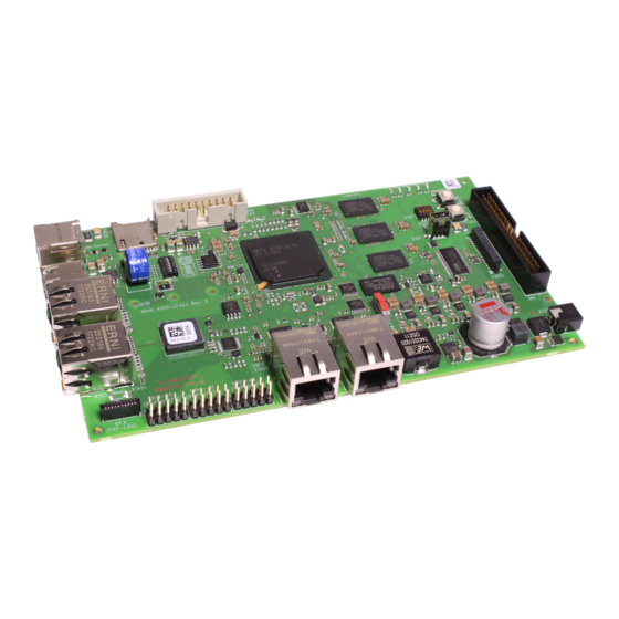
Page 12: Positions Of Interfaces And Operating Elements
Positions of interfaces and operating elements Figure 2: Positions on NXHX 4000-JTAG+ board (view from top) Figure 3: Bottom view NXHX 4000-JTAG+ NXHX 4000-JTAG+ | Device description © Hilscher 2018 DOC170703HW02EN | Revision 2 | English | 2018-10 | Released | Public... -
Page 13: Table 3: Positions On Printed Circuit Board
X1700 PCIe interface (assembly option for mini connector on bottom side of the PCB) Table 3: Positions on printed circuit board NXHX 4000-JTAG+ | Device description © Hilscher 2018 DOC170703HW02EN | Revision 2 | English | 2018-10 | Released | Public... -
Page 14: Operating Elements
USB connection (USB socket X301 of the board) from a development PC (Flasher Tool from Hilscher). For information about how to use the Flasher Tool from Hilscher for the NXHX 4000-JTAG+, see Getting Started document NXHX 4000-JTAG+ Development Board, DOC171004GSxxEN. -
Page 15: Table 4: Functions Of The S300 Dip Switches
(S300-F) GND via 390 Ω Enables alternative boot mode option (not yet supported) Table 4: Functions of the S300 DIP switches NXHX 4000-JTAG+ | Device description © Hilscher 2018 DOC170703HW02EN | Revision 2 | English | 2018-10 | Released | Public... -
Page 16: Table 5: S300 Boot Mode Configuration
3. Secure Digital Input/Output (SDIO): MicroSD Card 4. Real-Time Ethernet Channel 0: DHCP/TFTP server connection (FAQ in preparation) Table 6: S300 boot sequence configuration NXHX 4000-JTAG+ | Device description © Hilscher 2018 DOC170703HW02EN | Revision 2 | English | 2018-10 | Released | Public... -
Page 17: S301 - Dip Switches For User-Defined Inputs
The POR# signal (i.e. the T300 button) resets the full SoC including PLL and debug settings, in contrast to the RST_IN# signal (i.e. the T301 button). NXHX 4000-JTAG+ | Device description © Hilscher 2018 DOC170703HW02EN | Revision 2 | English | 2018-10 | Released | Public... -
Page 18: S1300 - Slide Switch For Sdram/Spm Selection At Host Interface
If this setting is used, the NXHX-FTDI adapter module cannot be used, due to pin sharing restrictions. Table 10: S1300 switch for SDRAM/SPM selection NXHX 4000-JTAG+ | Device description © Hilscher 2018 DOC170703HW02EN | Revision 2 | English | 2018-10 | Released | Public... -
Page 19: Interfaces
Data + Not connected Ground Shield Connected to GND via 1 MΩ and 10nF Table 12: Pin assignments of Mini-B USB connector NXHX 4000-JTAG+ | Device description © Hilscher 2018 DOC170703HW02EN | Revision 2 | English | 2018-10 | Released | Public... -
Page 20: X800 - Usb 2.0 Host Connector ("Type A" Jack)
Transmit/receive data positive channel 4 D4– Transmit/receive data negative channel 4 Bob Smith termination used Table 15: Gigabit Ethernet RJ45 pin assignment NXHX 4000-JTAG+ | Device description © Hilscher 2018 DOC170703HW02EN | Revision 2 | English | 2018-10 | Released | Public... -
Page 21: X1200 - Microsd Card Reader
DAT0 Serial Data 1 DAT1 Card detection Shield Connected to GND via 1 MΩ and 10nF Table 16: Pin assignment X1200 NXHX 4000-JTAG+ | Device description © Hilscher 2018 DOC170703HW02EN | Revision 2 | English | 2018-10 | Released | Public... -
Page 22: X1300 - Host Interface Connector
Not connected Not connected Not connected Not connected +3V3 Not connected Not connected Table 17: Pin assignment of X1300 HIF connector NXHX 4000-JTAG+ | Device description © Hilscher 2018 DOC170703HW02EN | Revision 2 | English | 2018-10 | Released | Public... -
Page 23: X1400/X1401 - Real-Time Ethernet Connectors
Table 18: Ethernet RJ45 pin assignment For a description of the LEDs, see section LEDs on RJ45 Real-Time Ethernet jacks [} page 31] NXHX 4000-JTAG+ | Device description © Hilscher 2018 DOC170703HW02EN | Revision 2 | English | 2018-10 | Released | Public... -
Page 24: X1600 - Connector For Nxhx-Rs232 And Nxhx Fieldbus Adapter Modules
NXHX‑CO for CAN open (part number: 7923.500) · NXHX‑DN for DeviceNet (part number: 7923.510) · NXHX‑CC for CC-Link (part number: 7923.740) · Note: Using an NXHX fieldbus adapter module requires the appropriate fieldbus-specific loadable firmware (LFW) from Hilscher. X1600 Signal MMIO27_UART0_TXD MMIO26_UART0_RXD MMIO29_UART0_RTS# MMIO28_UART0_CTS# +3V3... -
Page 25: Table 20: Pin Assignment X1601
NXHX‑CO for CAN open (part number: 7923.500) · NXHX‑DN for DeviceNet (part number: 7923.510) · NXHX‑CC for CC-Link (part number: 7923.740) · Note: Using an NXHX fieldbus adapter module requires the appropriate fieldbus-specific loadable firmware (LFW) from Hilscher. X1601 Signal MMIO31_UART1_TXD MMIO30_UART1_RXD MMIO33_UART1_RTS# MMIO32_UART1_CTS# +3V3... -
Page 26: X1602 - Connector For Nxhx Fieldbus Adapter Modules
NXHX‑CO for CAN open (part number: 7923.500) NXHX‑DN for DeviceNet (part number: 7923.510) · NXHX‑CC for CC-Link (part number: 7923.740) · Note: Using an NXHX fieldbus adapter module requires the appropriate fieldbus-specific loadable firmware (LFW) from Hilscher. X1602 Signal MMIO44_CAN0_TX MMIO43_CAN0_RX MMIO58_I2S0_SDOUT MMIO57_I2S0_LRCK... -
Page 27: X1603 - Connector Socket For Aifx Detached Fieldbus Interface Modules
27/70 2.4.12 X1603 – Connector socket for AIFX detached fieldbus interface modules Foil connector socket X1603 for connecting Hilscher AIFX detached fieldbus interface modules. For identifying the connector on the board, see position (23) in section Positions of interfaces and operating elements [} page 12]. -
Page 28: X1800 - Interface Connector
MMIO39_GPIO2_7 GPIO2_7 / SPI0_MOSI MMIO40_GPIO2_8 GPIO2_8 / SPI0_MISO MMIO41_GPIO2_9 GPIO2_9 / SPI0_CS0 MMIO42_GPIO2_10 GPIO2_10 +3V3 Table 23: Pin assignments display connector NXHX 4000-JTAG+ | Device description © Hilscher 2018 DOC170703HW02EN | Revision 2 | English | 2018-10 | Released | Public... -
Page 29: X2200 - Connector For +24 V Dc Power Supply
[} page 12]. Socket Number Description 24 V ± 6 V DC GND Ground Table 24: Pin assignment power supply socket NXHX 4000-JTAG+ | Device description © Hilscher 2018 DOC170703HW02EN | Revision 2 | English | 2018-10 | Released | Public... -
Page 30: Leds
COM1 Communication status PHY_COM1_GREEN_A (green) (P1401) (depending on PHY_COM1_RED_A communication protocol) (red) Table 27: COM LEDs on the NXHX 4000-JTAG+ board NXHX 4000-JTAG+ | Device description © Hilscher 2018 DOC170703HW02EN | Revision 2 | English | 2018-10 | Released | Public... -
Page 31: Leds On Rj45 Real-Time Ethernet Jacks
(26) Activity (RX/TX) LED of Real- (yellow) PHY_CH1_YELLOW_A Time Ethernet channel 1 Table 28: RJ45 Ethernet LEDs on NXHX 4000-JTAG+ board NXHX 4000-JTAG+ | Device description © Hilscher 2018 DOC170703HW02EN | Revision 2 | English | 2018-10 | Released | Public... -
Page 32: Leds On Rj45 Gigabit Ethernet Jacks
MMIO03_GPIO0_3 (green) P302 User-definable LED MMIO04_GPIO0_4 (green) P303 User-definable LED MMIO05_GPIO0_5 (green) Table 30: User-definable LEDs on the NXHX 4000-JTAG+ board NXHX 4000-JTAG+ | Device description © Hilscher 2018 DOC170703HW02EN | Revision 2 | English | 2018-10 | Released | Public... -
Page 33: Matrix Label
Figure 4: Matrix label NXHX 4000-JTAG+ In this example, the label shows part number 7813.100, hardware revision 3 and serial number 23457. NXHX 4000-JTAG+ | Device description © Hilscher 2018 DOC170703HW02EN | Revision 2 | English | 2018-10 | Released | Public... -
Page 34: Accessories
Reference potential Request to send Clear to send 9 pin, D-Sub, male 1, 6, 9 n. c. Table 32: RS-232 pin assignment D-Sub NXHX 4000-JTAG+ | Device description © Hilscher 2018 DOC170703HW02EN | Revision 2 | English | 2018-10 | Released | Public... -
Page 35: Nxhx-Ftdi: Serial Dual-Port Memory Via Usb Device At Host Interface
Host interface connector 68 pin, female (at bottom side) Dimensions 65 x 30 mm Order number 7703.050 Table 34: Technical data NXHX-FTDI device NXHX 4000-JTAG+ | Device description © Hilscher 2018 DOC170703HW02EN | Revision 2 | English | 2018-10 | Released | Public... -
Page 36: Table 35: Pinning Host Interface X400 Of Nxhx-Ftdi Device
Pinning of USB interface Name Description VBUS Not connected Data – Data + Not connected Ground Table 36: Pinning of USB interface NXHX 4000-JTAG+ | Device description © Hilscher 2018 DOC170703HW02EN | Revision 2 | English | 2018-10 | Released | Public... - Page 37 JTAG+ board to the downward position: Note: When using the NXHX-FTDI board, the on-board SDRAM cannot be used, due to pin sharing restrictions. NXHX 4000-JTAG+ | Device description © Hilscher 2018 DOC170703HW02EN | Revision 2 | English | 2018-10 | Released | Public...
-
Page 38: Nxhx Fieldbus Interface Adapter Modules
PIO 4 XMAC IO 0 PIO 5 XMAC IO 1 RSTOUT n.c. Table 37: Pins of connector to NXHX Fieldbus adapter NXHX 4000-JTAG+ | Device description © Hilscher 2018 DOC170703HW02EN | Revision 2 | English | 2018-10 | Released | Public... -
Page 39: Nxhx-Dp
CAN H CAN bus high 1, 4, 5, n. c. 6, 8, 9 9 pin, D-Sub, male Table 41: CANopen pin assignment NXHX 4000-JTAG+ | Device description © Hilscher 2018 DOC170703HW02EN | Revision 2 | English | 2018-10 | Released | Public... -
Page 40: Nxhx-Dn
Field ground, internally connected to SLD and PE. Internally connected via 3.3 nF to DG. COMBICON socket, female Table 45: CC-Link pin assignment NXHX 4000-JTAG+ | Device description © Hilscher 2018 DOC170703HW02EN | Revision 2 | English | 2018-10 | Released | Public... -
Page 41: Aifx Detached Fieldbus Interface Devices
41/70 AIFX detached fieldbus interface devices 3.4.1 Overview This section describes the Hilscher AIFX detached fieldbus interface devices that can be connected to the X1603 foil connector socket of the NXHX 4000-JTAG+ board (see position (23) in section Positions of interfaces and operating elements [} page 12]). -
Page 42: Aifx-Co
CAN Low signal DN-L Shield DN_DRAIN CAN High signal DN-H +24 V DeviceNet power supply DN_V+ Table 51: DeviceNet pin assignment NXHX 4000-JTAG+ | Device description © Hilscher 2018 DOC170703HW02EN | Revision 2 | English | 2018-10 | Released | Public... -
Page 43: Aifx-Cc
Internally connected via 3.3 nF to DG. Field ground, internally connected to SLD and PE. Internally connected via 3.3 nF to DG. Table 53: CC-Link pin assignment NXHX 4000-JTAG+ | Device description © Hilscher 2018 DOC170703HW02EN | Revision 2 | English | 2018-10 | Released | Public... -
Page 44: Technical Data Nxhx 4000-Jtag
Dimensions (L x W x D) 170 x 100 x 20 mm Operating temperature 0 … 55 °C Table 54: NXHX 4000-JTAG+ technical data NXHX 4000-JTAG+ | Device description © Hilscher 2018 DOC170703HW02EN | Revision 2 | English | 2018-10 | Released | Public... -
Page 45: Schematic Diagrams
Schematic diagrams 45/70 5 Schematic diagrams Important: Please note that the schematic diagrams are preliminary and may be subject to change. NXHX 4000-JTAG+ | Device description © Hilscher 2018 DOC170703HW02EN | Revision 2 | English | 2018-10 | Released | Public... -
Page 46: Jtag_Reset_Rdy_Run
Schematic diagrams 46/70 JTAG_RESET_RDY_RUN Figure 7: "JTAG_RESET_RDY_RUN" schematic diagram NXHX 4000-JTAG+ | Device description © Hilscher 2018 DOC170703HW02EN | Revision 2 | English | 2018-10 | Released | Public... -
Page 47: Debugging
Schematic diagrams 47/70 Debugging Figure 8: “Debugging” schematic diagram NXHX 4000-JTAG+ | Device description © Hilscher 2018 DOC170703HW02EN | Revision 2 | English | 2018-10 | Released | Public... -
Page 48: Ddr3_Netx
Schematic diagrams 48/70 DDR3_NETX Figure 9: “DDR3_NETX” schematic diagram NXHX 4000-JTAG+ | Device description © Hilscher 2018 DOC170703HW02EN | Revision 2 | English | 2018-10 | Released | Public... -
Page 49: Ddr3_Chip1
Schematic diagrams 49/70 DDR3_CHIP1 Figure 10: "DDR3_CHIP1" schematic diagram NXHX 4000-JTAG+ | Device description © Hilscher 2018 DOC170703HW02EN | Revision 2 | English | 2018-10 | Released | Public... -
Page 50: Ddr3_Chip2
Schematic diagrams 50/70 DDR3_CHIP2 Figure 11: "DDR3_CHIP2" schematic diagram NXHX 4000-JTAG+ | Device description © Hilscher 2018 DOC170703HW02EN | Revision 2 | English | 2018-10 | Released | Public... -
Page 51: Ddr3_Chipecc
Schematic diagrams 51/70 DDR3_CHIPECC Figure 12: "DDR3_CHIPECC" schematic diagram NXHX 4000-JTAG+ | Device description © Hilscher 2018 DOC170703HW02EN | Revision 2 | English | 2018-10 | Released | Public... -
Page 52: Usb 2.0
Schematic diagrams 52/70 USB 2.0 Figure 13: “USB 2.0” schematic diagram NXHX 4000-JTAG+ | Device description © Hilscher 2018 DOC170703HW02EN | Revision 2 | English | 2018-10 | Released | Public... -
Page 53: Rgmii_Netx_Thermal
Schematic diagrams 53/70 RGMII_NETX_THERMAL Figure 14: “RGMII_NETX_THERMAL” schematic diagram NXHX 4000-JTAG+ | Device description © Hilscher 2018 DOC170703HW02EN | Revision 2 | English | 2018-10 | Released | Public... -
Page 54: Rgmii_Phy1
Schematic diagrams 54/70 RGMII_PHY1 Figure 15: “RGMII_PHY1” schematic diagram NXHX 4000-JTAG+ | Device description © Hilscher 2018 DOC170703HW02EN | Revision 2 | English | 2018-10 | Released | Public... -
Page 55: Rgmii_Phy2
Schematic diagrams 55/70 5.10 RGMII_PHY2 Figure 16: “RGMII_PHY2” schematic diagram NXHX 4000-JTAG+ | Device description © Hilscher 2018 DOC170703HW02EN | Revision 2 | English | 2018-10 | Released | Public... -
Page 56: I2C_Rtc_Microsd
Schematic diagrams 56/70 5.11 I2C_RTC_MICROSD Figure 17: "I2C_RTC_MICROSD" schematic diagram NXHX 4000-JTAG+ | Device description © Hilscher 2018 DOC170703HW02EN | Revision 2 | English | 2018-10 | Released | Public... -
Page 57: Sdram_Spm
Schematic diagrams 57/70 5.12 SDRAM_SPM Figure 18: "SDRAM_SPM" schematic diagram NXHX 4000-JTAG+ | Device description © Hilscher 2018 DOC170703HW02EN | Revision 2 | English | 2018-10 | Released | Public... -
Page 58: Rte
Schematic diagrams 58/70 5.13 RTE Figure 19: “RTE” schematic diagram NXHX 4000-JTAG+ | Device description © Hilscher 2018 DOC170703HW02EN | Revision 2 | English | 2018-10 | Released | Public... -
Page 59: Lvds
Schematic diagrams 59/70 5.14 LVDS Figure 20: “LVDS” schematic diagram NXHX 4000-JTAG+ | Device description © Hilscher 2018 DOC170703HW02EN | Revision 2 | English | 2018-10 | Released | Public... -
Page 60: Mmio_Fiberoptic
Schematic diagrams 60/70 5.15 MMIO_FIBEROPTIC Figure 21: “MMIO_FIBEROPTIC” schematic diagram NXHX 4000-JTAG+ | Device description © Hilscher 2018 DOC170703HW02EN | Revision 2 | English | 2018-10 | Released | Public... -
Page 61: Minipciexpress
Schematic diagrams 61/70 5.16 MINIPCIEXPRESS Figure 22: “MINIPCIEXPRESS” schematic diagram NXHX 4000-JTAG+ | Device description © Hilscher 2018 DOC170703HW02EN | Revision 2 | English | 2018-10 | Released | Public... -
Page 62: Rgb
Schematic diagrams 62/70 5.17 RGB Figure 23: “RGB” schematic diagram NXHX 4000-JTAG+ | Device description © Hilscher 2018 DOC170703HW02EN | Revision 2 | English | 2018-10 | Released | Public... -
Page 63: Power
Schematic diagrams 63/70 5.18 POWER Figure 24: “POWER” schematic diagram NXHX 4000-JTAG+ | Device description © Hilscher 2018 DOC170703HW02EN | Revision 2 | English | 2018-10 | Released | Public... -
Page 64: Power_Supply_1
Schematic diagrams 64/70 5.19 POWER_SUPPLY_1 Figure 25: “POWER_SUPPLY_1” schematic diagram NXHX 4000-JTAG+ | Device description © Hilscher 2018 DOC170703HW02EN | Revision 2 | English | 2018-10 | Released | Public... -
Page 65: Power_Supply_2
Schematic diagrams 65/70 5.20 POWER_SUPPLY_2 Figure 26: “POWER_SUPPLY_2” schematic diagram NXHX 4000-JTAG+ | Device description © Hilscher 2018 DOC170703HW02EN | Revision 2 | English | 2018-10 | Released | Public... -
Page 66: Power_Supply_3
Schematic diagrams 66/70 5.21 POWER_SUPPLY_3 Figure 27: “POWER_SUPPLY_3” schematic diagram NXHX 4000-JTAG+ | Device description © Hilscher 2018 DOC170703HW02EN | Revision 2 | English | 2018-10 | Released | Public... -
Page 67: List Of Figures
Figure 25: “POWER_SUPPLY_1” schematic diagram ............64 Figure 26: “POWER_SUPPLY_2” schematic diagram ............65 Figure 27: “POWER_SUPPLY_3” schematic diagram ............66 NXHX 4000-JTAG+ | Device description © Hilscher 2018 DOC170703HW02EN | Revision 2 | English | 2018-10 | Released | Public... - Page 68 Table 38: NXHX-DP technical data ..................Table 39: PROFIBUS pin assignment on NXHX-DP .............. Table 40: NXHX-CO technical data ..................NXHX 4000-JTAG+ | Device description © Hilscher 2018 DOC170703HW02EN | Revision 2 | English | 2018-10 | Released | Public...
- Page 69 DeviceNet pin assignment ..................Table 52: AIFX-CC technical data ..................Table 53: CC-Link pin assignment..................Table 54: NXHX 4000-JTAG+ technical data ................. NXHX 4000-JTAG+ | Device description © Hilscher 2018 DOC170703HW02EN | Revision 2 | English | 2018-10 | Released | Public...
-
Page 70: Contacts
Fax: +49 (0) 6190 9907-50 E-mail: info@hilscher.com Support Phone: +49 (0) 6190 9907-99 E-mail: de.support@hilscher.com SUBSIDIARIES China Japan Hilscher Systemautomation (Shanghai) Co. Ltd. Hilscher Japan KK 200010 Shanghai Tokyo, 160-0022 Phone: +86 (0) 21-6355-5161 Phone: +81 (0) 3-5362-0521 E-mail: info@hilscher.cn E-mail: info@hilscher.jp...
Need help?
Do you have a question about the NXHX 4000-JTAG+ and is the answer not in the manual?
Questions and answers