Roland V-Synth XT Service Notes
Hide thumbs
Also See for V-Synth XT:
- Owner's manual (213 pages) ,
- Supplementary manual (22 pages) ,
- Install manual (1 page)
Table of Contents
Advertisement
Quick Links
MAY.2005
TABLE OF CONTENTS
CAUTIONARY NOTES ................................................... 2
SPECIFICATIONS............................................................. 2
LOCATION OF CONTROLS .......................................... 4
LOCATION OF CONTROLS PARTS LIST ................... 4
LOCATION OF CONTROLS .......................................... 6
LOCATION OF CONTROLS PARTS LIST .................. 7
EXPLODED VIEW 1 ......................................................... 8
EXPLODED VIEW PARTS LIST 1 ................................. 9
EXPLODED VIEW 2 ....................................................... 10
EXPLODED VIEW PARTS LIST 2 ................................ 10
EXPLODED VIEW 3 ....................................................... 12
EXPLODED VIEW PARTS LIST 3 ............................... 13
EXPLODED VIEW 4 ....................................................... 14
EXPLODED VIEW PARTS LIST 4 ............................... 15
WIRING DIAGRAM....................................................... 16
PARTS LIST...................................................................... 18
DRIVER INSTALLATION AND SETTINGS .............. 25
CHECKING THE VERSION NUMBER....................... 25
USERS DATA SAVE AND LOAD................................ 25
FACTORY RESET INSTRUCTIONS ............................ 26
UPDATING THE SYSTEM ............................................ 27
TEST MODE..................................................................... 27
Copyright © 2005 ROLAND CORPORATION
All rights reserved. No part of this publication may be reproduced in any form without the written permission
of ROLAND CORPORATION.
WRITING THE SERIAL ID............................................ 33
BLOCK DIAGRAM......................................................... 36
CIRCUIT BOARD (MAIN) ............................................ 38
CIRCUIT BOARD (MAIN) ............................................ 39
CIRCUIT DIAGRAM (MAIN 1/5) .............................. 40
CIRCUIT DIAGRAM (MAIN 2/5) .............................. 42
CIRCUIT DIAGRAM (MAIN 3/5) .............................. 44
CIRCUIT DIAGRAM (MAIN 4/5) .............................. 46
CIRCUIT DIAGRAM (MAIN 5/5) .............................. 48
CIRCUIT BOARD (PANEL) .......................................... 50
CIRCUIT BOARD (PANEL) .......................................... 52
CIRCUIT DIAGRAM (PANEL 1/1) ............................ 54
CIRCUIT DIAGRAM (ENCODER 1/1) ...................... 56
CIRCUIT DIAGRAM (INLET 1/1)............................... 57
CIRCUIT BOARD (JACK).............................................. 58
CIRCUIT BOARD (JACK).............................................. 60
CIRCUIT DIAGRAM (JACK 1/2) ................................ 62
CIRCUIT DIAGRAM (JACK 2/2) ................................ 64
CIRCUIT DIAGRAM (MIC 1/1)................................... 66
CIRCUIT DIAGRAM (INVERTER 1/1) ..................... 68
CIRCUIT DIAGRAM (CARD 1/1) .............................. 70
ERROR MESSAGES ....................................................... 72
17058326E0
SERVICE NOTES
Issued by RJA
Printed in Japan (0450) (AS)
V-SynthXT
Advertisement
Table of Contents

Subscribe to Our Youtube Channel
Related Manuals for Roland V-Synth XT


Summary of Contents for Roland V-Synth XT
-
Page 1: Table Of Contents
CIRCUIT DIAGRAM (CARD 1/1) ......70 TEST MODE..............27 ERROR MESSAGES ............72 Copyright © 2005 ROLAND CORPORATION All rights reserved. No part of this publication may be reproduced in any form without the written permission of ROLAND CORPORATION. 17058326E0... -
Page 2: Cautionary Notes
MAY.2005 CAUTIONARY NOTES SPECIFICATIONS V-Synth XT: Synthesizer Sound Module User data status Sound Generator Configuration User data status after each of the following processes is described below. Oscillator (envelope x 4 + LFO x 1) x 2 Whenever carrying out procedures that involve deleting or erasing user data,... -
Page 3: Power Supply
V-SynthXT Signal Processing Accessories Internal Processing V-Synth XT Owner’s Manual (#72909756) (JAPANESE (OPTION) #72909389) Sound generating section: 32 bits (floating point) V-Card Owner’s Manual (#72909756) (JAPANESE (OPTION) #72909389) Effects section: 24 bits (fixed point) Sound List (#72909756) (JAPANESE (OPTION) #72909389) -
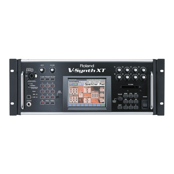
Page 4: Location Of Controls
MAY.2005 V-SynthXT LOCATION OF CONTROLS [FRONT] fig.front-panel.eps LOCATION OF CONTROLS PARTS LIST [FRONT] PART CODE PART NAME DESCRIPTION Q’TY PART CODE PART NAME DESCRIPTION Q’TY 03562256 ROTARY POTENTIOMETER EVUF2AE20B14 03567023 SLIDE SWITCH SSSF12A000 72909412 LCD ASSY 03785112 XLR CONNECTOR NCJ6FI-H 03565234 J R-KNOB SF-ELA BLK/SLV... -
Page 5: Location Of Controls
MAY.2005 V-SynthXT LOCATION OF CONTROLS fig.rear-panel.eps LOCATION OF CONTROLS PARTS LIST REAR PART CODE PART NAME DESCRIPTION Q’TY 02675701 AC INLET ASSY WIRING W3(AC INLET+GND) 03235789 OPTICAL CONNECTOR GP1FA513TZ 03237556 OPTICAL CONNECTOR GP1FA513RZ 03231812 RCA(PIN) YKC21-4173 13429274 MIDI SOCKET YKF51-5041 00120434 JACK YKB21-5227... -
Page 6: Exploded View 1
MAY.2005 EXPLODED VIEW 1 fig.V-SynthXT-Bunkai-e.eps Refer to FigA... -
Page 7: Exploded View Parts List 1
V-SynthXT EXPLODED VIEW PARTS LIST 1 PART CODE PART NAME DESCRIPTION Q’TY 03565234 J R-KNOB SF-ELA BLK/SLV 03903489 DISPLAY ESCT DGM 01786012 SEESAW SWITCH JW-M11RKK 03565789 M R-KNOB LF-ELA BLK 01786045 SW HOLDER AT-217K 03897534 HANDLE 03897578 PANEL PLATE 03897523 FRONT PANEL 03897545 KEY ESCT A... -
Page 8: Exploded View 2
MAY.2005 V-SynthXT EXPLODED VIEW 2 fig.V-SynthXT-BunkaiBetsu-e.eps EXPLODED VIEW PARTS LIST 2 PART CODE PART NAME DESCRIPTION Q’TY PART CODE PART NAME DESCRIPTION Q’TY 03897601 RACK ANGLE CENTER 72909467 JACK BOARD ASSY 03897612 RACK ANGLE L 72909567 INLET BOARD ASSY 03897623 RACK ANGLE R 02894367 INSULATING COVER... -
Page 9: Exploded View 3
MAY.2005 EXPLODED VIEW 3 fig.V-SynthXT-Heimen-e.eps View3 View2 View1... -
Page 10: Exploded View Parts List 3
V-SynthXT EXPLODED VIEW PARTS LIST 3 PART CODE PART NAME DESCRIPTION Q’TY 40011312 SCREW 3X8 BINDING TAPTITE P BZC 40011490 SCREW M3X6 PAN MACHINE W/SW BZC VIEW 3 PART CODE PART NAME DESCRIPTION Q’TY 40011478 SCREW M4X10 PAN SEMS FE ZC 40011090 SCREW 3X6 BINDING TAPTITE B BZC... -
Page 11: Exploded View 4
MAY.2005 EXPLODED VIEW 4 fig.V-SynthXT-HeimenBetsu-e.ep Front Rear View4 View5 BOTTOM... -
Page 12: Exploded View Parts List 4
V-SynthXT EXPLODED VIEW PARTS LIST 4 FRONT PART CODE PART NAME DESCRIPTION Q’TY 40017934 SCREW M3X6 PAN MACHINE W/SW+PW(L) FE ZC REAR PART CODE PART NAME DESCRIPTION Q’TY 40011312 SCREW 3X8 BINDING TAPTITE P BZC 40011490 SCREW M3X6 PAN MACHINE W/SW BZC 40011090 SCREW 3X6 BINDING TAPTITE B BZC... -
Page 13: Wiring Diagram
MAY.2005 V-SynthXT WIRING DIAGRAM fig.wire.eps (1.0p-FPC) L=50 (03897890) BOARD-Connection Diagram (03565345) (03018734) (USB) (EEPROM) L=220 L=60 (0.5p-FPC) (1.0p-FPC) Shield (Digital) (PC-CARD) (Digital) (03018745) L=60 (72909434) MAIN BOARD ASSY (Analog) (1.0p-FPC) (Analog) (72909489) (72909467) CARD BOARD ASSY JACK BOARD ASSY CN12 (H-UDI) (Analog) (Power) -
Page 14: Parts List
MAY.2005 PARTS LIST fig.part1e Due to one or more of the following reasons, SAFETY PRECAUTIONS: parts with parts code ******** cannot be supplied as service parts. The parts marked have safety-related characteristics. Use only listed parts for replacement. • Part supplied only as a component in a complete assembly •... - Page 15 V-SynthXT SPEAKER, BUZZER 03900712 TWEETER PKM13EPYH4002-B0 SPEAKER SP1 on IVB PCB ASSY 72909423 MAIN BOARD ASSY 72909478 INVERTER BOARD ASSY 72909489 CARD BOARD ASSY NOTE: ‘CARD BOARD ASSY’ includes the following parts. 03562156 PC CARD ESCUTCHEON 03897589 PC CARD HOLDER 40011312 SCREW 3X8 BINDING TAPTITE P BZC...
- Page 16 MAY.2005 02456756 TC74VHCT04AFT(EL) IC (CMOS) IC20 on IVB,IC10 on JKB 15289151 NJM2904M-TE3 IC (OP AMP) IC21 on IVB 15289402 TA78L05F(TE12L) IC (REGULATOR) IC15 on IVB 02563467 NJM2374AM-TE1 IC (SWITCHING REGULATOR) IC16 on IVB 03343334 TC75S51FU(TE85L) IC (OP LINEAR) IC23 on MCB 03675801 NE5532AP IC (BIPOLAR OP)
- Page 17 V-SynthXT RESISTOR 00567178 RPC05T 152 J MTL.FILM RESISTOR R166,R205,R169 on MAB ,R98 on JKB 00567189 RPC05T 182 J MTL.FILM RESISTOR R43 on MAB 00567190 RPC05T 222 J MTL.FILM RESISTOR R110,R192 on MAB 00567212 RPC05T 332 J MTL.FILM RESISTOR R177 on MAB ,R206,R200,R49,R16,R32,R37 on JKB,R140,R134 on MCB 00567245 RPC05T 472 J...
- Page 18 MAY.2005 RESISTOR 15419701 RR1220P-103-D 10K OHM (CHIP) MTL.FILM RESISTOR R30,R35,R45,R195,R196,R199,R202,R205,R1 5,R201 on JKB,R103,R106,R114,R117 on 00567267 RPC05T 682 J MTL.FILM RESISTOR R136,R146 on MCB 00567001 RPC05T 750 J MTL.FILM RESISTOR R86,R102 on JKB 00567312 RPC05T 183 J MTL.FILM RESISTOR R100 on JKB 00567345 RPC05T 333 J MTL.FILM RESISTOR...
- Page 19 V-SynthXT CAPACITOR 01674190 ECJ1VC1H150J CERAMIC CAPACITOR C177,C231 on MAB,C138 on IVB,C32,C42 on JKB,C90,C83 on MCB,C999 on CDB 02014856 ECHU1C472JX5 POLYEST. CAPACITOR C255 on MAB 02783412 6SVP150 OS-CON CHEMICAL CAPACITOR C56,C175 on MAB 02900512 EEE1CA100SR CHEMICAL CAPACITOR C65,C155,C196,C213,C198,C182,C132,C130, C137,C133 on MAB 02904412 6SVP47M OS-CON CHEMICAL CAPACITOR...
- Page 20 MAY.2005 CONNECTOR 02012056 CONNECTOR 28FMN-BTK-A CONNECTOR CN25 on IVB 02566489 SM02(8.0)B-BHS-TB CONNECTOR to LCD ASSY ,CN21 on IVB 02782467 10FMN-BTK CONNECTOR CN23 on IVB ,CN3 on ECB 01345567 PS-10PE-D4T1-PN1 CONNECTOR CN26 on IVB 02124789 52043-0410 1MM PITCH FOR CONNECTOR to LCD ASSY ,CN22 on IVB 13369592 B7B-XH-A(7P) JST CONNECTOR...
-
Page 21: Driver Installation And Settings
A pulldown menu will appear. Synth XT. fig.version-1.eps (XP recommended.) PC in which the USB-MIDI driver for V-Synth XT is installed when the test mode is executed is necessary. DRIVER CD-ROM (#03897734) Please see manual P.138 about the method of installing the driver. -
Page 22: Factory Reset Instructions
MAY.2005 Detach the USB cable from V-Synth XT after operating PC referring to Press <EXIT> button to back to the primaly screen. “Closing the USB Storage Screen” and “Canceling the USB Connection” 3. Verifycation of the backup data. (P.140) of the manual after coping the files. -
Page 23: Updating The System
Please exchange the main board Assy when you still can not update correctly. Turn off and on to reboot the V-Synth XT and verifying the new version program, then check the version number if you need. TEST MODE If the main board aseembly is replaced when the V-Synth/XT serviced at a service station, you must write the Serial ID number into the main board assembly before executing the test mode. - Page 24 MAY.2005 Button operations The sequence note pattern is repeated for the test. (MAIN-OUT, PHONES) Listen to the sound, and verify that there is no noise or other problem with the sound. Entering Test mode Perform the impact test. Lift the body of front side to a higher position (about 1-inch) and drop it, when While holding down the two buttons [PREVIEW] [BANK-], turn on the power.
- Page 25 V-SynthXT 3: Memory Test fig.13-6.eps fig.13-4.eps Set [VOLUME] and [INPUT] knobs to the maximum setting. First check the MAIN OUT output. NOR FLASH, SDRAM, EEPROM, and ESP will be checked automatically. Connect the Oscilloscope. If all tests are OK, you will automatically proceed to the next test item. Press [ The MAIN OUT-L will output a triangle wave, and the MAIN OUT-R will Problem...
- Page 26 MAY.2005 sine wave, at sampling rate of 96kHz. fig.13-8.eps Press [ ] to proceed to the next step. Connect the external digital audio input device (MA-10D, etc.), to OUT A (optical) jack. Check the sound or wave shape of connected external device. The digital audio data from OUT A;...
- Page 27 Using the touch pen, touch the center of “+” symbol enclosed the box. When the touch has been detected, the box will move to the next point. Verify that the V-Synth XT produces a beep when you touch the screen. When you have touched all four points on the screen, calibration willbe performed.
- Page 28 DIRECT OUT. Check card slot operation. Insert a PC card into the PC card slot. Use a PC card formatted by the V-Synth XT. Press [ ] Write/Read tests will be performed. If they were successful, the display will indicate “OK”.
-
Page 29: Writing The Serial Id
When the USB Storage connection is normally recognized, it is displayed on the screen, “USB Connect: OK”. 14: USB MIDI/Audio Test Then disconnect the USB cable from V-Synth XT, it is displayed on the screen, “USB Disconnect: OK”. Checking the USB MIDI mode connection. - Page 30 MAY.2005 fig.gidstamp.eps fig.gidstamps.eps If the model ID has registered, select the “V-Synth XT” in the item of [Select Input the serial ID of the product (seven characters) to [SERIAL No] field of Model] field. [Input ID] frame, Please advance to procedure 7.
- Page 31 V-SynthXT...
-
Page 32: Block Diagram
MAY.2005 V-SynthXT BLOCK DIAGRAM fig.block.eps IC5,8,9,10 (MainMemory) CARD IC65 3.3V 1.55V IC39 IC42 DC/DC SDRAM SDRAM BOARD BLOCK DIAGRAM DC/DC 5Vto1.55V NAND PC-CARD 5Vto3.3V 256Mbit 256Mbit 133MHz IC44 I/F-Logic FLASH FLASH CORE (BootSystem) Ctrl (FileStorage) &Buffer POWER 64Mbit Logic 256Mbit (x6) IC66 EEPROM... -
Page 33: Circuit Board (Main)
MAY.2005 CIRCUIT BOARD (MAIN) fig.b-main1.eps View from components side... -
Page 34: Circuit Board (Main)
V-SynthXT CIRCUIT BOARD (MAIN) fig.b-main2.eps View from foil side... -
Page 35: Circuit Diagram (Main 1/5)
MAY.2005 V-SynthXT CIRCUIT DIAGRAM (MAIN 1/5) fig.c-main1.eps SDRAM (256Mbitx4) 33.25MHz RA44 LED1 RA16 IC15 RA17 66.5MHz RA31 RA18 133MHz RA10 IC17 RA36 RA32 R214 RA33 RA22 R248 IC16 RA34 RA11 RA35 RA23 RA12 IC11 RA24 RA27 RA42 HD6417297BP267 IC10 IC18 RA25 RA28 RA41... -
Page 36: Circuit Diagram (Main 2/5)
MAY.2005 V-SynthXT CIRCUIT DIAGRAM (MAIN 2/5) fig.c-main2.eps R104 RA47 C132 C155 RA46 C154 C150 C152 C144 C122 C113 C149 C153 C105 C111 C143 C151 C137 C121 C112 C148 C104 C110 C142 C120 C109 C147 RA48 C124 C107 C141 C127 C119 C108 C146 C126... -
Page 37: Circuit Diagram (Main 3/5)
MAY.2005 V-SynthXT CIRCUIT DIAGRAM (MAIN 3/5) fig.c-main3.eps C159 C162 C163 RA63 RA65 RA68 IC52 IC48 IC56 C172 IC52 R148 IC53 C160 C161 C164 RA69 RA64 RA66 R147 R146 IC53 R149 IC51 IC51 IC55 IC54 R150 IC57 IC51 R152 C158 R151 RA62 to Card Board RA67... -
Page 38: Circuit Diagram (Main 4/5)
MAY.2005 V-SynthXT CIRCUIT DIAGRAM (MAIN 4/5) fig.c-main4.eps C182 C213 C183 C181 C180 C188 R184 C210 R183 R195 R181 C192 R159 R166 R158 R160 R173 R180 IC75 R161 R162 R174 R176 R157 C217 C216 R185 R205 R186 C190 R167 C191 R163 C179 IC75 R207... -
Page 39: Circuit Diagram (Main 5/5)
MAY.2005 V-SynthXT CIRCUIT DIAGRAM (MAIN 5/5) fig.c-main5.eps C247 R230 R243 R229 R227 C244 C248 C246 R236 C241 C220 C245 C242 C243 to JACK BOARD (Analog) R228 C249 C250 C254 C251 IC98 IC99 R231 CODEC R226 C234 C229 C232 C228 IC100 C227 C233 R244... -
Page 40: Circuit Board (Panel)
MAY.2005 V-SynthXT CIRCUIT BOARD (PANEL) fig.b-panel1.eps View from components side... -
Page 41: Circuit Board (Panel)
MAY.2005 V-SynthXT CIRCUIT BOARD (PANEL) fig.b-panel2.eps View from foil side... -
Page 42: Circuit Diagram (Panel 1/1)
MAY.2005 V-SynthXT CIRCUIT DIAGRAM (PANEL 1/1) fig.c-panel.eps VR5V VR5V PEAK_S VR4B VR8B EVUF2K@ VR4A EVUF2K@ VR8A PEAK_R IN_VR- C12 NIU A+48V IN_VR+ 10kB 10kB CONTV to MIC BOARD EVUF2K@ EVUF2K@ C13 NIU OUT_SEND_R VR5V VR5V C14 NIU OUT_SEND_L VR3B VR7B EVUF2K@ VR3A EVUF2K@... -
Page 43: Circuit Diagram (Encoder 1/1)
MAY.2005 CIRCUIT DIAGRAM (ENCODER 1/1) fig.c-encoder.eps DA11 DA12 MA142WK-(TX) MA142WK-(TX) MODE CTRL EXIT SW16 SW17 SW18 EVQ11A05R EVQ11A05R EVQ11A05R DA13 DA14 MA142WK-(TX) MA142WK-(TX) ENTER EN1B SW19 SW20 SW21 EN1A EVQB1SA@ EVQ11A05R EVQ11A05R EVQ11A05R EVQB1SA@ VALUE ENCA ENCB ENCA ENCB DA15 DA16 MA142WK-(TX) MA142WK-(TX) -
Page 44: Circuit Diagram (Inlet 1/1)
V-SynthXT CIRCUIT DIAGRAM (INLET 1/1) fig.c-inlet.eps INLET BOARD PWI-1818(FANTOM WIRING W3) 2P3-SDN(V-SYNTH/XT WIRING W1) -
Page 45: Circuit Board (Jack)
MAY.2005 V-SynthXT CIRCUIT BOARD (JACK) fig.b-jack1.eps View from components side... -
Page 46: Circuit Board (Jack)
MAY.2005 V-SynthXT CIRCUIT BOARD (JACK) fig.b-jack2.eps View from foil side... -
Page 47: Circuit Diagram (Jack 1/2)
MAY.2005 V-SynthXT CIRCUIT DIAGRAM (JACK 1/2) fig.c-jack1.eps RR1220P-@D RR1220P-@D + 15 2.2K 2.2K RR0816@D RR0816@D ECHU@ RR0816@D RR0816@D ECHU@ MIX_LP DIR_LM ECHU@ 3.3K 100P ECHU@ 3.3K 100P C163 1200P 1200P RA2-V@M RR0816@D RR1220P-@D EXCML16A@ YKB21-5262 RR0816@D RR0816@D JSNDL IC2C RR0816@D RR0816@D MIX_LM JAGND... -
Page 48: Circuit Diagram (Jack 2/2)
MAY.2005 V-SynthXT CIRCUIT DIAGRAM (JACK 2/2) fig.c-jack2.eps L(MONO) bottom bottom -INPUT- -DIRECT OUT- -MAIN OUT- THRU Digital Analog 03898390 Rear Panel Leyout ASSY 72909467 00 JD5V MIDI-THRU MIDI-OUT MIDI-IN THRU (2.0/0.8) GP1FA513TZ YKF51-5041 (OUT (ReverseType) ECJ1VB1H@ JDGND 0.01 JDGND IC9B JK9A RPC05T@J JDGND... -
Page 49: Circuit Diagram (Mic 1/1)
MAY.2005 V-SynthXT CIRCUIT DIAGRAM (MIC 1/1) fig.c-mic.eps R104 C81 NIU RR0816@D ECJ1VC1H@ MA+15V R103 RR1220P-@D CN27 RA2-V@M 2.7K R105 MAMUTE MAGND RR0816@D 47/25 R106 ECJ1VC1H@ C165 6.8K R107 R108 x(-1.0) MSNDR RA2-V@M RR1220P-@D ECJ1V@ RPC50T@J RPC50T@J MSNDL 47(1/2W) 47(1/2W) EXCML16A@ +0dB VRRTNL RA2-V@M... -
Page 50: Circuit Diagram (Inverter 1/1)
MAY.2005 V-SynthXT CIRCUIT DIAGRAM (INVERTER 1/1) fig.c-inverter.eps R151 470 R152 470 UDZS@ RPC05T@J RPC05T@J R153 100 R154 4.7B RPC05T@J RPC05T@J DA19 CN26 MA142WK-(TX) R155 100 R156 Analog +5V 5RXD2 DTC114EUA RPC05T@J RPC05T@J UDZS@ PKM13EPYH4002-B0 X5CTS2 (for A/D) C126 C127 C128 C129 4.7B BRTS2... -
Page 51: Circuit Diagram (Card 1/1)
MAY.2005 V-SynthXT CIRCUIT DIAGRAM (CARD 1/1) fig.c-card.eps CARDVCC CN10 CN11 C_A25 EXB2HVJV@ C_A24 C_A25 C_A23 C_D3 C_A24 C_A22 XCD1 C_A23 C_A21 C_D4 C_A22 C_A20 C_D11 EXB2HVJV@ C_A21 C_A19 C_D5 C_A20 C_A18 C_D12 C_A19 C_A17 C_D6 C_A18 C_A16 C_D13 C_A17 C_A15 C_D7 C_A16 C_A14... -
Page 52: Error Messages
MAY.2005 ERROR MESSAGES The V-Synth XT displays a variety of messages. There are three types of message screen. ERROR screen: This will appear if you attempt to perform an incorrect operation, or if an operation could not be executed correctly. -
Page 53: Warning Screens
Cut or Cleared (p. 115), or delete unneeded samples case, there is insufficient memory remaining to from the V-Synth XT (p. 109). To execute the Cut or copy the data. Do you still want to execute the Cut Clear operation, touch <EXECUTE>. -
Page 54: Message Boxes
MIDI Offline! The MIDI IN connection has been broken. Check whether there is a problem with the MIDI ca- ble connected to the V-Synth XT’s MIDI IN, or whether the MIDI cable has been disconnected. Please Wait a Minute. Please wait a short time.
Need help?
Do you have a question about the V-Synth XT and is the answer not in the manual?
Questions and answers