Roland V-Synth Service Notes
Hide thumbs
Also See for V-Synth:
- Owner's manual (213 pages) ,
- Book (51 pages) ,
- Quick start manual (32 pages)
Table of Contents
Advertisement
Quick Links
Mar.2003
SPECIFICATIONS........................................................... 1
LOCATION OF CONTROLS PARTS LIST .................. 2
LOCATION OF CONTROLS ......................................... 3
EXPLODED VIEW PARTS LIST .................................... 5
EXPLODED VIEW ........................................................... 5
PARTS LIST....................................................................... 9
CHECKING THE VERSION NUMBER...................... 18
USERS DATA SAVE AND LOAD............................... 18
RESTORING THE FACTORY SETTINGS.................. 19
Updating the system ..................................................... 19
Test mode ....................................................................... 20
KEYBOARD PARTS LIST ............................................. 30
KEYBOARD CIRCUIT BOARD ................................... 31
KEYBOARD CIRCUIT DIAGRAM ............................. 31
KEYBOARD DISASSEMBLY........................................ 33
BLOCK DIAGRAM........................................................ 35
Copyright © 2003 ROLAND CORPORATION
All rights reserved. No part of this publication may be reproduced in any form without the written permission
of ROLAND CORPORATION.
CIRCUIT BOARD(MAIN)............................................. 37
CIRCUIT DIAGRAM(MIAN 1) .................................... 39
CIRCUIT DIAGRAM(MIAN 2) .................................... 41
CIRCUIT DIAGRAM(MIAN 3) .................................... 43
CIRCUIT DIAGRAM(MIAN 4) .................................... 45
CIRCUIT DIAGRAM(MIAN 5) .................................... 47
CIRCUIT BOARD(PANEL L) ....................................... 49
CIRCUIT DIAGRAM(PANEL L).................................. 51
CIRCUIT BOARD(PANEL R) ....................................... 53
CIRCUIT DIAGRAM(PANEL R) ................................. 55
CIRCUIT BOARD(RELAY) ........................................... 57
CIRCUIT DIAGRAM(RELAY) ..................................... 59
CIRCUIT BOARD(SUB)................................................. 61
CIRCUIT DIAGRAM(SUB-1)........................................ 63
CIRCUIT DIAGRAM(SUB-2)........................................ 65
ERROR MESSAGES ....................................................... 67
17058123E0
SERVICE NOTES
Issued by RJA
Printed in Japan (0800)(CM)
V-SYNTH
Advertisement
Table of Contents

Related Manuals for Roland V-Synth


Summary of Contents for Roland V-Synth
-
Page 1: Table Of Contents
KEYBOARD DISASSEMBLY........33 CIRCUIT DIAGRAM(SUB-2)........65 BLOCK DIAGRAM............35 ERROR MESSAGES ............67 Copyright © 2003 ROLAND CORPORATION All rights reserved. No part of this publication may be reproduced in any form without the written permission of ROLAND CORPORATION. 17058123E0... -
Page 2: Specifications
SPECIFICATIONS Connectors Headphones Jack Main Output Jacks (L/MONO, R) (1/4 inch phone type) V-Synth: Synthesizer Keyboard Direct Output Jacks (L, R) (1/4 inch phone type) Keyboard Input Jacks (L, R) (1/4 inch phone type, Equipped with line/mic gain switch) 61 keys (with velocity and channel aftertouch) -
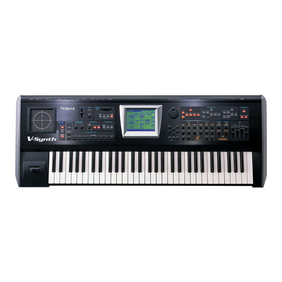
Page 3: Location Of Controls Parts List
V-SYNTH LOCATION OF CONTROLS PARTS LIST [PARTS] PARTCODE PART NAME DESCRIPTION Q’TY 01783956 N S-KEYTOP MD4H 03126856 D S-KEYTOP SX2H-B CLR 3,27 03126867 D S-KEYTOP SX1H-B CLR 03126878 D S-KEYTOP SX1H-B BLK 03126889 D S-KEYTOP SX2H-B BLK 03125589 M R-KNOB... -
Page 4: Location Of Controls
Mar.2003 V-SYNTH LOCATION OF CONTROLS fig.panel... -
Page 5: Exploded View
Mar.2003 V-SYNTH XPLODED VIEW PARTS LIST EXPLODED VIEW [Parts] fig.explo-1 PART CODE PART NAME DESCRIPTION Q,TY 02784778 TOP PANEL 03121112 DISPLAY ESCT 02895601 PAD ESCT 72230178 LCD ASSY 03120690 DISPLAY HOLDER 72230089 PANEL-L KEYTOP ASSY 72230101 PANEL-R KEYTOP ASSY 02674034... - Page 6 Mar.2003 V-SYNTH...
-
Page 7: Parts List
Mar.2003 PARTS LIST fig.part1e CONSIDERATION ON PARTS ORDRING SAFETY PRECAUTIONS: When ordering any parts listed in the parts list, please specify the following items in the order sheet. The parts marked have PART NUMBER DESCRIPTION MODEL NUMBER safety-related characteristics. Use 22575241 Sharp Key C-20/50... - Page 8 V-SYNTH BENDER UNIT 71905023 PB-H0203 BENDER TURBOLESS NOTE: Replacement PB-H0203 should be made on a unit base. SPEAKER, BUZZER 15299147 PKM22EP-2001 BUZZER SP1 on Sub board KEYBOARD ASSY 72232478 KEYBOARD ASSY SK-961-J NOTE: See ‘KEYBOARD PARTS LIST’ for details. PCB ASSY...
- Page 9 Mar.2003 03235312 K4S561632 IC (DRAM) IC3,IC7 on Main board D-TC75 02232367 HN58X2432FPI IC (EEPROM) IC11 on Main board ******** LH28F320BFE-PTBL80 IC (FLASH MEMORY) IC21 on Main board ******** NAND K9F5608U0B IC (FLASH MEMORY) IC509 on Main 02234167 AK4393-VF-E2 IC (DAC) IC546 on Main board 01679990 AK4524VF-E2...
- Page 10 V-SYNTH TRANSISTOR 15129184 RN1207-TPE4 DIGITAL TRANSISTOR Q9,Q10 on Pad Board,Q25,Q24 on Lcd Board 15129215 RN2207-TPE4 DIGITAL TRANSISTOR Q7,Q8 on Pad Board,Q23,Q22 on Lcd Board DIODE 01019534 1SS355 TE-17 SWITCHING DIODE D505 on Main board 01780045 RB051L-40 SCHOTTKY DIODE D501,D1 on Main board...
- Page 11 Mar.2003 RESISTOR 00567289 RPC05T 103 J MTL.FILM RESISTOR R147,R137,R127,R125,R124,R122,R162,R164 ,R171,R176,R506,R196,R502,R120,R52,R507, R513,R514,R515,R517,R522,R662,R46,R35,R 34,R24,R19,R11,R501,R559,R58,R43,R119,R 49,R50,R53, R63,R68,R69,R70,R71,R92,R105,R10,R567,R 580,R581,R645,R661,R195,R566 on Main board,R9 on Panel-L board ,R87,R93,R6,R62,R5,R4,R1,R54,R32,R145,R1 03 on Sub board 00567378 RPC05T 473 J MTL.FILM RESISTOR R571 on Main board ,R61 on Sub board 00567412 RPC05T 104 J MTL.FILM RESISTOR...
- Page 12 V-SYNTH RESISTOR 01906667 MNR14 EOAB J 100 RESISTOR-ARRY RA17,RA2,RA4,RA3,RA6,RA18,RA23,RA2 4 on Sub board 13749817T0 SR25TRE 682 J CARBON RESISTOR R24,R18,R11,R3 on Jack Board 13749851T0 CARBON RESISTOR SR25TRE CARBON RESISTOR R21,R7 on Jack Board 184 J 13749807T0 SR25TRE 272 J CARBON RESISTOR...
- Page 13 Mar.2003 CAPACITOR 01675167 GRM39CH100D50PT CERAMIC CAPACITOR C587,C585,C576,C586 on Main board 01675190 GRM39CH220J50PT CERAMIC CAPACITOR C560,C75,C561 on Main board 01675201 GRM39CH270J50PT CERAMIC CAPACITOR C76 on Main board 01675234 GRM39CH470J50PT CERAMIC CAPACITOR C86,C84,C85 on Main board 01675312 GRM39CH221J50PT CERAMIC CAPACITOR C141 on Main board 01898423 ECHU1H222JX5 POLYEST.
- Page 14 V-SYNTH INDUCTOR, COIL, FILTER 02900945 CR75-220KC CHOKE COIL L2 on Main board 02900956 CR75-100KC CHOKE COIL L512 on Main board 01909645 EXCML16A270U FERRITE-BEAD L505,L501 on Main board 02238212 N2012ZPS121T50 FERRITE-BEAD L520 on Main board 01783590 BLM11B601SPT FERRITE-BEAD L522,L524,L525 on Main board...
- Page 15 Mar.2003 WIRING, CABLE 02679412 WIRING WIRING W2 CN18 on Inverter to CN2 on Power Suply Unit 02566167 BAN CARD BNCD-P=1.25-K-18-450 CN4 on Sub to Keyboard Unit 03121534 BAN CARD BNCD-P=1.25-K-16-450 CN3 on Sub to Keyboard Unit TRANSFORMER 02019478 (7KQ5) 19832A PULSE TRANS T501 on Main board 02457412...
-
Page 16: Checking The Version Number
(Project) Checking the version number in To back up the internal data of the V-Synth, you will use the V-Synth’s USB Patch mode connection in Storage mode to copy all data of the internal disk onto a drive (e.g., hard disk) of your computer. -
Page 17: Restoring The Factory Settings
This returns all data in the V-Synth to the factory settings (Factory Reset). Copy the program ROM file (V-Synth.rom) and the internal image file If data created by the user has already been saved in the V-Synth, all such data (V-SynthDiskImage.bin) from the CD-ROM into the drive that appeared. -
Page 18: Test Mode
If the above steps did not result in a successful update, please check the MA-10D etc. following two points. • Are the V-Synth and computer correctly connected by a USB cable? • Were the correct files copied to the drive that appeared on your CD/MD player etc. - Page 19 Mar.2003 Test item details 2: Beep Test fig.13-3_70 0: Test Mode Top page (Identifying the version number) fig.13-1_70 Verify that a beep is sounded from the internal speaker. • Press [INC] once, and a high-pitched and a low-pitched beep will each sound once.
- Page 20 V-SYNTH 4: MIDI Test fig.13-5_70 • Reinsert the jack, and press [ ] to proceed to the next step. Check MIDI connections. • Use a MIDI cable to connect the MIDI IN and MIDI OUT. Check the DIR OUT output and the INPUT (LINE) input.
- Page 21 Mar.2003 Check DIGITAL OUT 48KHz. • Verify that the all-pixel-on screen is not missing any pixels, and that the darkness is uniform. • Audio at a sampling rate of 48 kHz will be output from the OPTICAL fig.13-9_70 OUT jack. Set your speakers for optical input.
- Page 22 V-SYNTH a confirmation tone will be output. value of 0. • If both rotations are “OK,” you will automatically proceed to the next • If a knob has a center detent, turn it “left-right-center.” Indications of test item. “OK” will be displayed if far left produces a value of 0, far right produces a value of 127, and center (detent) produces a value of 64.
- Page 23 • When the touch has been detected, the box will move to the next point. 15: XY-PAD A/D check • Verify that the V-Synth produces a beep when you touch the screen. fig.13-19_70 • When you have touched all four points on the screen, calibration will be performed.
- Page 24 • Insert a PC card into the PC card slot. 10 cm to 40 cm. Use a PC card (formatted by the V-Synth). • “OK” results will be displayed if a maximum value reaches 127 (10 cm • Press [ ].
- Page 25 Mar.2003 20: Keyboard Test (sounding check / • The lower left of the screen indicates the number of switches yet to be checked. velocity check) • When the switches have been pressed correctly, you will automatically proceed to the next test item. fig.13-24_70 Check the Blue LEDs.
- Page 26 Before the “UsbIdSet.ext” program used with the UM-880 can be used to write the USB ID of the V-Synth, you must add the V-Synth’s ID as shown below A PC is used for this test. Start up “UsbIdSet.exe” before you continue.
- Page 27 A window will appear. fig.13-33_50 Input the following items into the appropriate fields. Model Name V-Synth MIDI IN Roland V-SYNTH MIDI OUT Roland V-SYNTH Test Mode Enter SysEx f0 41 10 00 49 12 4b 03 16 1c f7 Press OK.
-
Page 28: Keyboard Parts List
V-SYNTH KEYBOARD PARTS LIST PART CODE PART NAME DESCRIPTION Q’TY 00893723W0 NATURAL KEY C/F SK-9 (W/WEIGHT) 00893734W0 NATURAL KEY E/B SK-9 (W/WEIGHT) 00893756W0 NATURAL KEY D SK-9 (W/WEIGHT) 00893767W0 NATURAL KEY G SK-9 (W/WEIGHT) 00893745W0 NATURAL KEY A SK-9 (W/WEIGHT) 00893778W0 NATURAL KEY C’/F’... -
Page 29: Keyboard Circuit Board
Mar.2003 V-SYNTH KEYBOARD CIRCUIT BOARD fig.keyboard-board KEYBOARD CIRCUIT DIAGRAM fig.keyboard-circit... -
Page 30: Keyboard Disassembly
Mar.2003 KEYBOARD DISASSEMBLY <Attaching the RUBBER SWITCHES and PCB> To fasten the SK-9 PWB,be sure to use 3*10mm BINDING VWH (PART No.40233545). Turn the chassis over as shown in fig.1.Next,place 4 pieces of RUBBER SWITCH 12P in turn,on the chassis from the left end(the bass side of keyboard),aligning them with the long holes provided on the chassis. - Page 31 V-SYNTH Then,using the screws,fasten the LOW and HI PCBs to the chassis from the center of the keyboard,that is,from the LOW PCB as shown in fig.5.While you are screwing down the PCB,it may float from the chassis.To avoid this,after screwing in the PCB at the center of the keyboard,screw down opposite end,before screwing in other areas in the middle of the PCB.(See fig.5)In addition,the PCBs may be warped by...
-
Page 32: Block Diagram
Mar.2003 V-SYNTH BLOCK DIAGRAM fig.block Back Light CN29 power MAIN BOARD 11.08335 MHz IC501 100V/117V/230V/240V TOUCH & LCDC PANEL IC3,7 IC21 IC509 M66273AFP TOUCH PANEL NAND 133MHz 22.1667MHz SDRAM FLASH FLASH 256Mbit x 2 12x350-P2.0-PHR-PHR-F 32Mbit 256Mbit LCD BOARD CN506... -
Page 33: Circuit Board(Main)
Mar.2003 CIRCUIT BOARD(MAIN) fig.main-1... - Page 34 V-SYNTH fig.main-1 scale=0.9...
-
Page 35: Circuit Diagram(Mian 1)
Mar.2003 V-SYNTH CIRCUIT DIAGRAM(MIAN 1) fig.main-1 D 3.3 D 3.3 CA[0..25] VDD-PLL1 VDD-RTC C2 10/6.3 CA24 10/6.3 D 3.3 CA24 CA25 CA25 VSS-PLL1 VSS-RTC D 3.3 D 3.3 D 3.3 BCA[0..23] BCA[0..23] HD74LV245AT D 3.3 D 3.3 CA25 100/16 R3 100... -
Page 36: Circuit Diagram(Mian 2)
Mar.2003 V-SYNTH CIRCUIT DIAGRAM(MIAN 2) fig.main-2 BCA[0..23] BCA[0..23] BCD[0..31] BCD[0..31] D 3.3 C100 0.1 C101 0.1 C102 0.1 C103 0.1 C104 0.1 C105 0.1 CA25 CA25 C106 0.1 CA24 CA24 D 3.3 BCA23 BCA23 BCA22 BCA22 C107 D 3.3 D 3.3... -
Page 37: Circuit Diagram(Mian 3)
Mar.2003 V-SYNTH CIRCUIT DIAGRAM(MIAN 3) fig.main-3 D 3.3 R501 D 3.3 TP501 C501 10/16 D 3.3 C508 C502 100/16 C503 JK501 C504 YKF45-0020 BCA[1..14] C505 BCA[1..14] C506 C510 BCD[0..15] C507 3V --> 5V BCD[0..15] C682 C509 C511 IC501 C512 M66273FP BCA[1..6]... -
Page 38: Circuit Diagram(Mian 4)
Mar.2003 V-SYNTH CIRCUIT DIAGRAM(MIAN 4) fig.main-4 NAND FLASH (WAVE MEMORY) IDE (OPTION) D 3.3 3.3V <--> 5V BCD[0..15] BCD[0..7] C536 C538 BCD[0..7] D 3.3 100/16 C537 IDED[0..15] NAND FLASH IC509 BCD7 BCD15 IDED15 I/O8 BCD6 BCD0 IDED0 I/O7 BCD5 BCD14... -
Page 39: Circuit Diagram(Mian 5)
Mar.2003 V-SYNTH CIRCUIT DIAGRAM(MIAN 5) fig.main-5 PCMCIA CA25 CA24 BCA[23..0] BCA[23..0] From C_D[0..15] BCD[15..0] BCD[15..0] D 3.3 D 3.3 L513 L514 CARD_POWER C552 C553 IC520 RA507 RA508 CARD_POWER HD74LV245AT R565 R564 BCD10 C_D10 C_D11 100K 100K C_A[25..0] BCD9 C_D9 C_D12... -
Page 40: Circuit Board(Panel L)
Mar.2003 CIRCUIT BOARD(PANEL L) fig.panel-l... - Page 41 V-SYNTH fig.panel-l...
-
Page 42: Circuit Diagram(Panel L)
Mar.2003 V-SYNTH CIRCUIT DIAGRAM(PANEL L) fig.panel-l MA142WK-(TX) DA24 MA142WK-(TX) MA142WK-(TX) 3.3k 0.47 6.8k TPS706 MA142WK-(TX) to SUB BOARD DBEAM 4700p 2.2k (CN12) SSS5 SSS4 IC5B SSS3 NJM2904M SSS2 SSS1 IC1A IC1B IC2A IC2B 33000p 3.3k 4700p SSS0 UPC4570G UPC4570G UPC4570G... -
Page 43: Circuit Board(Panel R)
Mar.2003 CIRCUIT BOARD(PANEL R) fig.panel-r... - Page 44 V-SYNTH fig.panel-r...
-
Page 45: Circuit Diagram(Panel R)
Mar.2003 V-SYNTH CIRCUIT DIAGRAM(PANEL R) fig.panel-r EN1A EN1B EC12E2420802 EC12E2420802 VR1A VR2A VR3A VR4A VR5A VR6A VR7A VR8A RK09D1130 RK09D1130 RK09D1130 RK09D1130 RK09D1130 RK09D1130 RK09D1130 RK09D1130 10KB 2 10KB 2 10KB 2 10KB 2 10KB 2 10KB 2 10KB 2... -
Page 46: Circuit Board(Relay)
Mar.2003 V-SYNTH CIRCUIT BOARD(RELAY) fig.panel-r... -
Page 47: Circuit Diagram(Relay)
Mar.2003 V-SYNTH CIRCUIT DIAGRAM(RELAY) fig.rely INVERTER BOARD LCD BOARD ASSY 72230156 ASSY 72230145 A+15V to MAIN BOARD from SWITCHING REGULATOR (CN501) CN18 CN19 to LCD UINT to MAIN BOARD CN16 CN17 AGND (CN502) A-15V B7B-XH-A B7B-XH-A D+5V LCDVEE B12B-PH-K-S 12FE-BT-VK-N... -
Page 48: Circuit Board(Sub)
Mar.2003 CIRCUIT BOARD(SUB) fig.rely... - Page 49 V-SYNTH fig.rely...
-
Page 50: Circuit Diagram(Sub-1)
Mar.2003 V-SYNTH CIRCUIT DIAGRAM(SUB-1) fig.sub-1 C106 YKF51-5041 2.2k MA147-(TX) MIDI_IN C114 C115 IC17 470/16 PC410LKNIP DTA114EUA R100 R101 5.1MB XRST_SUB IC19A PKM22EP-2001 HD74LV05AFPEL MA147-(TX) R102 R103 5.1MB MIDI_OUT DTC114EUA IC19B IC19C HD74LV05AFPEL HD74LV05AFPEL MA147-(TX) R142 4.7k MIDI_IN BUZZER IC19E IC19D... -
Page 51: Circuit Diagram(Sub-2)
Mar.2003 V-SYNTH CIRCUIT DIAGRAM(SUB-2) fig.sub-2 LS[0..3] AN_SEL[0..3] IC15 LD[0..7] HD74HC138FPEL R123 LLS7 LLS6 AN_SELB3 LLS5 AN_SEL3 LLS4 IC14A LLS3 TC74HC08AF(EL) LLS2 LLS1 R128 LLS0 AN_SELB2 AN_SEL2 IC14B TC74HC08AF(EL) R149 R158 AN_SELB3 R129 IC14E TC74HC08AF(EL) AN_SELB1 R151 R155 R156 R157 AN_SEL1... -
Page 52: Error Messages
The media is of a for- Prepare a media that File Write Error! mat to which the V- is of a format to which Synth cannot write. the V-Synth is able to write. DISK Since the format of Do not use this file. Illegal Format! this file is incorrect, it cannot be loaded.
Need help?
Do you have a question about the V-Synth and is the answer not in the manual?
Questions and answers