Table of Contents
Advertisement
Quick Links
Advertisement
Table of Contents

Related Manuals for Cinterion MC75i


Summary of Contents for Cinterion MC75i
- Page 1 MC75i Version: 01.100a DocId: MC75i_HD_v01.100a...
- Page 2 UCT") IS SUBJECT TO THE RELEASE NOTE PROVIDED TOGETHER WITH PRODUCT. IN ANY EVENT THE PROVISIONS OF THE RELEASE NOTE SHALL PREVAIL. THIS DOCUMENT CONTAINS INFORMATION ON CINTERION PRODUCTS. THE SPECIFICATIONS IN THIS DOCUMENT ARE SUB- JECT TO CHANGE AT CINTERION'S DISCRETION. CINTERION WIRELESS MODULES GMBH GRANTS A NON-EXCLUSIVE RIGHT TO USE THE PRODUCT.
-
Page 3: Table Of Contents
3.3.1.3 Turn on MC75i Using the VCHARGE Signal....... 30 3.3.1.4 Reset MC75i via AT+CFUN Command....... 31 3.3.1.5 Reset or Turn off MC75i in Case of Emergency....31 3.3.1.6 Using EMERG_OFF Signal to Reset Application(s) or External Device(s) ............... 31 3.3.2 Signal States after Startup .............. - Page 4 MC75i Hardware Interface Description Contents 3.5.5 Charger Requirements................ 44 3.5.6 Implemented Charging Technique............44 3.5.7 Operating Modes during Charging............45 Power Saving....................47 3.6.1 Network Dependency of SLEEP Modes ..........47 3.6.2 Timing of the CTSx Signal in CYCLIC SLEEP Mode 7....... 48 3.6.3...
- Page 5 Air Interface....................100 Electrostatic Discharge .................. 101 Mechanics........................ 102 Mechanical Dimensions of MC75i..............102 Mounting MC75i to the Application Platform ..........104 Board-to-Board Application Connector ............105 Sample Application....................109 Reference Approval ....................111 Reference Equipment for Type Approval............111 Compliance with FCC and IC Rules and Regulations ........
- Page 6 Return loss in the active band................ 72 Table 20: Product specifications of MC75i antenna connectors ........75 Table 21: Material and finish of MC75i antenna connectors and recommended plugs . 76 Table 22: Ordering information for Hirose U.FL Series..........78 Table 23: Absolute maximum ratings................
- Page 7 Figure 18: USB circuit ..................... 55 Figure 19: C interface connected to VCC of application ..........56 Figure 20: C interface connected to VEXT line of MC75i ..........56 Figure 21: SPI interface....................57 Figure 22: Characteristics of SPI modes................. 58 Figure 23: Audio block diagram..................
-
Page 8: Document History
Revised values for RTC backup in Table Updated tables listing power supply ratings. Added IC label. New section showing an optional mounting clip for MC75i. Preceding document: "MC75i Hardware Interface Description" Version 00.031 New document: "MC75i Hardware Interface Description" Version 00.200 Chapter... - Page 9 Updated Table Table 39: Updated specifications of measured electrostatic values. Added more detailed description related to test equipment for FCC tests. New document: "MC75i Hardware Interface Description" Version 00.031 Chapter What is new Initial document setup. MC75i_HD_v01.100a Page 9 of 122...
-
Page 10: Introduction
Introduction This document describes the hardware of the Cinterion MC75i module that connects to the cellular device application and the air interface. It helps you quickly retrieve interface specifica- tions, electrical and mechanical details and information on the requirements to be considered for integrating further components. - Page 11 Digital-to-Analog Converter Digital Audio Interface dBm0 Digital level, 3.14dBm0 corresponds to full scale, see ITU G.711, A-law Data Communication Equipment (typically modems, e.g. Cinterion GSM module) DCS 1800 Digital Cellular System, also referred to as PCN Discontinuous Reception Development Support Box...
- Page 12 MC75i Hardware Interface Description 1.2 Terms and Abbreviations Abbreviation Description International Telecommunications Union kbps kbits per second Light Emitting Diode Li-Ion / Li+ Lithium-Ion Li battery Rechargeable Lithium Ion or Lithium Polymer battery Mbps Mbits per second Man Machine Interface...
- Page 13 MC75i Hardware Interface Description 1.2 Terms and Abbreviations Abbreviation Description SELV Safety Extra Low Voltage Subscriber Identification Module Short Message Service Serial Peripheral Interface SRAM Static Random Access Memory Terminal adapter (e.g. GSM module) TDMA Time Division Multiple Access...
-
Page 14: Regulatory And Type Approval Information
1.3.1 Directives and Standards MC75i is designed to comply with the directives and standards listed below. It is the responsibility of the application manufacturer to ensure compliance of the final product with all provisions of the applicable directives and standards as well as with the technical spec- ifications provided in the "MC75i Hardware Interface Description". -
Page 15: Table 4: Requirements Of Quality
MC75i Hardware Interface Description 1.3 Regulatory and Type Approval Information Table 3: Standards of European type approval ETSI EN 301 489-7 Candidate Harmonized European Standard (Telecommunications series) V1.2.1 (2000-09) Electro Magnetic Compatibility and Radio spectrum Matters (ERM); Elec- tro Magnetic Compatibility (EMC) standard for radio equipment and ser- vices;... -
Page 16: Sar Requirements Specific To Portable Mobiles
Mobile phones, PDAs or other portable transmitters and receivers incorporating a GSM module must be in accordance with the guidelines for human exposure to radio frequency energy. This requires the Specific Absorption Rate (SAR) of portable MC75i based applications to be eval- uated and approved for compliance with national and/or international regulations. -
Page 17: Safety Precautions
The following safety precautions must be observed during all phases of the operation, usage, service or repair of any cellular terminal or mobile incorporating MC75i. Manufacturers of the cellular terminal are advised to convey the following safety information to users and operating personnel and to incorporate these guidelines into all manuals supplied with the product. -
Page 18: Product Concept
MC75i Hardware Interface Description 2 Product Concept Product Concept Key Features at a Glance Feature Implementation General Frequency bands Quad band: GSM 850/900/1800/1900MHz GSM class Small MS Output power (according Class 4 (+33dBm ±2dB) for EGSM850 to Release 99) Class 4 (+33dBm ±2dB) for EGSM900... - Page 19 Access by AT commands Remote SIM Access MC75i supports Remote SIM Access. RSA enables MC75i to use a remote SIM card via its serial interface and an external application, in addition to the SIM card locally attached to the dedicated lines of the application inter- face.
- Page 20 Phonebook SIM and phone TTY/CTM support Integrated CTM modem Evaluation kit DSB75 DSB75 Evaluation Board designed to test and type approve Cinterion Wire- less Modules and provide a sample configuration for application engineer- ing. MC75i_HD_v01.100a Page 20 of 122 2009-08-13...
-
Page 21: Mc75I System Overview
MC75i Hardware Interface Description 2.2 MC75i System Overview MC75i System Overview Figure 1: MC75i system overview MC75i_HD_v01.100a Page 21 of 122 2009-08-13 Confidential / Released... -
Page 22: Circuit Concept
MC75i Hardware Interface Description 2.3 Circuit Concept Circuit Concept Figure 2 shows a block diagram of the MC75i module and illustrates the major functional com- ponents: Baseband block: • Digital baseband processor with DSP • Analog processor with power supply unit (PSU) •... -
Page 23: Application Interface
MC75i Hardware Interface Description 3 Application Interface Application Interface MC75i is equipped with an 80-pin board-to-board connector that connects to the external ap- plication. The host interface incorporates several sub-interfaces described in the following sec- tions: • Power supply - see Section 3.2... -
Page 24: Operating Modes
MC75i Hardware Interface Description 3.1 Operating Modes Operating Modes The table below briefly summarizes the various operating modes referred to in the following chapters. Table 7: Overview of operating modes Normal operation GSM / GPRS SLEEP Various power save modes set with AT+CFUN command. -
Page 25: Power Supply
MC75i needs to be connected to a power supply at the board-to-board connector (5 lines each BATT+ and GND). The power supply of MC75i has to be a single voltage source at BATT+. It must be able to pro- vide the peak current during the uplink transmission. -
Page 26: Measuring The Supply Voltage Vbatt
RF interface. The duration of measuring ranges from 0.5s in TALK/DATA mode to 50s when MC75i is in IDLE mode or Limited Service (deregistered). The displayed voltage (in mV) is averaged over the last measuring period before the AT^SBV command was executed. -
Page 27: Power Up / Power Down Scenarios
MC75i Hardware Interface Description 3.3 Power Up / Power Down Scenarios Power Up / Power Down Scenarios In general, be sure not to turn on MC75i while it is beyond the safety limits of voltage and tem- perature stated in Chapter 5. -
Page 28: Figure 5: Powerup With Operating Voltage At Batt+ Applied Before Activating Igt
AT\Q or AT+IFC (see for details). The default setting of MC75i is AT\Q0 (no flow control) which shall be altered to AT\Q3 (RTS/CTS handshake). If the application design does not integrate RTS/CTS lines the host application shall wait at least for the “^SYSSTART”... -
Page 29: Figure 6: Powerup With Igt Held Low Before Switching On Operating Voltage At Batt
MC75i Hardware Interface Description 3.3 Power Up / Power Down Scenarios For details on how to use EMERG_OFF to reset ap- plications or external devices see Section 3.3.1.6. Figure 6: Powerup with IGT held low before switching on operating voltage at BATT+ MC75i_HD_v01.100a... -
Page 30: Configuring The Igt Line For Use As On/Off Switch
To ensure that the IGT line works properly as ON/OFF switch it is of vital importance that the following conditions are met. Switch-on condition:If the MC75i is off, the IGT line must be asserted for at least 400ms before being released. The module switches on after 400ms. -
Page 31: Reset Mc75I Via At+Cfun Command
MC75i Hardware Interface Description 3.3 Power Up / Power Down Scenarios During the Charge-only mode MC75i is neither logged on to the GSM network nor are the serial interfaces fully accessible. To switch from Charge-only mode to Normal mode the ignition line (IGT) must be pulled low for at least 2 seconds. -
Page 32: Signal States After Startup
MC75i Hardware Interface Description 3.3 Power Up / Power Down Scenarios 3.3.2 Signal States after Startup Table 8 describes the various states each interface signal passes through after startup and dur- ing operation. As shown in Figure 5 Figure 6 signals are in an undefined state while the module is initial- izing. - Page 33 MC75i Hardware Interface Description 3.3 Power Up / Power Down Scenarios Table 8: Signal states Signal name Undefined state Defined state Active state after configuration by AT during startup after startup ini- command tialization DAI4 Tristate DAI5 Tristate DAI6 Tristate 1.
-
Page 34: Turn Off Mc75I
The best and safest approach to powering down MC75i is to issue the AT^SMSO command. This procedure lets MC75i log off from the network and allows the software to enter into a se- cure state and safe data before disconnecting the power supply. The mode is referred to as Power-down mode. -
Page 35: Figure 8: Signal States During Turn-Off Procedure
MC75i Hardware Interface Description 3.3 Power Up / Power Down Scenarios Figure 8: Signal states during turn-off procedure Note 1: Depending on capacitance load from host application. MC75i_HD_v01.100a Page 35 of 122 2009-08-13 Confidential / Released... -
Page 36: Turn On/Off Mc75I Applications With Integrated Usb
Turn on/off MC75i Applications with Integrated USB In a Windows environment, the USB COM port emulation causes the USB port of MC75i to ap- pear as a virtual COM port (VCOM port). The VCOM port emulation is only present when Win- dows can communicate with the module, and is lost when the module shuts down. -
Page 37: Thermal Shutdown
The values detected by either NTC resistor are measured directly on the board or the battery and therefore, are not fully identical with the ambient temperature. Each time the board or battery temperature goes out of range or back to normal, MC75i instant- ly displays an alert (if enabled). -
Page 38: Deferred Shutdown At Extreme Temperature Conditions
MC75i Hardware Interface Description 3.3 Power Up / Power Down Scenarios 3.3.4.2 Deferred Shutdown at Extreme Temperature Conditions In the following cases, automatic shutdown will be deferred if a critical temperature limit is ex- ceeded: • While an emergency call is in progress. -
Page 39: Overvoltage Shutdown
Keep in mind that several MC75i components are directly linked to BATT+ and, therefore, the supply voltage remains applied at major parts of MC75i, even if the module is switched off. Es- pecially the power amplifier is very sensitive to high voltage and might even be destroyed. -
Page 40: Automatic Gprs Multislot Class Change
This reduces the power consumption and, consequently, causes the board’s temperature to decrease. Once the temperature drops by 5 degrees, MC75i returns to the higher Multislot Class. If the temperature stays at the critical level or even continues to rise, MC75i will not switch back to the higher class. -
Page 41: Charging Control
GSM/GPRS applications. 3.5.1 Hardware Requirements MC75i has no on-board charging circuit. To benefit from the implemented charging management you are required to install a charging circuit within your application according to the Figure 3.5.2 Software Requirements Use the command AT^SBC, parameter <current>, to enter the current consumption of the host... -
Page 42: Battery Pack Requirements
Table 10. It is recommended that the battery pack you want to integrate into your MC75i application is compliant with these specifications. This ensures re- liable operation, proper charging and, particularly, allows you to monitor the battery capacity using the AT^SBC command. Failure to comply with these specifications might cause AT^SBC to deliver incorrect battery capacity values. -
Page 43: Batteries Tested For Use With Mc75I
3.5.4 Batteries Tested for Use with MC75i When you choose a battery for your MC75i application you can take advantage of one of the following two batteries offered by VARTA Microbattery GmbH. Both batteries meet all require- ments listed above. They have been thoroughly tested by Cinterion Wireless Modules and proved to be suited for MC75i. -
Page 44: Charger Requirements
Duration of charging: • MC75i provides a software controlled timer set to 4 hours as a safety feature to prevent per- manent charging of defective batteries. The duration of software controlled charging depends on the battery capacity and the level of discharge. Normally, charging stops when the battery is fully charged or, at the latest, when the software timer expires after 4 hours. -
Page 45: Operating Modes During Charging
If the charger is connected to the charger input of the external charging circuit and the module’s VCHARGE line while MC75i is in Power-down mode, MC75i goes into Charge-only mode. While the charger remains connected it is not possible to switch the module off by using the AT^SMSO command or the automatic shutdown mechanism. -
Page 46: Table 12: Comparison Charge-Only And Charge Mode
Battery can be charged while GSM module Charge host application charging circuit and remains operational and registered to the mode module’s VCHARGE line while MC75i GSM network. • In IDLE and TALK mode, the serial inter- • operating, e.g. in IDLE or TALK faces are accessible. -
Page 47: Power Saving
CLIC SLEEP mode is that the serial interface remains accessible and that, in intermittent wake- up periods, characters can be sent or received without terminating the selected mode. This al- lows the MC75i to wake up for the duration of an event and, afterwards, to resume power sav- ing. Please refer to for a summary of all SLEEP modes and the different ways of waking up the module. -
Page 48: Timing Of The Ctsx Signal In Cyclic Sleep Mode 7
MC75i Hardware Interface Description 3.6 Power Saving 3.6.2 Timing of the CTSx Signal in CYCLIC SLEEP Mode 7 Figure 11 illustrates the CTSx signal timing in CYCLIC SLEEP mode 7 (CFUN=7). Figure 11: Timing of CTSx signal (if CFUN= 7) With regard to programming or using timeouts, the UART must take the varying CTS inactivity periods into account. -
Page 49: Summary Of State Transitions (Except Sleep Mode)
MC75i Hardware Interface Description 3.7 Summary of State Transitions (Except SLEEP Mode) Summary of State Transitions (Except SLEEP Mode) The following table shows how to proceed from one mode to another (grey column = present mode, white columns = intended modes). -
Page 50: Rtc Backup
The internal Real Time Clock of MC75i is supplied from a separate voltage regulator in the an- alog controller which is also active when MC75i is in POWER DOWN status. An alarm function is provided that allows to wake up MC75i to Airplane mode without logging on to the GSM net- work. -
Page 51: Sim Interface
To take advantage of this feature, an appropriate SIM card detect switch is required on the card holder. For example, this is true for the model supplied by Molex, which has been test- ed to operate with MC75i and is part of the Cinterion Wireless Modules reference equipment submitted for type approval. See Chapter 8 for Molex ordering numbers. -
Page 52: Serial Interface Asc0
The significant levels are 0V (for low data bit or active state) and 2.9V (for high data bit or in- active state). For electrical characteristics please refer to Table MC75i is designed for use as a DCE. Based on the conventions for DCE-DTE connections it communicates with the customer application (DTE) using the following signals: •... -
Page 53: Table 15: Dce-Dte Wiring Of Asc0
MC75i Hardware Interface Description 3.10 Serial Interface ASC0 Table 15: DCE-DTE wiring of ASC0 V.24 circuit DCE Line function Signal direction Line function Signal direction TXD0 Input Output RXD0 Output Input RTS0 Input Output CTS0 Output Input 108/2 DTR0... -
Page 54: Serial Interface Asc1
0V (for low data bit or active state) and 2.9V (for high data bit or inactive state). For electrical characteristics please refer to Table MC75i is designed for use as a DCE. Based on the conventions for DCE-DTE connections it communicates with the customer application (DTE) using the following signals: •... -
Page 55: Usb Interface
The USB host is responsible for supplying, across the VUSB_IN line, power to the module’s USB interface, but not to other MC75i interfaces. This is because MC75i is designed as a self- powered device compliant with the “Universal Serial Bus Specification Revision 2.0”... -
Page 56: I 2 C Interface
I2CDAT and the serial clock line I2CCLK. The MC75i module acts as a single master device, e.g. the clock I2CCLK is driven by module. I2CDAT is a bi-directional line. Each device connected to the bus is software addressable by a unique 7-bit address, and simple master/slave relationships exist at all times. -
Page 57: Spi Interface
SPIDI/SPIDO, the clock line SPICLK and the chip se- lect line SPICS. The MC75i module acts as a single master device, e.g. the clock SPICLK is driven by module. Whenever the SPICS line is in a low state, the SPI bus is activated and data can be transferred from the module and vice versa. -
Page 58: Figure 22: Characteristics Of Spi Modes
MC75i Hardware Interface Description 3.14 SPI Interface Figure 22: Characteristics of SPI modes MC75i_HD_v01.100a Page 58 of 122 2009-08-13 Confidential / Released... -
Page 59: Audio Interfaces
5 can be used for direct access to the speech coder without signal pre or post processing. When shipped from factory, all audio parameters of MC75i are set to interface 1 and audio mode 1. This is the default configuration optimized for the Votronic HH-SI-30.3/V1.1/0 handset and used for type approving the Cinterion Wireless Modules reference configuration. -
Page 60: Speech Processing
As there is less current flowing than through other GND lines of the module or the application, this solution will avoid hum and buzz problems. While MC75i is in Power-down mode, the input voltage at any MIC line must not exceed ±0.3V relative to AGND (see also Section 5.1). -
Page 61: Single-Ended Microphone Input
MC75i Hardware Interface Description 3.15 Audio Interfaces 3.15.2.1 Single-ended Microphone Input Figure 24 as well as Figure 49 show an example of how to integrate a single-ended microphone input. = typ. 2k = typ. 5k = typ. 470Ohm VMIC = typ. -
Page 62: Differential Microphone Input
MC75i Hardware Interface Description 3.15 Audio Interfaces 3.15.2.2 Differential Microphone Input Figure 25 shows a differential solution for connecting an electret microphone. = typ. 1k = 470Ohm VMIC = typ. 100nF = typ. 22µF = typ. 2.5V Vbias = 1.0V … 1.6V, typ. -
Page 63: Line Input Configuration With Opamp
MC75i Hardware Interface Description 3.15 Audio Interfaces 3.15.2.3 Line Input Configuration with OpAmp Figure 26 shows an example of how to connect an opamp into the microphone circuit. = typ. 47k = 470Ohm VMIC = typ. 100nF = typ. 22µF = typ. -
Page 64: Loudspeaker Circuit
MC75i Hardware Interface Description 3.15 Audio Interfaces 3.15.3 Loudspeaker Circuit The GSM module comprises two analog differential speaker outputs: EP1 and EP2. Output EP1 is able to drive a load of 8Ohms while the output EP2 can drive a load of 32Ohms. Inter- face EP2 can also be connected in single ended configuration. -
Page 65: Table 17: Configuration Combinations For The Pcm Interface
MC75i Hardware Interface Description 3.15 Audio Interfaces For the PCM interface configuration the parameters <clock>, <mode> and <framemode> of the AT^SAIC command are used. The following table lists possible combinations: Table 17: Configuration combinations for the PCM interface Configuration <clock>... -
Page 66: Master Mode
MC75i Hardware Interface Description 3.15 Audio Interfaces 3.15.4.1 Master Mode To clock input and output PCM samples the PCM interface delivers a bit clock (BITCLK) which is synchronous to the GSM system clock. The frequency of the bit clock is 256kHz or 512kHz. -
Page 67: Slave Mode
MC75i Hardware Interface Description 3.15 Audio Interfaces The timing of a PCM long frame is shown in Figure 30. The 16-bit TXDAI and RXDAI data is transferred simultaneously in both directions while the frame sync pulse FS is high. For this rea- son the duration of a frame sync pulse is 16 BITCLK periods, starting at the rising edge of BIT- CLK. -
Page 68: Figure 31: Slave Pcm Interface Application
MC75i Hardware Interface Description 3.15 Audio Interfaces Figure 31: Slave PCM interface application The following figures show the slave short and long frame timings. Because these are edge controlled, frame sync signals may deviate from the ideally form as shown with the dotted lines. -
Page 69: Control Signals
Your platform design must be such that the incoming signal accommodates sufficient power supply to the MC75i module if required. This can be achieved by lowering the current drawn from other components installed in your application. -
Page 70: Using The Sync Line To Control A Status Led
As an alternative to generating the synchronization signal, the SYNC line can be configured to drive a status LED that indicates different operating modes of the MC75i module. To take ad- vantage of this function the LED mode must be activated with the AT^SSYNC command and the LED must be connected to the host application. -
Page 71: Behavior Of The Ring0 Line (Asc0 Interface Only)
MC75i Hardware Interface Description 3.16 Control Signals 3.16.3 Behavior of the RING0 Line (ASC0 Interface only) The RING0 line is available on the first serial interface ASC0 (see also Section 3.10). The sig- nal serves to indicate incoming calls and other types of URCs (Unsolicited Result Code). -
Page 72: Antenna Interface
The external antenna must be matched properly to achieve best performance regarding radi- ated power, DC-power consumption, modulation accuracy and harmonic suppression. Anten- na matching networks are not included on the MC75i module and should be placed in the host application. -
Page 73: Figure 38: Never Use Antenna Connector And Antenna Pad At The Same Time
MC75i Hardware Interface Description 4.1 Antenna Installation Antenna connected to Hirose connector: Antenna connected to pad: Figure 38: Never use antenna connector and antenna pad at the same time No matter which option you choose, ensure that the antenna pad does not come into contact with the holding device or any other components of the host application. -
Page 74: Antenna Pad
Antenna Pad The antenna can be soldered to the pad, or attached via contact springs. For proper grounding connect the antenna to the ground plane on the bottom of MC75i which must be connected to the ground plane of the application. -
Page 75: Antenna Connector
Figure 40). Minor differences in product specifications are mentioned in Table 20. The position of the antenna connector on the MC75i board can be seen in Figure Figure 40: Mechanical dimensions of MC75i antenna connectors Table 20: Product specifications of MC75i antenna connectors... -
Page 76: Table 21: Material And Finish Of Mc75I Antenna Connectors And Recommended Plugs
MC75i Hardware Interface Description 4.3 Antenna Connector Table 21: Material and finish of MC75i antenna connectors and recommended plugs Part Material Finish Shell Phosphor bronze Hirose: Silver plating Molex: Gold plating Male center contact Brass Gold plating Female center contact... -
Page 77: Figure 43: Specifications Of U.fl-Lp-(V)-040(01) Plug
MC75i Hardware Interface Description 4.3 Antenna Connector In addition to the connectors illustrated above, the U.FL-LP-(V)-040(01) version is offered as an extremely space saving solution. This plug is intended for use with extra fine cable (up to 0.81mm) and minimizes the mating height to 2mm. See... -
Page 78: Table 22: Ordering Information For Hirose U.fl Series
MC75i Hardware Interface Description 4.3 Antenna Connector Table 22: Ordering information for Hirose U.FL Series Item Part number HRS number Connector on MC75i U.FL-R-SMT CL331-0471-0-10 Right-angle plug shell for U.FL-LP-040 CL331-0451-2 Ø 0.81mm cable Right-angle plug for U.FL-LP(V)-040 (01) CL331-053-8-01 Ø... -
Page 79: Electrical, Reliability And Radio Characteristics
Absolute Maximum Ratings The absolute maximum ratings stated in Table 23 are stress ratings under any conditions. Stresses beyond any of these limits will cause permanent damage to MC75i. Table 23: Absolute maximum ratings Parameter Unit Peak current of power supply Supply voltage BATT+ -0.3... -
Page 80: Operating Temperatures
• When data are transmitted over EGPRS or GPRS the MC75i automatically reverts to a lower Multislot Class if the temperature increases to the limit specified for normal operation and, vice versa, returns to the higher Multislot Class if the temperature is back to normal. -
Page 81: Storage Conditions
MC75i Hardware Interface Description 5.3 Storage Conditions Storage Conditions The conditions stated below are only valid for modules in their original packed state in weather protected, non-temperature-controlled storage locations. Normal storage time under these conditions is 12 months maximum. -
Page 82: Reliability Characteristics
MC75i Hardware Interface Description 5.4 Reliability Characteristics Reliability Characteristics The test conditions stated below are an extract of the complete test specifications. Table 28: Summary of reliability test conditions Type of test Conditions Standard Vibration Frequency range: 10-20Hz; acceleration: 5g DIN IEC 68-2-6 Frequency range: 20-500Hz;... -
Page 83: Pin Assignment And Signal Description
MC75i Hardware Interface Description 5.5 Pin Assignment and Signal Description Pin Assignment and Signal Description The Molex board-to-board connector on MC75i is an 80-pin double-row receptacle. The loca- tion of the pins can be seen from Figure 45 which shows the top view of MC75i. -
Page 84: Table 30: Signal Description
5.5 Pin Assignment and Signal Description Please note that the reference voltages listed in Table 30 are the values measured directly on the MC75i module. They do not apply to the accessories connected. Table 30: Signal description Function Signal name Signal form and level... - Page 85 MC75i Hardware Interface Description 5.5 Pin Assignment and Signal Description Table 30: Signal description (Continued) Function Signal name Signal form and level Comment External VEXT Normal mode: VEXT may be used for applica- supply min = 2.75V tion circuits, for example to sup- voltage typ = 2.93V...
- Page 86 4.616ms, with 180µs forward time. ent during handover. b) Driving a status LED to indi- cate different operating modes of MC75i. The LED must be installed in the host application. To select a) or b) use the AT^SSYNC command. If unused keep line open.
- Page 87 MC75i Hardware Interface Description 5.5 Pin Assignment and Signal Description Table 30: Signal description (Continued) Function Signal name Signal form and level Comment ASC0 RXD0 max = 0.2V at I = 2mA Serial interface for AT com- Serial min = 2.55V at I = -0.5mA mands or data stream.
- Page 88 MC75i Hardware Interface Description 5.5 Pin Assignment and Signal Description Table 30: Signal description (Continued) Function Signal name Signal form and level Comment CCIN 100k CCIN = Low, SIM card holder interface max = 0.6V at I = -25µA...
- Page 89 MC75i Hardware Interface Description 5.5 Pin Assignment and Signal Description Table 30: Signal description (Continued) Function Signal name Signal form and level Comment SPIDI max = 0.2V at I = 2mA If the Serial Peripheral Interface Serial min = 2.55V at I = -0.5mA...
- Page 90 MC75i Hardware Interface Description 5.5 Pin Assignment and Signal Description Table 30: Signal description (Continued) Function Signal name Signal form and level Comment Analog VMIC min = 2.4V Microphone supply for cus- Audio typ = 2.5V tomer feeding circuits interface max = 2.6V...
-
Page 91: Power Supply Ratings
MC75i Hardware Interface Description 5.6 Power Supply Ratings Power Supply Ratings Table 31: Power supply ratings Parameter Description Conditions Unit BATT+ Supply voltage Directly measured at reference point TP BATT+ and TP GND, see Section 3.2.2. Voltage must stay within the min/max values, including voltage drop, ripple, spikes. -
Page 92: Table 32: Current Consumption During Tx Burst For Gsm 850Mhz And Gsm 900Mhz
MC75i Hardware Interface Description 5.6 Power Supply Ratings Table 32: Current consumption during Tx burst for GSM 850MHz and GSM 900MHz Mode GSM call GPRS GPRS Class10 GPRS Class 12 EPGRS EGPRS Class 10 EGPRS Class 12 Class 8... -
Page 93: Table 33: Current Consumption During Tx Burst For Gsm 1800Mhz And Gsm 1900Mhz
MC75i Hardware Interface Description 5.6 Power Supply Ratings Table 33: Current consumption during Tx burst for GSM 1800MHz and GSM 1900MHz Mode GSM call GPRS GPRS Class10 GPRS Class 12 EPGRS EGPRS Class 10 EGPRS Class 12 Class 8... -
Page 94: Electrical Characteristics Of The Voiceband Part
MC75i Hardware Interface Description 5.7 Electrical Characteristics of the Voiceband Part Electrical Characteristics of the Voiceband Part 5.7.1 Setting Audio Parameters by AT Commands The audio modes 2 to 6 can be adjusted according to the parameters listed below. Each audio mode is assigned a separate set of parameters. -
Page 95: Audio Programming Model
MC75i Hardware Interface Description 5.7 Electrical Characteristics of the Voiceband Part 5.7.2 Audio Programming Model The audio programming model shows how the signal path can be influenced by varying the AT command parameters. The parameters inBbcGain and inCalibrate can be set with AT^SNFI. -
Page 96: Characteristics Of Audio Modes
MC75i Hardware Interface Description 5.7 Electrical Characteristics of the Voiceband Part 5.7.3 Characteristics of Audio Modes The electrical characteristics of the voiceband part depend on the current audio mode set with the AT^SNFS command. All values are noted for default gains e.g. all parameters of AT^SNFI and AT^SNFO are left unchanged. -
Page 97: Voiceband Receive Path
MC75i Hardware Interface Description 5.7 Electrical Characteristics of the Voiceband Part 5.7.4 Voiceband Receive Path Test conditions: • The values specified below were tested to 1kHz with default audio mode settings, unless otherwise stated. • Default audio mode settings are: mode=5 for EPP1 to EPN1 and mode=6 for EPP2 to EPN2, outBbcGain=1 (Mode 5) or outBbcGain=0 (Mode 6), OutCalibrate=16384 (vol- ume=4) or OutCalibrate=11585 (volume=3), sideTone=0. - Page 98 MC75i Hardware Interface Description 5.7 Electrical Characteristics of the Voiceband Part Table 36: Voiceband receive path Parameter Unit Test condition / remark Frequency Response 0Hz - 100Hz 200Hz -1.1 300Hz - 3350Hz -0.2 3400Hz -0.7 4000Hz >4400Hz 1. That means the differential voltage at EPP1/EPN1 for a sine wave must not exceed 3.8 Vpp at 8 Ohm.
-
Page 99: Voiceband Transmit Path
MC75i Hardware Interface Description 5.7 Electrical Characteristics of the Voiceband Part 5.7.5 Voiceband Transmit Path Test conditions: • The values specified below were tested to 1kHz and default audio mode settings, unless otherwise stated. • Parameter setup: Audio mode=5 for MICP1 to MICN1 and 6 for MICP2 to MICN2, inBbc-... -
Page 100: Air Interface
Test conditions: All measurements have been performed at T = 25°C, V = 4.0V. The BATT+ nom reference points used on MC75i are the BATT+ and GND contacts (test points are shown in Figure Table 38: Air interface Parameter Unit... -
Page 101: Electrostatic Discharge
SIM interface: clamp diodes for protection against overvoltage. The remaining ports of MC75i are not accessible to the user of the final product (since they are installed within the device) and therefore, are only protected according to the "Human Body Model"... -
Page 102: Mechanics
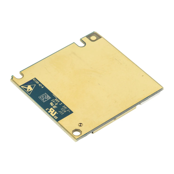
MC75i Hardware Interface Description 6 Mechanics Mechanics Mechanical Dimensions of MC75i Figure 45 shows the top view of MC75i and provides an overview of the board's mechanical dimensions. For further details see Figure Pin80 Pin1 Figure 45: MC75i– top view MC75i_HD_v01.100a... -
Page 103: Figure 46: Dimensions Of Mc75I (All Dimensions In Mm)
MC75i Hardware Interface Description 6.1 Mechanical Dimensions of MC75i Figure 46: Dimensions of MC75i (all dimensions in mm) MC75i_HD_v01.100a Page 103 of 122 2009-08-13 Confidential / Released... -
Page 104: Mounting Mc75I To The Application Platform
6.2 Mounting MC75i to the Application Platform Mounting MC75i to the Application Platform There are many ways to properly install MC75i in the host device. An efficient approach is to mount the MC75i PCB to a frame, plate, rack or chassis. -
Page 105: Board-To-Board Application Connector
Board-to-Board Application Connector This section provides the specifications of the 80-pin board-to-board connector used to connect MC75i to the external application. Connector mounted on the MC75i module: Type: 52991-0808 SlimStack Receptacle 80 pins, 0.50mm pitch, for stacking heights from 3.0 to 4.0mm, see Figure 47 for details. - Page 106 MC75i Hardware Interface Description 6.3 Board-to-Board Application Connector Mating connector types for the customer's application offered by Molex: • 53748-0808 SlimStack Plug, 3mm stacking height, Figure 48 for details. • 53916-0808 SlimStack Plug, 4mm stacking height Note: There is no inverse polarity protection for the board-to-board connector. It is therefore very important that the board-to-board connector is connected correctly to the host application, i.e., pin1 must be connected to pin1, pin2 to pin 2, etc.
-
Page 107: Figure 47: Molex Board-To-Board Connector 52991-0808 On Mc75I
MC75i Hardware Interface Description 6.3 Board-to-Board Application Connector Figure 47: Molex board-to-board connector 52991-0808 on MC75i MC75i_HD_v01.100a Page 107 of 122 2009-08-13 Confidential / Released... -
Page 108: Figure 48: Mating Board-To-Board Connector 53748-0808 On Application
MC75i Hardware Interface Description 6.3 Board-to-Board Application Connector Figure 48: Mating board-to-board connector 53748-0808 on application MC75i_HD_v01.100a Page 108 of 122 2009-08-13 Confidential / Released... -
Page 109: Sample Application
The internal pull-up resistors (Rp) of the I2C interface can be connected to an external power supply or to the VEXT line of MC75i. The advantage of using VEXT is that when the module enters the Power-down mode, the I2CI interface is shut down as well. If you prefer to connect the resistors to an external power supply, take care that the interface is shut down when the PWR_IND signal goes high in Power-down mode. -
Page 110: Figure 49: Mc75I Sample Application
MC75i Hardware Interface Description 7 Sample Application *) I C lines are shared with SPI **) See for details on size of R and FET type for charging circuit. MC75i sample application Figure 49: MC75i_HD_v01.100a Page 110 of 122... -
Page 111: Reference Approval
MC75i Hardware Interface Description 8 Reference Approval Reference Approval Reference Equipment for Type Approval The Cinterion Wireless Modules reference setup submitted to type approve MC75i consists of the following components: • Cinterion Wireless Module MC75i • Development Support Box DSB75 •... -
Page 112: Compliance With Fcc And Ic Rules And Regulations
Manufacturers of mobile or fixed devices incorporating MC75i modules are authorized to use the FCC Grants and Industry Canada Certificates of the MC75i modules for their own final products according to the conditions referenced in these documents. In this case, an FCC/ IC label of the module shall be visible from the outside, or the host device shall bear a second label stating "Contains FCC ID QIPMC75I", and accordingly “Contains IC 7830A-MC75I“. - Page 113 MC75i Hardware Interface Description 8.2 Compliance with FCC and IC Rules and Regulations FCC RF Radiation Exposure Statement "This equipment complies with FCC RF radiation exposure limits set forth for an uncontrolled environment. The antenna used for this transmitter must be installed to provide a separation distance of at least 20 cm from all persons and must not be co-located or operating in conjunc- tion with any other antenna or transmitter."...
-
Page 114: Appendix
Cinterion ordering number: L30960-N1100-A100 Customer IMEI mode: (CS IMEI) Cinterion ordering number: L30960-N1110-A100 DSB75 Evaluation Kit Cinterion Ordering number: L36880-N8811-A100 MC75i mounting clip Please ask Cinterion for ordering details. Votronic Handset VOTRONIC Votronic HH-SI-30.3/V1.1/0 VOTRONIC Entwicklungs- und Produktionsgesellschaft für elektronische Geräte mbH Saarbrücker Str. -
Page 115: Table 42: Molex Sales Contacts (Subject To Change)
MC75i Hardware Interface Description 9.1 List of Parts and Accessories Table 42: Molex sales contacts (subject to change) Molex Molex Deutschland GmbH American Headquarters For further information please click: Felix-Wankel-Str. 11 Lisle, Illinois 60532 http://www.molex.com 4078 Heilbronn-Biberach U.S.A. Germany... -
Page 116: Fasteners And Fixings For Electronic Equipment
MC75i Hardware Interface Description 9.2 Fasteners and Fixings for Electronic Equipment Fasteners and Fixings for Electronic Equipment This section provides a list of suppliers and manufacturers offering fasteners and fixings for electronic equipment and PCB mounting. The content of this section is designed to offer basic guidance to various mounting solutions with no warranty on the accuracy and sufficiency of the information supplied. - Page 117 MC75i Hardware Interface Description 9.2 Fasteners and Fixings for Electronic Equipment Article number: 07.51.403 Insulating Spacer for M2 Self-gripping Length 3.0mm Material Polyamide 6.6 Surface Black Internal diameter 2.2mm External diameter 4.0mm Flammability rating UL94-HB 1. 2 spacers are delivered with DSB75 Support Board Article number: 05.11.209...
- Page 118 MC75i Hardware Interface Description 9.2 Fasteners and Fixings for Electronic Equipment Article number: 01.14.131 Screw M2 DIN 84 - ISO 1207 Length 8.0mm Material Steel 4.8 Surface Zinced A2K Thread Head diameter D = 3.8mm Head height 1.30mm Type Slotted cheese head screw 1.
- Page 119 MC75i Hardware Interface Description 9.2 Fasteners and Fixings for Electronic Equipment Article number: 02.10.011 Hexagon Nut DIN 934 - ISO 4032 Material Steel 4.8 Surface Zinced A2K Thread Wrench size / Ø Thickness / L 1.6mm Type Nut DIN/UNC, DIN934 1.
-
Page 120: Mounting Clip
MC75i Hardware Interface Description 9.3 Mounting Clip Mounting Clip The following figure shows specifications and dimensions for the optional MC75i mounting clip. MC75i_HD_v01.100a Page 120 of 122 2009-08-13 Confidential / Released... -
Page 121: Mounting Advice Sheet
MC75i Hardware Interface Description 9.4 Mounting Advice Sheet Mounting Advice Sheet To prevent mechanical damage, be careful not to force, bend or twist the module. Be sure it is positioned flat against the host device (see also Section 6.2). The advice sheet on the next page shows a number of examples for the kind of bending that may lead to mechanical damage of the module. - Page 122 MC75i Hardware Interface Description 9.4 Mounting Advice Sheet MC75i_HD_v01.100a Page 122 of 122 2009-08-13 Confidential / Released...
Need help?
Do you have a question about the MC75i and is the answer not in the manual?
Questions and answers