Table of Contents
Advertisement
Advertisement
Table of Contents

Subscribe to Our Youtube Channel
Related Manuals for Icom IC-F1610


Summary of Contents for Icom IC-F1610
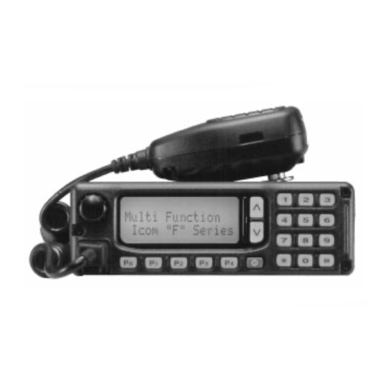
- Page 1 SERVICE MANUAL VHF FM TRANSCEIVER iF1610...
- Page 2 IC-F1610 MAIN UNIT 5 pieces ceiver is defective. 8810008660 Screw BT M3x8 NI-ZU IC-F1610 Bottom cover 10 pieces 6. DO NOT transmit power into a signal generator or a Addresses are provided on the inside back cover for your sweep generator.
-
Page 3: Table Of Contents
TABLE OF CONTENTS SECTION 1 SPECIFICATIONS SECTION 2 INSIDE VIEW SECTION 3 DISASSEMBLY AND OPTION INSTRUCTIONS SECTION 4 CIRCUIT DESCRIPTION 4 - 1 RECEIVER CIRCUITS..........................4 - 1 4 - 2 TRANSMITTER CIRCUITS........................4 - 2 4 - 3 PLL CIRCUITS............................4 - 3 4 - 4 POWER SUPPLY CIRCUITS ........................ - Page 4 SECTION 1 SPECIFICATIONS Mesurement method ETS 300 086 Frequency coverage 146–174 MHz × Number of channels 128 (16 ch 8 banks) 16K0F3E (25 kHz; Wide) Type of emission 8K50F3E (12.5 kHz; Narrow) Operating temperature range –20˚C to +55˚C Power supply voltage 13.2 V DC (negative ground) TX max.
- Page 5 SECTION 2 INSIDE VIEW Low-pass filter circuit MAIN unit Power module* (IC11 : SC-1188) RF amplifier* AF power amplifier (Q1 : 3SK116) (IC8 : LA4425A) 1st IF filter PLL IC* (FI1 : FL-264) (IC12 : MC145190F) Discriminator (X2 : CDBC455CX16) (IC20 : HD64F3437F16) FM IF IC* (IC1 : MC3372SVM)
- Page 6 SECTION 3 DISASSEMBLY AND OPTION INSTRUCTIONS • Opening cover • Installation location Remove 4 screws from bottom cover. Install option units. OPC-617 ACC CABLE: J4 UT-96 5-TONE UNIT or UT-105 SmarTrunk II Logic Board EX-1761 MEMORY EXPANSION UNIT: J7 OPC-822 INTERFACE CABLE: J501 OPC-822 OPC-617 UT-96...
- Page 7 • RMK-1 connection ¡ Remove 3 allen-socket bolts from the front plate using an allen-wrench (1/32 in). ™ Separate the front unit from the transceiver main unit. £ Attach the ‘RMK-1 rear unit attachment’ to the trans- ceiver main unit using the supplied screws. ¢...
-
Page 8: Circuit Description
SECTION 4 CIRCUIT DESCRIPTION 4-1 RECEIVER CIRCUITS through the matching circuit (L15, L52) and a pair of crystal filters (FI1) in order to obtain selection capability and to pass 4-1-1 ANTENNA SWITCHING CIRCUIT only the desired signals. The filtered signal is applied to the The antenna switching circuit functions as a low-pass filter 2nd IF circuit after being amplified at the 1st IF amplifier while receiving and a resonator circuit while transmitting. -
Page 9: Transmitter Circuits
4-1-5 AF AMPLIFIER CIRCUIT A portion of the AF signals from the AF amplifier (IC2) pass through the low-pass filter (Q503) and are then applied to The AF amplifier circuit amplifies the demodulated AF sig- the CTCSS decoder inside the CPU (IC20, pin 43) via the nals to drive a speaker. -
Page 10: Pll Circuits
4-2-2 MODULATION CIRCUIT 4-2-4 APC CIRCUIT The modulation circuit modulates the VCO oscillating signal The APC circuit protects the power module (IC11) from a (RF signal) using the microphone AF signals. mismatched output load and stabilizes the output power. The AF signals from the level controller (IC5) change the The APC detector circuit detects forward signals and reflec- reactance of varactor diodes (D23 and D46) to modulate the tion signals at D3 and D1 respectively. -
Page 11: Power Supply Circuits
4-4 POWER SUPPLY CIRCUIT The lock voltage is also used for the receiver tunable band- pass filters to match the filter’s center frequency to the VOLTAGE LINE desired receive frequency. The lock voltage is amplified at LINE DESCRIPTION the buffer amplifier (Q29) and is then applied to the band- pass filters (D7, D9–D11). -
Page 12: Port Allocations
4-5 PORT ALLOCATIONS CPU (IC20) Port Port Description Description number name number name Outputs the PTT control signal. Outputs strobe signals for the level PTTO DSTB Low : While transmitting controller. (IC5) Input port for the PTT control signal Outputs data signal for the level con- PTTI from PTTO port. -
Page 13: Adjustment Procedures
SECTION 5 ADJUSTMENT PROCEDURES 5-1 PREPARATION REQUIRED TEST EQUIPMENT EQUIPMENT GRADE AND RANGE EQUIPMENT GRADE AND RANGE Output Voltage : 13.2 V DC Frequency range : 0.1–600 MHz DC power supply Standard signal Current capacity : 15 A or more Output level : 0.1 µV –32 mV generator (SSG) -
Page 14: Initial Set Mode
Indicate the received signal level S-METER PC programming. In such case, cannot be used regardless of keys. and only ‘DISPLAY’ setting is available. Ask your Dealer or Icom Service Center for PC programming. Low 1 Low 2 High TX POWER SELECTION METHOD MODE... -
Page 15: Pll Adjustment
5-3 PLL ADJUSTMENT MEASUREMENT ADJUSTMENT ADJUSTMENT ADJUSTMENT CONDITIONS VALUE UNIT LOCATION UNIT ADJUST PLL LOCK • Operating frequency : 136.000 MHz MAIN Connect a digital multi- 3.0 V MAIN VOLTAGE • Receiving meter or an oscillo- scope to the check point, “LV”. -
Page 16: Receiver Adjustment
5-4 RECEIVER ADJUSTMENT ADJUSTMENT MEASUREMENT ADJUSTMENT ADJUSTMENT CONDITIONS METHOD VALUE ADJUST RECEIVER • Operating frequency : 136.000 MHz Number digits in the LCD Maximum indi- Adjust in SENSITIVITY • Connect an SSG to the antenna con- cation sequence nector and set as: L8, L11, L12, L13 Level : 5.6 µV* (–92 dBm) -
Page 17: Transmitter Adjustment
5-5 TRANSMITTER ADJUSTMENT ADJUSTMENT MEASUREMENT ADJUSTMENT ADJUSTMENT CONDITIONS METHOD VALUE ADJUST OUTPUT • Operating frequency : 146.000 MHz Connect an RF power meter to 25 W Rotate volume POWER • Enter Initial Set Mode No. 6. the antenna connector. control while Refer to page 5-2 for details. -
Page 18: Parts List
SECTION 6 PARTS LIST [FRONT UNIT] [FRONT UNIT] ORDER ORDER DESCRIPTION DESCRIPTION 1130009120 S.IC SED1526F0A 7030003680 S.RESISTOR ERJ3GEYJ 104 V (100 kΩ) 1140007630 S.IC HD64F3644H 7030003680 S.RESISTOR ERJ3GEYJ 104 V (100 kΩ) 1110003500 S.IC S-80742SL-A6-T1 7030003680 S.RESISTOR ERJ3GEYJ 104 V (100 kΩ) 1130005720 S.IC TC7W04F (TE12L) 7030003680 S.RESISTOR... - Page 19 [FRONT UNIT] [MAIN UNIT] ORDER ORDER DESCRIPTION DESCRIPTION DS11 5040002030 S.LED CL-170Y-CD-T 1590002290 S.TRANSISTOR FMS2A T148 DS13 5040002030 S.LED CL-170Y-CD-T 1590002300 S.TRANSISTOR FMW2 T148 DS14 5040002030 S.LED CL-170Y-CD-T 1530002060 S.TRANSISTOR 2SC4081 T107 R DS15 5040002030 S.LED CL-170Y-CD-T 1510000510 S.TRANSISTOR 2SA1576A T106R DS16 5040002030 S.LED CL-170Y-CD-T 1530002060 S.TRANSISTOR...
- Page 20 [MAIN UNIT] [MAIN UNIT] ORDER ORDER DESCRIPTION DESCRIPTION ERJ3GEYJ 470 V (47 Ω) 1750000260 S.DIODE 1SS352 (TPH3) 7030003280 S.RESISTOR ERJ3GEYJ 1R0 V (1 Ω) D501 1160000060 S.DIODE DAN202U T107 7030004050 S.RESISTOR ERJ3GEYJ 470 V (47 Ω) D502 1160000060 S.DIODE DAN202U T107 7030003280 S.RESISTOR ERJ3GEYJ 1R0 V (1 Ω) D503...
- Page 21 [MAIN UNIT] [MAIN UNIT] ORDER ORDER DESCRIPTION DESCRIPTION ERJ3GEYJ 151 V (150 Ω) R116 7030003340 S.RESISTOR R240 7030003660 S.RESISTOR ERJ3GEYJ 683 V (68 kΩ) R117 7030003470 S.RESISTOR ERJ3GEYJ 182 V (1.8 kΩ) R242 7030003500 S.RESISTOR ERJ3GEYJ 332 V (3.3 kΩ) ERJ3GEYJ 471 V (470 Ω) R118 7030003400 S.RESISTOR...
- Page 22 [MAIN UNIT] [MAIN UNIT] ORDER ORDER DESCRIPTION DESCRIPTION R342 7030003660 S.RESISTOR ERJ3GEYJ 683 V (68 kΩ) R534 7030003800 S.RESISTOR ERJ3GEYJ 105 V (1 MΩ) R344 7030003560 S.RESISTOR ERJ3GEYJ 103 V (10 kΩ) R535 7410000950 S.ARRAY EXB-V8V 102JV R348 7030003510 S.RESISTOR ERJ3GEYJ 392 V (3.9 kΩ) R538 7410000950 S.ARRAY...
- Page 23 [MAIN UNIT] [MAIN UNIT] ORDER ORDER DESCRIPTION DESCRIPTION 4030011770 S.CERAMIC C1608 CH 1H 060B-T-A C127 4030007060 S.CERAMIC C1608 CH 1H 270J-T-A 4030006860 S.CERAMIC C1608 JB 1H 102K-T-A C128 4030007020 S.CERAMIC C1608 CH 1H 120J-T-A 4030006850 S.CERAMIC C1608 JB 1H 471K-T-A C129 4030007070 S.CERAMIC C1608 CH 1H 330J-T-A...
- Page 24 [MAIN UNIT] [MAIN UNIT] ORDER ORDER DESCRIPTION DESCRIPTION C229 4030011600 S.CERAMIC C1608 JB 1C 104KT-N C341 4030006860 S.CERAMIC C1608 JB 1H 102K-T-A C230 4550002890 S.TANTALUM TESVA 1A 225M1-8L C343 4030006860 S.CERAMIC C1608 JB 1H 102K-T-A C231 4030006860 S.CERAMIC C1608 JB 1H 102K-T-A C344 4030006860 S.CERAMIC C1608 JB 1H 102K-T-A...
- Page 25 [MAIN UNIT] [TONE UNIT] ORDER ORDER DESCRIPTION DESCRIPTION C517 4030011600 S.CERAMIC C1608 JB 1C 104KT-N 0880000150 UNIT BOARD UT-96 [EUR-11] only C518 4550006250 S.TANTALUM TEMSVA 1A 106M-8L C519 4550006250 S.TANTALUM TEMSVA 1A 106M-8L C520 4030008630 S.CERAMIC C1608 JF 1C 104Z-T-A C521 4550006250 S.TANTALUM TEMSVA 1A 106M-8L...
- Page 26 SECTION 7 MECHANICAL PARTS [CHASSIS PARTS] [UNPACKING] REF. NO. ORDER NO. DESCRIPTION QTY. REF. NO. ORDER NO. DESCRIPTION QTY. 6510004880 Connector MR-DS-E 01 5210000120 Fuse FGB 15A Optional product Microphone HM-100 8010016320 1705 chassis 8810008660 Screw PH BT M3 x 8 NI-ZU Optional product Speaker SP-22 8810008660...
- Page 27 OPPOSITE DIRECTION TO THE MAIN UNIT MP4(C) J1(C) MP8(M) W4(M) MP2(C) MP2(C) MP12(M) FRONT UNIT MP9(F) R26(F) MP9(M) J1(F) MP1(C) MAIN (Top side) MP11(C) MP2(M) + MP4(M) J5(M) MP6(M) MP4(F) MP3(F) MP16(C) MP13(M) EP2(F) MP12(C) MP11(M) DS1(F) MP15(C) MP7(M) MP2(F) J2(M) MAIN UNIT (Bottom side) MP10(M)
-
Page 28: Semi-Conductor Information
SECTION 8 SEMI-CONDUCTOR INFORMATION • TRANSISTORS AND FET’S • DIODES 2SA1576 2SB1123T 2SC4081 R 2SC4116 BL 2SC4215 O 1SS352 1SS355 1SS375 1SV214 1SV217 (Symbol: FR) (Symbol: BF) (Symbol: BR) (Symbol: LL) (Symbol: QO) (Symbol: C1) (Symbol: A) (Symbol: FH) (Symbol: T1) (Symbol: T6) 2SC4226 R25 2SC4703 SE... -
Page 29: Board Layouts
SECTION 9 BOARD LAYOUTS 9-1 FRONT UNIT The combination of this page and the next page show the • TOP VIEW unit layout in the same config- uration as the actual P. C. Board. HANG MICE CLON 9 - 1... - Page 30 • BOTTOM VIEW FTXD FRXD POSW MICE from MAIN unit J5 9 - 2...
-
Page 31: Main Unit
9-2 MAIN UNIT The combination of this page and the next page show the unit layout in the same configuration as the actual P. C. Board. CHASSIS MP12 • TOP VIEW BLACK IC11 MT8V TMUT MP9, MP8 J501 L.V. OPS1 OPS2 from Optional cable... - Page 32 MP12 • BOTTOM VIEW MP13 MP10 MP11 9 - 4...
-
Page 33: Block Diagram
SECTION 10 BLOCK DIAGRAM 136-174 MHz DISC UM9401F AF OUT SFPC455H TX/RX M5282FP TA75W558FU D501 D502 3SK166 DAN202U DAN202U 3SK166 FL-264 EXT SP DTC114EU Q501,Q502,Q510 DTC144EU MUTE CTRL FM IC +20V Q61 2SC4116 LA4425A 2SC4215 2SC5110 DTC363EK 2SC4116 AMUT TUNE MC3372SVM MT8V MT8V... -
Page 34: Voltage Diagram
SECTION 11 VOLTAGE DIAGRAM 11-1 FRONT UNIT LIGHT ON (DIM OFF) 7.64V LIGHT ON (DIM OFF) 7.75V LIGHT ON (DIM ON) 5.99V LIGHT ON (DIM ON) 6.20V LIGHT ON LIGHT OFF LIGHT OFF 7.98V LIGHT OFF 7.98V 5.04V 100k 100k 100k 100k 100K... -
Page 35: Main Unit
11-2 MAIN UNIT PAMIC 1/2VDD DATA BUS PAAF W508 R162 C354 C344 0.001 0.001 PSET PSET C184 +18V +18V 0.001 5.04V R298 R348 C563 C362 R148 R319 R304 0.56 R374 PLLIN 7.00V 8.02V 3.9k 0.001 R239 C307 100k R303 C155 C557 2SC4081 0.56... - Page 36 OPT AF BUS AF BUS 4.81V SQL OPEN 4.88V SQL CLOSE 0V R62 1.5k 0.047 0.047 0.047 SQL OPEN 0.89V 2.2k SQL OPEN 0V W508 R338 SQL CLOSE 4.60V 4.00V SQL CLOSE 4.26V R595 2.52V 2.54V 2.54V 0.047 R357 PSET PSET 4.12V 2.7k...
- Page 37 11-2 MAIN UNIT OPT AF BUS AF BUS 4.81V PAMIC 1/2VDD SQL OPEN 4.88V PAAF DATA BUS SQL CLOSE 0V SQL OPEN 0.89V R62 1.5k 0.047 2.2k 0.047 0.047 W508 R338 SQL OPEN 0V SQL CLOSE 4.60V 4.00V R162 SQL CLOSE 4.26V R595 2.52V C354...
- Page 38 08190 Sant Cugat Del Valles Barcelona, SPAIN Phone : ( 93 ) 589 46 82 Fax : ( 93 ) 589 04 46 A Division of Icom America Inc. E-mail : icom@lleida.com 3071 #5 Road, Unit 9, Richmond, B.C., V6X 2T4, Canada...
- Page 39 A-5547HI-SV 6-9-16, Kamihigashi, Hirano-ku Osaka 547-0002, Japan C 1998 by Icom Inc.
Need help?
Do you have a question about the IC-F1610 and is the answer not in the manual?
Questions and answers