Table of Contents
Advertisement
Quick Links
Advertisement
Table of Contents

Related Manuals for Microsemi VSC8502


Summary of Contents for Microsemi VSC8502
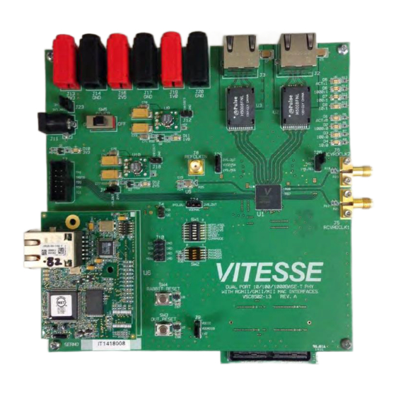
- Page 1 VSC8502 User Guide VSC8502 Evaluation Board January 2019...
-
Page 2: Table Of Contents
Driving Recovered Clock Output ......................11 4.4 Useful Test Features ......................... 11 4.4.1 Ethernet Packet Generator ........................11 4.4.2 Copper PHY Error Counters ........................11 4.4.3 Near-End Loopback ..........................11 4.4.4 Far-End Loopback ..........................12 VPPD-03741 VSC8502 User Guide Revision 1.1... -
Page 3: Revision History
Revision 1.1 of this datasheet was published in January 2019. The new Microchip template was added to the document. Revision 1.0 Revision 1.0 of this datasheet was published in May 2014. This was the first publication of the document. VPPD-03741 VSC8502 User Guide Revision 1.1... -
Page 4: Introduction
Wake-on-LAN (WOL) power management using magic packets. This document describes the architecture and usage of the VSC8502 Evaluation Board (VSC8502EV). The Quick Start section describes how to install and run the graphical user interface (GUI) to fully control the evaluation board. - Page 5 VSC8502 Evaluation Board Figure 2 • VSC8514 Evaluation Board (Bottom View) Additional VSC8502 collateral for both the VSC8502 device and VSC8502EV, including schematics, layout, GUI, and application notes can be found on the VSC8502 product web page at: https://www.vitesse.com/products/product.php?number=VSC8502 VPPD-03741 VSC8502 User Guide Revision 1.1...
-
Page 6: General Description
VSC8502 Evaluation Board General Description The evaluation board, shown in Figure 1, provides the user a way to evaluate the VSC8502 device in multiple configurations. Two RJ-45 connectors are provided for copper media interfaces. The MAC interface is exposed via SAMTEC connector (J1) that allows for the complete eval board to be mated with a motherboard having the necessary signals for operating the device. - Page 7 Note: R17 and R18 0 ohm options must be installed for PHYADD1 and PHYADD2 to be affected by SW2, otherwise they are internally pulled to GND. Also, PHYADD3-4 pins are internal PD on the VSC8502 IC, and are weakly pulled to GND when their corresponding SW2 pins are kept in ‘0’ position.
-
Page 8: External Refclk Option
Figure 5 • REFCLK Input Options - R25 3-Way Orientation 3.1.3 Recovered Clocks There are two recovered clocks available from the VSC8502, through SMA connections J5 (RCVRDCLK1) and J6 (RCVRDCLK2). In the default configuration, CLK_SQUELCH_IN is pulled down, which disables the clock squelching and RCVRDCLK1/RCVRDCLK2 are connected to the Samtech header J1. -
Page 9: Gmii Loopback Card
However, there are other internal loopback modes that will support BER testing of MII mode such as far- end loopback (MII Register 23.3). Key Features This section shows the power supply options for VSC8502. VPPD-03741 VSC8502 User Guide Revision 1.1... -
Page 10: Single 3.3 V Input For Both Dut And Other Components
DUT On-chip Regulator Power The on-chip regulator option for this board is for engineering purposes only. There are performance issues associated with using the on-chip regulator on this board, so it is an unsupported board feature. VPPD-03741 VSC8502 User Guide Revision 1.1... -
Page 11: Quick Start
VSC8502 Evaluation Board Quick Start This section shows the quick start for VSC8502. Connecting the Power Supply The evaluation board offers choices of how to power the 3.3 V, 2.5 V, and 1.0 V rails which drive the devices as well as modules; please see section 2.2 for reference. The simplest power option for the evaluation board is to use the power pack for 3.3 VDC. -
Page 12: Board Initialization
0, 4 and 9 to change speed and restart autoneg (MII 0 bit 9) to advertise new settings. As per the datasheet descriptions, the commonly-used speed advertisement definitions are as follows: Table 3 • Auto-Negotiation Advertisements VPPD-03741 VSC8502 User Guide Revision 1.1... -
Page 13: Driving Recovered Clock Output
To enable the loopback, set register bit 0.14 to 1. Near-end loopback mode involves traffic flow over the GMII/RGMII interface, so a breakout of the MAC interface on SAMTEC connector J1 must be connected to another system for this mode to pass traffic. VPPD-03741 VSC8502 User Guide Revision 1.1... -
Page 14: Far-End Loopback
When the far-end loopback test feature is enabled, incoming data from a link partner on the Copper interface to be transmitted back to the link partner on the Copper interface. To enable the loopback, set register bit 23.3 to 1. VPPD-03741 VSC8502 User Guide Revision 1.1... - Page 15 Microsemi. It is the Buyer's responsibility to independently determine suitability of any products and to test and verify the same. The information provided by Microsemi hereunder is provided "as is, where is" and with all faults, and the entire risk associated with such information is entirely with the Buyer.
Need help?
Do you have a question about the VSC8502 and is the answer not in the manual?
Questions and answers