Table of Contents
Advertisement
®
®
Bose
Lifestyle
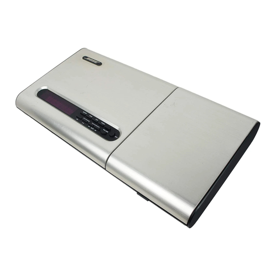
Model CD5 Series I Music Center
Note: The first series CD5 can be distinguished from the later CD5V and CD5VII by the serial
number label located on the bottom of the unit. The CD5 will not have a V on the serial number
label, the CD5V will have a V, and the CD5V2 will have a V with the number 2 above the V.
©
1998 Bose Corporation
Service Manual
Part Number 174798 REV 01
Advertisement
Table of Contents

Related Manuals for Bose Life CD5 Series I


Summary of Contents for Bose Life CD5 Series I
- Page 1 The CD5 will not have a V on the serial number label, the CD5V will have a V, and the CD5V2 will have a V with the number 2 above the V. © 1998 Bose Corporation Service Manual Part Number 174798 REV 01...
-
Page 2: Table Of Contents
® BOSE CORPORATION WHICH IS BEING FURNISHED ONLY FOR THE PURPOSE OF SERVICING THE IDENTIFIED BOSE PRODUCT BY AN AUTHORIZED BOSE SERVICE CENTER OR OWNER OF THE BOSE PRODUCT, AND SHALL NOT BE REPRODUCED OR USED FOR ANY OTHER PURPOSE. -
Page 3: Safety Information
SAFETY INFORMATION 1. Parts that have special safety characteristics are identified by the symbol on schematics or by special notes in the part lists. Use only replacement parts that have critical characteristics recommended by the manufacturer. 2. Make leakage current or resistance measurements to determine that exposed parts are acceptably insulated from the supply circuit before returning the unit to the customer. -
Page 4: Specifications
SPECIFICATIONS General Dimensions: 2.5"H x 15"W x 9"D (6 x 38 x 23cm) Weight: 3.7lb. (1.7kg) Finish: Plastic, in-mold brushed aluminum finish Power Input: Detachable power pack, 12VAC compatible with each country's power requirements Serial Data Output: 2-3.5mm stereo jacks, Tip: Serial data output, Ring: +12Vdc turn on output. -
Page 5: Specifications
SPECIFICATIONS (Continued) AM Electrical Antenna Input: Binding posts Usable Sensitivity: 55dBuV/m (IHF standard test loop antenna) Alternate Channel Selectivity: 60dB Adjacent Channel Selectivity: 45dB Image Rejection Ratio: 40dB S/N Ratio: 50dB (@ 100dBuV/m) ≤ 1.0% (@ 100dBuV/m) THD: Frequency Response (@ 100dBuV/m): 100Hz: -8dB 3kHz: -8dB CD Electrical... -
Page 6: Figure 1. Cd5 Block Diagram Sheet 1 Of 2
Figure 1. CD5 Block Diagram Sheet 1 of 2... -
Page 7: Figure 2. Cd5 Block Diagram Sheet 2 Of 2
Figure 2. CD5 Block Diagram Sheet 2 of 2... -
Page 8: Cd Terms
CD TERMS Basic Terms Access: See track access. Access Time: The length of time required to change tracks. CD Mechanism: The mechanical assembly of components used to read information off of the CD. It contains the optical pickup, sled assembly, disc motor, sled motor, and spindle. Disc Motor: The motor which spins the disc. - Page 9 CD TERMS Eccentricity: The extent to which the hole in the middle of the disc is not located in the geo- metric center. In other words, the amount that the disc moves in and out as it rotates. Eccen- tricity is measured as the distance between the center of the hole and the center of the disc (as determined by the spiral tracks).
- Page 10 CD TERMS Tracking Gain: The overall loop gain of the tracking servo. This controls how tightly the laser is held in the center of the track. If the gain is too low, the player will have trouble with vibration and eccentric discs, especially during track access. If the gain is too high the player will have skips or mistracking with voids and scratches.
- Page 11 CD TERMS Major Components of the System ASP: Analog Signal Processor. The component in the CD circuitry that contains the RF ampli- fier, VCO, and the tracking, focus, and sled servos. DSP: Digital Signal Processor. The component in the CD circuitry that performs slicing, EFM demodulation, CIRC decoding, error correction and concealment, track access, CLV regula- tion, and drives the D/A.
-
Page 12: Cd Terms
CD TERMS Signal Names (continued) TAP: Test Access Port. A 3 pin test interface used by automated test to control and observe the board under test. TDO: Tracking Drive Output. TEAO: Tracking Error Amplifier Output. TGL: Tracking Gain Low. THLD: Tracking Hold. TOFF: Tracking Off TPA+: Tracking Pre-Amplifier (+ input). -
Page 13: Theory Of Operation
Model 5 music center is a self-contained CD player, AM/FM tuner, preamplifier, ® and control center for use with Bose powered speaker systems. In addition to the two internal sources (CD and tuner), it also allows for up to three external devices to be connected (i.e. - Page 14 THEORY OF OPERATION There is one main serial data bus that controls source selection IC U101, volume control IC U103, PLL frequency synthesizer U302, and EEPROM U401. The clock and data information for all of these devices is sent out on U402, pins 5 and 7. However, U401, U302, U101 and U103 each have their own chip select line.
- Page 15 THEORY OF OPERATION U103’s output signal is buffered by U105, and is fed to the A and B outputs. These outputs are independently mutable through transistors Q103-106 and Q203-206. Each pair of transistors provides approximately 80dB of attenuation when muted. These mute transistors are con- trolled by the signals on J9-7 and J9-8.
- Page 16 THEORY OF OPERATION The E and F signals are amplified and subtracted. This produces the tracking error signal TEAO (U501, pin 7 ). The F channel’s gain is adjusted by E-F balance potentiometer R506. The TEAO signal is used by the anti-shock circuit, the track jump detection circuit, and the tracking servo.
- Page 17 THEORY OF OPERATION U505’s oscillator is obtained from a 4MHz ceramic resonator (X502). U505 is reset by a rising edge on pin 1 that is caused by R573 and C574. This occurs automatically on power-up, but may be forced manually by depressing S502 (if installed). U505 communicates with U502 on a serial bus (U502, pins 50 through 54).
-
Page 18: Theory Of Operation
THEORY OF OPERATION oscillator tuned circuit. The tuned output appears on pin 12 and is fed to AM buffer FET Q300. The buffered output is sent to U301, pin 27. U301 contains the AM RF amplifier, mixer, IF amplifier, AM detector and AM stop level detection. Potentiometer R339, which is connected to pin 16, sets the AM stop level to 70dB uV/M (nominal). -
Page 19: Figure 3. Labelled Exploded View
See Figure 6 for a side view of this assembly. Figure 3. Labelled Exploded View... -
Page 20: Disassembly/Assembly Procedures
DISASSEMBLY/ ASSEMBLY PROCEDURES 1. Left Cover Assembly Removal front of the base assembly (19). Lower the Note: Refer to Figures 3 and 5 for Proce- cover into position. dures 1 and 2. 4.3 There are two black tabs on the bottom 1.1 Remove the two screws (18A) that of the right cover. - Page 21 DISASSEMBLY/ ASSEMBLY PROCEDURES 5.5 Slide the violet (14) and gray (15) 7.1 Remove the left cover assembly (Pro- grommets away from the slots in each cedure 1) and the right cover/door assem- corner of the mechanism. bly (Procedure 3). 5.6 Remove the two screws (13) that 7.2 Lift up the CD mechanism (11) and secure the cover (12) to the mechanism.
-
Page 22: Disassembly/Assembly Procedures
DISASSEMBLY/ASSEMBLY PROCEDURES 9.3 Slide the PCB clear of the connector 12. Headphone Jack PCB Replacement panel, and pull it away from the base. 12.1 Snap the PCB (10) into place by 9.4 Remove any connections required to engaging the two locking tabs. troubleshoot the PCB. -
Page 23: Figure 5. Back Panel With Tab Locations
Figure 5. Back Panel with Tab Locations Hooks onto front of console. Tab that fits into cutouts on back panel Figure 6. Right Cover Assembly (side view) Figure 7. Base Assembly (top view with covers removed) -
Page 24: Rc5 Disassembly/Assembly Procedures
RC5 DISASSEMBLY/ASSEMBLY PROCEDURES 1. Enclosure Disassembly 2.2 Press the top cover and the bottom cover together until they snap into place. 1.1 Slide off the battery compartment door (5) and remove the batteries. 3. PCB Removal 1.2 While holding the top cover (4) with one 3.1 Lift the PCB (1) straight up. -
Page 25: Test Procedures
TEST PROCEDURES GENERAL TEST SETUP 2.4 Measure the outputs according to the following table. Load the outputs as follows: Output Separation (dB) Headphone output-33Ω, 1% load. ≥50 Speaker A (L,R) Audio (A, B, Fixed) outputs-10kΩ load. ≥50 Speaker B (L,R) ≥50 Tape (L,R) Note: The remote control or console... - Page 26 TEST PROCEDURES 5. Headphone Mute 3.3 Adjust the generator's output to 35dBf. Verify that U301 pin 21 is < 2.5Vdc. 5.1 Select the AUX input. 4. Stereo Separation 5.2 Apply a 500mVrms, 1kHz signal to the L/R AUX input. 4.1 Set the RF generator to 65 dBf, pilot on, left modulation, 1kHz, 100% (75kHz devia- 5.3 Insert a mini-jack into the headphone tion).
-
Page 27: Test Procedures
TEST PROCEDURES AM ALIGNMENT PROCEDURES 1.2 Reference a dB meter to the Fixed level output. Test setup: Connect the generator to a standard radiating loop. Unless otherwise 1.3 Shut off the modulation and measure noted, set an RF generator to 70dBu field the noise. -
Page 28: Cd Test Procedures
Digital Voltmeter 2.6 Adjust R511 until the meter reads Frequency Counter between -7 to 17mVdc. Sony Disc YEDS-18 Bose ® CD Alignment Fixture (176318) 3. E/F Balance (E/F) 1. PLL Free Run Frequency (VCO) 3.1 Advance the alignment fixture (ADV... -
Page 29: Figure 11. Cd Alignment Fixture And Test Setup
CD TEST PROCEDURES 5. Focus Gain (FG) 5.1 Advance the fixture to FG and set the voltmeter to read AC voltage. 5.2 Simulate a closed CD door by placing an object between S501's two black posts (the CD door latch can be used). Load the test disc, select CD (S413), and play track 5.3 Adjust R527 until the meter reads between 380 to 420mVrms. -
Page 30: Figure 12. Passive Filter Network And Test Setup
Figure 12. Passive Filter Network and Test Setup... - Page 31 CD TEST PROCEDURES CD ALIGNMENT PROCEDURES 3. E/F Balance Note: The test disc is required for this test. (Without Fixture) Construct the filter indicated in Figure 12 and connect it to P504 pin 4 (TEAO). Note: Refer to Figure 12 throughout this procedure.
- Page 32 CD TEST PROCEDURES 5.3 Skip back to the beginning of track 2. 3.4 Fingerprint: Play track 15 (75µm). Listen for at least 10 seconds. 5.4 Adjust R527 until the meter reads between 23.2 ± 1.5mVrms. 6. Tracking Offset Readjustment 6.1 Refer to procedure 2 and readjust if necessary.
-
Page 33: Figure 13. Digital Pcb Adjustment Locations
Figure 13. Digital PCB Adjustment Locations... -
Page 34: Parts List Notes
PARTS LIST NOTES 1. This part is not normally available from Customer Service. Approval from the Field Service Manager is required before ordering. 2. The individual parts located on the PCBs are listed in the Electrical Parts List. This part is critical for safety purposes. Failure to use a substitute replacement with the same safety characteristics as the recommended replacement part might create shock, fire and/or other hazards. -
Page 35: Console Assembly Parts List
CONSOLE ASSEMBLY PARTS LIST (Figure 14) Item Description Part Number Note Number Door Assembly 187743-001 Spring-Torsion, LH 176083 Spring-Torsion, RH 176082 Pin-Hinge, 5.3" 173210 Gear-Damper, Blue 146816-05 Cover Assembly, Right 149956 Cover Assembly, Left 190819 Nameplate, Flat Black 180213 Spring, Ground 173449 PCB Assembly, 120V 146075-101A... -
Page 36: Figure 14. Exploded View
Figure 14. Exploded View... -
Page 37: Remote Control Assembly Parts List
REMOTE CONTROL ASSEMBLY PARTS LIST (Figure 15) Item Description Part Number Note Number PCB ASSY RMT CNTRL, RC-5A 194387 1, 2 MAT, SWITCH, CD-5 146088 COVER, BOTTOM, CD-5 146089 COVER, TOP, CD-5 146090 DOOR, BATTERY, CD-5 146226 CONTACT, BATTERY, CONE 174001 CONTACT, BATTERY, FLAT 174000... -
Page 38: Electrical Part List
ELECTRICAL PART LIST Resistors Reference Description Part Number Reference Designator R1, 4, 113, 213, 1kΩ, 5%, 1/10W, 133626-1025 US/Can. 330, 333, 336, 342, 0805 348, 353, 145, 406, 420-423, 426, 427, 431, 433-442, 502, 503, 553, 572, 598, R2, 315 133625-5111 5.11kΩ, 1%, 1/10 0805... - Page 39 ELECTRICAL PART LIST Resistors (Continued) Reference Description Part Number Note Designator R121, 128, 221, 228 432Ω, 1%, 1/10W, 133625-4320 0805 R122, 129, 222, 229 182Ω, 1%, 1/10W, 133625-1820 0805 R126, 226 150Ω, 1%, 1/10W, 133625-1500 0805 R134-136, 142, 599, 1MΩ, 5%, 1/10W, 133626-1055 0805 R138, 304, 309,...
- Page 40 ELECTRICAL PART LIST Resistors (Continued) Reference Description Part Number Note Designator R339, 558 Potentiometer, 20kΩ, 170042-203 10%, 1/2W R340 120Ω, 5%, 1/10W, 133626-1215 0805 R343, 501 10Ω, 5%, 1/10W, 133626-1005 0805 R344, 346, 349, 330Ω, 5%, 1/10W, 133626-3315 351, 429, 430, 561, 0805 R347, 352 18kΩ, 5%, 1/10W,...
- Page 41 ELECTRICAL PART LIST Resistors (Continued) Reference Description Part Number Note Designator R537 160kΩ, 5%, 1/10W, 133626-1645 0805 R541 133626-9135 91kΩ, 5%, 1/10 0805 R567 133626-2045 200kΩ, 5%, 1/10 0805 R570 133626-6835 68kΩ, 5%, 1/10 0805 R573, 579 270kΩ, 5%, 1/10W, 133626-2745 0805 R586, 587, 590, 591 2.21kΩ, 1%, 1/10...
- Page 42 ELECTRICAL PART LIST Capacitors (continued) Reference Description Part Number Note Designator C110, 210, 302, 4.7µF, 20%, 50V, 149948-4R7H 305, 342 85, EL C113, 213, 301, 47µF, 20%, 25V, 149948-470E 324, 331, 346 85, EL C115, 215 22µF, 20%, 25V, 149948-220E 85, EL C121, 130, 133, .01µF, 10%, 50V,...
- Page 43 ELECTRICAL PART LIST Capacitors (continued) Reference Description Part Number Note Designator C507 560pF, 5%, 50V, 133622-561 COG, 0805 C508 1µF, 20%, 50V, 147522-1R0 EL, 85, BP C509 .018µF, 5%, 100V, 137127-183 85, Box C510 .47µF, 20%, 50V, 147522-R47 EL, 85, BP C511, 514, 525, .033µF, 5%, 63V, 137127-333...
- Page 44 ELECTRICAL PART LIST Diodes (continued) Reference Description Part Number Note Designator D407 Zener, 1N5232, 136758-5232 5.6V, .5W, 5% D504 Zener, 1N5231, 136758-5231 5.1V, .5W, 5% D505 Zener, 1N4742A, 116995-4742A 12V, 1W, 5% Transistors Reference Description Part Number Note Designator Bipolar, P, 60V, 147529-S 5A, TO-126 Q101-107, 201-207...
- Page 45 ELECTRICAL PART LIST Integrated Circuits (continued) Reference Description Part Number Note Designator U401 EEPROM, 147536 59C11, 1 KB, SO-8 U402 Microcontroller, 178324 68HC05C12, Programmed U403 VFD Driver, 146813 MM58342, DIP28 U501 ASP, LA9210M, 146809 DIP80 U502 DSP, LC7867, 146810 DIP64 U503, 504 Motor Driver, 146808...
- Page 46 ELECTRICAL PART LIST Crystals Reference Description Part Number Note Designator X301 Crystal, Quartz, 147223 7.2MHz, 50 PPM X401, 502 Resonator, 147534 Ceramic, 4MHz X501 Crystal, 147533 16.93444MHz, 100 Tuning Coils Reference Description Part Number Note Designator T301, 302 Filter, Stereo MPX, 147236 Single-tuned T303...
-
Page 47: Electrical Part List
ELECTRICAL PART LIST Miscellaneous (continued) Reference Description Part Number Note Designator J101, 102 Connector, Jack, 149959 Quad Phono J103 Connector, Jack, 148766 Phono, 6 pos. J104 Connector, Jack, 148583 Headphone, 3.5mm J105A-B, 105B-A Cable, 26 AWG, 148771-0513 5 conductor, 2 mm, 13" J301 Connector, 148586... -
Page 48: Rc5 Electrical Part List
RC5 ELECTRICAL PART LIST Resistors Reference Description Part Number Note Designator R2-5,13, 21-23 200kΩ, 5%, 1/10W, 133626-2045 0805 R6, 9 100kΩ, 5%, 1/10W, 133626-1045 0805 470kΩ, 5%, 1/10W, 133626-4745 0805 4.7kΩ, 5%, 1/10W, 133626-4725 0805 2.7kΩ, 5%, 1/10W, 133626-2725 0805 1kΩ, 5%, 1/10W, 133626-1025 0805... - Page 49 RC5 ELECTRICAL PARTS LIST Capacitors (continued) Reference Description Part Number Note Designator 33pF, 5%, 50V, 133622-330 COG, 0805 27pF, 5%, 50V, 133622-270 COG, 0805 56pF, 5%, 50V, 133622-560 COG, 0805 22pF, 5%, 50V, 133622-220 COG, 0805 39pF, 5%, 50V, 133622-390 COG, 0805 68pF, 5%, 50V, 133622-680...
-
Page 50: Rc5 Electrical Part List
RC5 ELECTRICAL PARTS LIST Miscellaneous Reference Description Part Number Note Designator Connector 171982 receptacle, Battery contact (2 in qty.) L2, 5, 6, 9 10µH, 160A, 147563-100 7.96Hz, Axial 6.8µH, 175A, 147563-6R8 7.96Hz, Axial 1.2µH, 260A, 147563-1R2 7.96Hz, Axial .47µH, 330A, 147563-R47 25.2Hz, Axial Bar antenna,... -
Page 51: Packaging Part List
PACKAGING PART LIST Item Description Part Number Note Number Remote Control Assembly (RC5A) 179980 Remote Control Assy Packaged for Resale 172724 Polybag (Remote) 144348 Wire Cover 173201 Power Supply, 120V (US/Can.) 146225 Power Supply, 220V (Eur.) 146798 Power Supply, 230V (UK/Sing.) 146799 Power Supply, 240V (Aus.) 146800... - Page 52 (See diagrams below) Note: Latter production units used an improved reset circuit (U404). U404 is located on the display PCB under the BOSE ® logo. This modification is not needed on these units.
- Page 53 # 177871-B1 Product: CD-5 Subject: Display Failure Symptom: Flashing VFD displays are being observed on CD-5 units. Reason: The existing ground trace breaks at the pad leaving no ground. This change affects PCB P/N 177400 and has been added to all production units starting the week of 12/17/95.
- Page 54 174798-B1 ® Product: Lifestyle Subject: Dim VFD Display Effective Date: 8/27/96 Symptom: Dim VFD Display. Reason: Improper voltage rating on C19. Solution: Replace C19 with a 33uF, 63V capacitor, part number 149948-3301J. The display dims on some units, after the unit has been in use for a period of time. When a unit is returned from the field for service, C19 should be checked to ensure that the voltage rating on C19 is 63V.
-
Page 55: Service Bulletin
CD5 TROUBLESHOOTING GUIDE Symptom Probable Cause Solution Service Bulletin C2, physical damage Replace C2 Intermittent or no operation P1, fractured solder joint or Repair fractured solder joint lifted pad or lifted pad. No operation Q2, 3, 4, 5 failed Replace Q2, 3, 4, 5. Display Dim C19 voltage under rated Replace C19 with a 33uF,... -
Page 56: Cd5 Voltages And Waveforms
CD5 VOLTAGES AND WAVEFORMS Remote Control Voltages Node Voltages Units Test Condition Min. Typical Max. Q1 C 4.50 Button pressed Q1 C 0.00 Remote off Q3 C 0.00 Remote off Q4 B 1.25 Button pressed Q4 E Button pressed Power Supply Section Voltages (Reference Designators 0-99) Node Voltages Units... - Page 57 CD5 VOLTAGES AND WAVEFORMS Microcontroller Section Voltages (Reference Designators 400-499) Node Voltages Units Test Condition Min. Typical Max. U402 Pin 40 (Vdd) U402 Pin 35 (reset) U402 Pin 36 Tuner Section Voltages (Reference Designators 300-399) Node Voltages Units Test Condition Min.
- Page 58 CD5 VOLTAGES AND WAVEFORMS CD Section Voltages (Reference Designators 500-699) Node Voltages Units Test Condition Min. Typical Max. U501 pin 80 (Vref1) CD on U501 pin 8 (Vref2) CD on U501 pin 9 (Vref3) CD on U501 pin 7 (TEAO) CD on U501 pin 15 (TPAO) CD on...
- Page 59 CD5 VOLTAGES AND WAVEFORMS Power Supply Section Waveforms (Reference Designators 0-99) Node Waveform Bias Level Amplitude Frequency Test Condition (VDC) C18- Sine -15.3 4.3 VPP 50/60HZ Display off C19- Sine -15.3 1.3 VPP 50/60HZ Display off Microcontroller Section Waveforms (Reference Designators 400-499) Node Waveform Bias Level...
-
Page 60: Integrated Circuit Diagrams
INTEGRATED CIRCUIT DIAGRAMS Remote Transmitter U101 Analog Switch TC9163N U103 Volume Control TC9213P... - Page 61 INTEGRATED CIRCUIT DIAGRAMS Monostable Multivibrator CD4538 U301 AM/FM Tuner LA1851N U302 PLL Frequency Synthesizer LM7000...
- Page 62 INTEGRATED CIRCUIT DIAGRAMS T303 AM Front End Tuning Module TUNER FM Front End Module...
- Page 63 INTEGRATED CIRCUIT DIAGRAMS U401 EEPROM 59C11 U403 VFD Driver MM58342 U503, U504 Motor Driver LA6531...
- Page 64 INTEGRATED CIRCUIT DIAGRAMS U402 Microcontroller 68HC05C12...
- Page 65 INTEGRATED CIRCUIT DIAGRAMS U501 LA9210M...
- Page 66 INTEGRATED CIRCUIT DIAGRAMS U502 LC7867...
- Page 67 INTEGRATED CIRCUIT DIAGRAMS U505 Microcontroller 68HC05P7 U506 D/A Converter LC7883M...
-
Page 68: Figure 17. Rc5 Pcb Layout
TP27 TP25 TP26 TAPE VIDEO SKIPF SKIPR TP14 TP15 TP16 TP18 VOLUP TP12 TP22 VOLDN TP10 SLEEP MUTE TP23 TP21 TP17 TP11 BAT- BAT+ TP20 TP24 TP19 TP13 Figure 17. RC5 PCB Layout... -
Page 69: Figure 18. Rc5 Schematic
Figure 18. RC5 Schematic... - Page 70 SPECIFICATIONS AND FEATURES SUBJECT TO CHANGE WITHOUT NOTICE Bose Corporation The Mountain Framingham Massachusetts USA 01701 P/N 174798 REV. 01 02/98 FOR TECHNICAL ASSISTANCE OR PART ORDERS, CALL 1-800-367-4008...
Need help?
Do you have a question about the Life CD5 Series I and is the answer not in the manual?
Questions and answers