
Related Manuals for Velleman K4019


Summary of Contents for Velleman K4019
- Page 1 Extended USB interface card Total solder points: 578 Difficulty level: beginner 1 5 ⌧ advanced K8061 K8061 ILLUSTRATED ASSEMBLY MANUAL H8061IP-1...
-
Page 2: Specifications
Features & specifications This interface board has a total of 33 input/outputs: including analogue / digital and + 1PWM output. Connection to the computer is galvanically-optically isolated, so that damage to the computer is not possible thus providing a high level of secure implementation. All communication routines are contained in a Dynamic Link Library (DLL). - Page 3 Assembly hints 1. Assembly (Skipping this can lead to troubles ! ) Ok, so we have your attention. These hints will help you to make this project successful. Read them carefully. 1.1 Make sure you have the right tools: • A good quality soldering iron (25-40W) with a small tip.
- Page 4 Assembly hints 1.3 Soldering Hints : 1- Mount the component against the PCB surface and carefully solder the leads 2- Make sure the solder joints are cone-shaped and shiny 3- Trim excess leads as close as possible to the solder joint REMOVE THEM FROM THE TAPE ONE AT A TIME ! AXIAL COMPONENTS ARE TAPED IN THE CORRECT MOUNTING SEQUENCE !
- Page 5 Construction R10 : 10K (1 - 0 - 3 - B) 1. Jumpers R11 : 10K (1 - 0 - 3 - B) R12 : 10K (1 - 0 - 3 - B) R13 : 10K (1 - 0 - 3 - B) R14 : 1K (1 - 0 - 2 - B) R15 : 330E (3 - 3 - 1 - B)
- Page 6 Construction 6. Zenerdiode. Watch the polarity! 9. IC sockets. Watch the position of the notch! ZD... CATHODE IC1 : 8p IC7 : 16p ZD1 : 15V0 IC2 : 8p IC8 : 14p IC3 : 28p IC9 : 14p IC4 : 18p IC10 : 14p 7.
-
Page 7: Voltage Regulator
Construction 15. Electrolytic capacitor. Watch the 12. Pin headers polarity! C3 : 470µF / 25V C... 16. DC-jack J... SK2 : 12VDC Card adress 17. USB connector Analog inputs 18. Voltage regulator VR1 : UA7805 Analog outputs VR... 13. Electrolytic capacitors. Watch the 19. -
Page 8: Connection Points
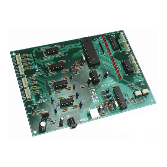
Construction 22. Rubber feet 21. IC's. Watch the position of the notch! Mount the rubber feet on the solder side of the PCB, see fig 1.0. IC1 : 6N136 IC2 : 6N136 IC3 : VK8061USB (programmed PIC18F2550-I/SP) IC4 : ULN2803 IC5 : ULN2803 IC6 : VK8061CPU (programmed PIC16F871-I/P) -
Page 9: Usb Connector
connection points USB-connector Connection of the K8061 with the USB port of your PC Power supply connection. Connect a 12V non-regulated adapter supply- 12VDC ing min. 300mA Digital inputs 1, 2, 3, 4 Inputs need to go “LOW” externally to activate (connect with the GND). Digital inputs 5, 6, 7, 8 These outputs are open collector outputs. -
Page 10: Software Installation
software installation 24. Software installation After assembly of the circuit, it is now time to install the software drivers and examples and to test the K8061. Connect a 12V power supply (non regulated 12V adapter) to the power supply connector of the K8061 (SK2). - Page 11 software installation Step 3 : Browse through the driver folder on your hard disk or included CD. Select driver : mchpusb.sys Step 4 : Click "Continue Anyway" Step 5 : Click "Finish"...
- Page 12 software installation Installation is successful A utility to check the operation of the K8061 can be found in the “DIAG8061” subfolder. A more elaborate test application can be found in the “DEMO8061” subfolder. The source code of the test application can be found in the “DLL examples” subfolder. Explanation concerning the communication DLL of the K8061 can be found in the “DOC”...
- Page 13 Connection example 25. How to connect : 1. Analog output : 2. Analog input : ANALOG OUTPUT VOLTAGE MAX 10V DC ! DAx : + 0 till 5V 0 ... 5V or 0 ... 10V 0 till 10V ADx : + 3.
- Page 14 Schematic diagram 26. Schematic diagram...
- Page 15 27. PCB layout.
- Page 16 VELLEMAN COMPONENTS Legen Heirweg 33 9890 Gavere Belgium Europe Info ?: http://www.velleman.be Modifications and typographical errors reserved © Velleman Kit nv H8061IP - 2006 - ED1 (rev. 1.0) 5 4 1 0 3 2 9 3 5 5 6 2 3...
Need help?
Do you have a question about the K4019 and is the answer not in the manual?
Questions and answers