Table of Contents
Advertisement
Advertisement
Table of Contents

Related Manuals for PQI DiskOnModule


Summary of Contents for PQI DiskOnModule
- Page 1 DG Series Datasheet...
- Page 2 Revision History Revision No History Draft Date Remark First document announced. 01/26/05 Preliminary...
-
Page 3: Table Of Contents
TABLE OF CONTENTS 1. Description…………………………………………………….……. 1 2. Features………………………………………………………….…. 1 3. Introduction………………………………………………….……… 2 4. Revision History............……..2 5. Specification………………………………………………..……..3 6. Installation Guide………………………………………………….. 5 7. Block Diagram………….……………………………………….…. 7 8. Pin Signal Assignment………………….………………………… 9 9. Interface Signal Assignments….……………..…….……………. 10 10. Signal Description………………...………………………...….…. 11 11. -
Page 4: Description
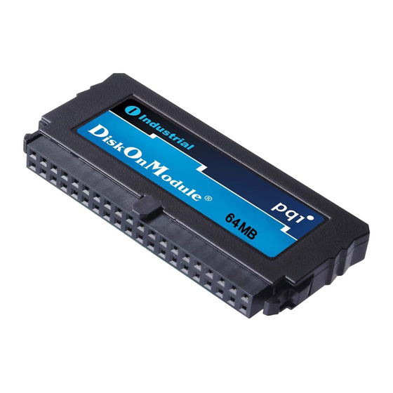
PQI’s DiskOnModule DG series based on NAND type flash memory controller technology. This product complies with 44 PIN IDE (ATA) standard interface and is suitable for data storage memory medium for portable system. By using DiskOnModule it is possible to operate good performance for the portable system which have IDE interface slots. -
Page 5: Introduction
PQI' s DiskOnModule is a storage device based on flash memory technology, which emulates an ordinary magnetic hard disk. The DiskOnModule series products provide an all in one module solution for solid-state flash disk. The DiskOnModule is suitable for use in portable and embedded systems which have limited space and power consumption. -
Page 6: Specification
Specification Environment Specifications 0 : to +70 : Operating Temperature (Industrial) -40 : to +85 : Non-Operating -40 : to +80 : Operating Temperature (WideTemp) -55 : to +95 : Non-Operating Relative Humidity 8% to 95% (with no condensation) Shock Operating 1000G Non-operating... - Page 7 Capacity Specifications Capacity Cylinder Head Sector Total sectors 16MB 1000 32000 32MB 64000 64MB 128000 128MB 256000 192MB 384000 256MB 1000 512000 512MB 1015 1023120 1024MB 2031 2047248 1536MB 3047 3071376...
-
Page 8: Installation Guide
Installation Guide BEFORE YOU BEGIN To protect your DOM from static discharge by making sure you are well grounded before touching the DOM. We recommend wearing a grounded wrist strap throughout the installation process. STEP 1 1. Make sure your computer is turned off before you open the case. 2. - Page 9 Option five allows you to select the drive you want to partition. Make sure that your new drive is selected. 4.Select "Create DOS partition or logical DOS drive" by pressing 1. Then press ENTER. 5.Select "Create primary DOS partition" by pressing 1 again. Then press ENTER. Create your first drive partition.
-
Page 10: Block Diagram
Block Diagram Flash Regulator Master/Slave Controller External Option DATA Hvcc BUFFER ATA(IDE) X`tal Interface DD0 to DD15 CS0, CS1 RESET DA0 to DA2 Flash memory bus DIOR DIOW INTRQ IORDY DATA FLASH ARRAY DASP , PDIAG Control signal... - Page 11 In order to gain the best management for flash memory, PQI DiskOnModule supports an efficient and swift algorithm. Due to the life of flash memory is limited, PQI try to increase the life of our flash product through the following arrangement. There are some blocks are reserved in flash memory and these blocks would not be used in normal operation.
-
Page 12: Pin Signal Assignment
Pin Signal Assignment The signals assigned for 44/40-pin applications are described in Table 1 Table 1 – Signal assignments for 44-pin ATA Signal name Connector Conductor Connector Signal name contact contact RESET- Ground DD10 DD11 DD12 DD13 DD14 DD15 Ground (keypin) or Vcc DMARQ Ground... -
Page 13: Interface Signal Assignments
Interface Signal Assignments And Descriptions Signal summary The physical interface consists of receivers and drivers communicating through a set of conductors using an asynchronous interface protocol. Table 2 defines the signal names. Table 2 - Interface signal name assignments Description Host Acronym Cable select... -
Page 14: Signal Description
Signal Descriptions CS0- (CHIP SELECT 0) This is the chip select signal from the host used to select the Command Block registers. CS1 – (CHIP SELECT 1) This is the chip select signal from the host used to select the Control Block registers. DA2, DA1, AND DA0 (DEVICE ADDRESS) This is the 3-bit binary coded address asserted by the host to access a register or data port in the device. - Page 15 INTRQ (Device interrupt) This signal is used to interrupt the host system. INTRQ is asserted only when the device has a pending interrupt, the device is selected, and the host has cleared the nIEN bit in the Device Control register. If the nIEN bit is equal to one, or the device is not selected, this output is in a h i g h im pe d a n c e s t at e , r e g a r d l e s s o f t he p r e s e n c e or a bs en c e of p e n d i n g interrupt.
-
Page 16: Interface Register Definition
Interface Register Definitions And Descriptions Device addressing considerations In traditional controller operation, only the selected device receives commands from the host following selection. In this standard, the register contents go to both devices (and their embedded controllers.) The host discriminates between the two by using the DEV bit in the Device/Head register. - Page 17 Table 3 - I/O port functions and selection address Addresses Functions CS0- CS1- Read (DIOR-) Write (DIOW-) × × × Data bus high Note used impedance Control block registers × × Data bus high Note used impedance × Data bus high Note used impedance Alternate Status...
- Page 18 [Duplicate Data, Error and Feature register] During word access, the address space occupied by the Data Register interferes with the space occupied by the Error register and Feature register, and reference cannot be made to these registers. Therefore, the PC Card ATA Standard provides an area where the copy of each register does not duplicate in the contiguous I/O mode and memory map mode.
-
Page 19: Physical Outline
Physical Outline DG0XXXX44NX0 (44 PIN) MASTER SALVE A Detail S=2:1...
Need help?
Do you have a question about the DiskOnModule and is the answer not in the manual?
Questions and answers