Table of Contents
Advertisement
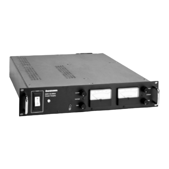
Sorensen
SORENSEN
Division of Elgar
9250 Brown Deer Road
San Diego, CA 92121-2294
1-800-525-2024
1-800-733-5427
Tel: (858) 450-0085
Fax: (858) 458-0267
Email: sales @ sorensen.com
sales@elgar.com
www.sorensen.com
www.elgar.com
This document contains information proprietary to Sorensen, Elgar Electronics Corporation. The information
contained herein is not to be duplicated or transferred in any manner without prior written permission from Sorensen.
March, 2000
DCR-B2 SERIES
500-Watt &1000-Watt
Power Supplies
Service Manual
Manual covers DCR-82 models:
500-Watt
10-4082
20-2582
40-1382
60-982
80-682
150-382
300-1.582
600-.7582
©2000 by Sorensen, Division of Elgar Electronics Corporation
1000-Watt
10-8082
20-5082
40-2582
60-1882
80-1282
150-682
300-382
600-1.582
Document No. M360645 Rev E
Advertisement
Table of Contents

Subscribe to Our Youtube Channel
Related Manuals for Sorensen DCR10-40B2


Summary of Contents for Sorensen DCR10-40B2
-
Page 1: Power Supplies
©2000 by Sorensen, Division of Elgar Electronics Corporation This document contains information proprietary to Sorensen, Elgar Electronics Corporation. The information contained herein is not to be duplicated or transferred in any manner without prior written permission from Sorensen. March, 2000... - Page 2 Buyer returns the defective product in the original, or equivalent, shipping container; • if, upon examination of such product by Sorensen it is disclosed that, in fact, a defect in materials and/or workmanship does exist, that the defect in the product was not caused by improper conditions, misuse, or negligence;...
-
Page 3: Table Of Contents
3.1 GENERAL............................17 3.1.1 CIRCUIT SYMBOL..........................17 3.1.2 SORENSEN PART NUMBER....................... 17 3.2 REPLACEMENT PARTS LISTS ...................... 17 3.3 ASSEMBLY DRAWINGS (SEE ATTACHED} ................. 17... - Page 4 LIST OF FIGURES TITLE FIGURE PAGE Phase Control Firing Angles .............. 1 DCR-B2 Functional Block Diagram ........... 2 1- 3 Passing Stage Principle ..............4 Performance Test Setup ..............12 LIST OF TABLES TABLE TITLE PAGE DCR-B2 Troubleshooting ..............11 Sensing Resistor Values ..............
-
Page 5: Theory Of Operation Page
--------------- SECTION 1 THEORY OF OPERATION ..........................INTRODUCTION This section provides a basic discussion of unit operating principles, which may be used in conjunction with the troubleshooting chart provided in Section 3, to enable the logical and rapid isolation of unit faults. A brief description of the phase control principle is given first, followed by a block diagram analysis of system functions. - Page 6 r------------------------------------------------------- 1 PCB ASSEMBLY COMPONENTS +16v REFERENCE -6.2v � SUPPL y -12.4v UA/02 (ETC.) -16v C.V. ERROR AMPLIFIER ' T · TURN-ON C.V. MODE RESET CIRCUIT INDICATOR CIRCUIT VARIABLE Q8/R6 REFER!.NCf --.---� ..a. J--- � � SHUTDOWN CIRCUIT COMPARATO!l C.C. MODE Q5/CR26,2/ ----·---- INDICATOR...
-
Page 7: Block Diagram Analysis (Figure 1-2)
..................BLOCK DIAGRAM ANALYSIS (FIGURE 1-2) The ac input voltage is first applied to CR? {l"riac), which is in series with power transformer T1 . CR? functions with the control circuits to form a feedback loop which prevents a change in output voltage when either the line or load changes. -
Page 8: Voltage Mode Section
ABSORBED INPUT VOLTAGE VOLTAGE PASSING STAGE l e__ ____ CONTROL Figure 1-3 Passing Stage Principle To illustrate circuit operation, assume an increase in the T2 (Figure 3-4) supply output. Pin 2 of U4 will become more negative, and the output at pin 6 more positive, tending to turn Q2 off. -
Page 9: Current Mode Section
Pin 3 of US is connected to plus sense. Front panel voltage controls R10/R11 function as variable feedback resistances from US pin 6 to pin 2. The negative 12.4 volt reference through R39/38/37 establishes the desired programming current range, so that Oto 10 volt signal is obtained at pin 6 of US. -
Page 10: Blocking Oscillator Circuit
The reset circuit consists of Q8 and R68. The full wave rectified ac input from T2 is impressed across O7/R48. 07 clamps the base of Q8 at its zener level, keeping it shut off (021 is forward biased). As the impressed voltage drops toward zero, the zener voltage follows. -
Page 11: Overvoltage Protector
1.4.7 ..........................POWER SECTION The input ac voltage is applied to the primary of power transformer T1 through an SCR, (CR7). The output is rectified by a full wave bridge, and filtered by a Pi network with a damping resistor (R3). -
Page 12: Changeable Current Programming Parameters
The input signal to U8 determines which lamp lights, as follows: Constant Current Mode (Current Limit) DS3 The input terminals of U8 are pins 2 and 3. Pin 2 is driven positive relative to pin 3 when the current amplifier (U7) output (pin 10) is in control (i.e., during current mode operation). -
Page 13: General
The troubleshooting data should be used in conjunction with the schematic diagrams and Section 1 which outlines the principles of operation. Any questions pertaining to repair should be directed to the nearest Sorensen representative or to the factory. - Page 14 Verify unit has gone from voltage mode to current mode by noting a significant drop in output voltage, by illumination of DS3. Set fine current adjustment to midpoint and apply short circuit. Using minimum current Adj. (R17 on PCB) adjust output current to exactly 0 amps.
-
Page 15: Performance Testing
Table 2-1 DCR-82 Troubleshooting No output (voltage mode) Wrong input voltage Open fuses and circuit breaker* Reference voltages (check levels) Defective U6 or U5 Collector to emitter short on QB, Q6, Q3, Q5 orQ4 Q9 open or shorted Fuse opens or circuit CR? shorted* Input capacitors shorted* breaker trips... -
Page 16: Oltage Mode Regulation And Ripple
Figure 2-1 Performance Test Setup 2.5.1 ..................... Voltage Mode Regulation and Ripple To check voltage mode regulation and ripple, proceed as follows: Connect a sensitive digital voltmeter and an RMS ac voltmeter across unit output terminals per Figure 2-1. Select a current shunt per Table 2-2 with a DVM for current output readings. -
Page 17: Current Mode Regulation
Decrease ac input voltage to low line specification. Output voltage change should not exceed limits specified in Table 2-3. Close load switch and adjust load for rated current. Using high ac line specification and full load, verify ripple meets specification. 2.5.2 .................... -
Page 18: Sensing Resistor Values
Table 2-2 Sensing Resistor Values (Current Mode Regulation Check) OCR MODEL SENSE RESISTOR (Ohms) 10-4082 0.01, 10-8082 .00625, 20-2582 0.01, 20-5082 .0200, 40-1382 0.01, 40-2582 .0400, 25W 60-982 0.1, 25W 60-1882 .0556, 20W 80-682 0.1, 25W .0833, 12W 80-1282 150-382 0.1, 25W 150-682 .167, 6W... -
Page 19: Unit Calibration Specification
Table 2-3 Unit Calibration Specifications Regulation Voltage Current Ripple Transient Maximum Cur. Mode Model Mode Mode (mA) Volt Mode Deviation IComplianc Upper Lim. (mV) (mV) (Volts) Set Pt. (A) (Vdc) 10-4082 10-8082 20-2582 62 . 5 28.75 20-5082 40-1382 32.5 14.95 40-2582 60-982... -
Page 20: Hi-Pot Test Procedure
If it is essential to use the high potential test method, please contact the factory for information on special precautions that should be taken. CAUTION Sorensen Company cannot be held liable for any malfunctions resulting from the application of a high potential test (greater than 100V). -
Page 21: General
This is an alpha-numeric identification of the component as called out on the unit drawings. 3.1.2 Sorensen Part Number ..................The Sorensen part number should be used when ordering parts directly from: Sorensen Sales & Technical Support 9250 Brown Deer Road... - Page 23 DO NOT USE HARDWARE SUPPLIED WITH CAPACITORS. NOTES: UNLESS OTHERWISE SPECIFIED. ZONE/ REV f OESCRIPTIClN REVISIONS � INSTALL NUTS FINGER TIGHT. A I REL IO £' OD E_ 9 89A34D ASSEMBLE PER ELGAR WORKMANSHIP STANDARD SECURE CAPACITORS WITH TIEWRAPS WITHOUT DISTORTING DOCUMENT NO.
- Page 24 A ORIGINATED IID,1SIONS .,...,. B REVISED ZONEJRfV OESCRIPTION DA TE l APPR0\£0 C REVISED D REVISED PER ECO 89A377 880512 106) SEE DETAIL "C" PIN 1 COMPONENT SIDE E REVISED PER ECO 92A 148 8901l07 F REVISED PER ECO 92A537 891116 G REVISED PER ECO 92A713 920420...
- Page 25 R<\ISIONS NOTES: UNLESS OTHERWISE SPEC I F IED. Z<M/REV DESQIIPTION "' DATE "'T APPRO\-fD A REL TO MANUFAC. 8/6/B0 I 4 /J0/g1 I B REL PER ECO 91A ASSEMBLE PER ELGAR WORKMANSHIP STANDARD 9/21/•1 I DOCUMENT NO. 0050003-01. C REV PER ECO 91A169 &...
- Page 26 : □ : � /""\7)2x JX ( 13 L._A (R 11) (R 10) VIEW A-A � � • l4X • • • DCR xn:-XXXS2 Power Supply ��\\\\\llilllll//////l//// ,!f' �\\\\\\\\iilllil//1/b;;f// � � � C VOLTS ' � AMPERES � "-!! NOTES: &...
- Page 27 REVISIONS DESCRIPTION DAlE ZONE APPROl,El SEE SHEET 1 ---= u � ------ � (MODEL 10-40) "" ' G'h_ / 2X ""' '---./ WIRES � , ,, ,- - - , RJ � 5 J REF 0------- ""' - - _/ / REF \ 2 53)&...
- Page 28 DESCRIPTICW ZON£!R£VI """OHS NOTES: UNLESS OTHERWISE SPECIFIED. P I REV PlcR ECN N95O_37O ASSEMBLE PER ELGAR WORKMANSHIP STANOARD N I REDRAW FQFl C_l,ARl1Y & APPLY A THIN lAYER OF THERMAL GREASE, ITEM 39 DOCUMENT NO. 0050003-01. BEFORE INSTALLATION OF THE RECTIFIER. ITEM 18. R I REV PER ECN N95OJO9 USE ON -7 (.l00-1.5).
- Page 29 A \ RE\'lSED PER EC089Al77 2. ALL RESISTORS IN OHMS AND 1/4W ±1% UNLESS OTHERWISE SPECIFIED. I 8811115 J. • THESE COMPONENTS ARE ADDED BY SORENSEN, DEPENDING·ON MODEL. B I R£\1SED- PER ECOOOAl52 I QQQ.101! 4. NUMBERS IN PARENTHESES ARE FOR THE LM317H, NUMBERS NOT IN C l �...
- Page 30 �- - -- ----- - - _) '-- --- - -- ---' T. OIJT f"l-:.!H ::----'" L=== ==== ==== � --& ._ ___ _, ES� ACr- ---, 129000 ------------ ..:.:.f..-...--_.,_ : DCR80-6B2 DCR10-40B2 h7�7 " "' ;. . ct:: « ��.., "- ""- "-"' I>...
- Page 31 Rf:VISIONS ZON£j REV} � : � = � : � � � DESCRIPTION f DAlE I APPff0\£0 A I REL ffR �O 9�93 AR I 5/17/oo B JREVISED I\R I e /+/Oo .-'--'-':C...,-.-� AR I 0/ 7 / 00 C I REV PER l;Q_ 9Q_A60A AR j B/ 2 +/00 D I REV PER �O 90A690_ _ D11 ND EO.
- Page 32 REVISIONS DESCRIPTION DATE APPRO� A REDRAW FOR CLARl1Y UNLESS OTHERWISE SPECIFIED. NOTES: MS </4/95 8 REV PER _ECN N95O;l_7O MS L10L9 ALL DIMENSIONS ARE IN INCHES (mm). SLIDE-RAIL OPTION AVAILABLE. CASE I CONVECT10N COOUD �===;=== 1 9.J S (SO " ! : =================== ===- 1--- -_ -_ -_ -_ -_ -_-_ -_ -_ -_-_ -_ -_-_ -_,_ •...
- Page 33 RE'.1SIONS ZONE REV! DEsaflPTION DAlt I APPR:0¥£0 I SEE SHEET 1 soow 1000W □ DCRB0-682 DCR150-J82 PCB CONTROL ASS'f OCR2Q-7fi82 0CR10-4082 I OCR20-25B2 I 0CR40-1382 I DCRB0-982 I OCRS0-682 I 0CR150-JB2 I DCRJ00-1.582 I .75B2 OCR10-4082 CR60-1882 OCR-t-0-1392 OCR60-9B2 DCRBOO DRAWING NUMBER 1063005 1064104-2...
- Page 34 REVISIOHS ZONE\REV DESCRIPTION OAlE I APPRO\.ED SEE SHEET 1000W 500W PCB CONTROL ASSf DCRt0-4082 0CR20-25B2 DCRn0-18B2 DCRB0-682 DCR150-382 DCR20-2582 0CR60-982 0CRe0-6B2 DCRl00-382 OCRJ00-1.582 DCR600-.7582 DCRl0-40B2 DCR-40-1382 DCR60-9B2 OCR-1-0-1382 1063 00 5 DRAWING NUMBER 586055-209 588055-170 586055-122 586055-66 586055-99 586055-110 586055-203 586055-126 586055-51 106JU40-226...
- Page 35 RE\o'ISIONS ZONE\REV DESCRIPTION DAlE I A;PPAO\W SEE SHEET soow 1000W DCR.,0-5082 PCB CONTROL ASS'f OCRl0-4082 OCR20-2582 DCR4'0-1J82 I OCR60-982 OCRB0-692 OCR150-JB2 DCRJ00-1.582 I 0CR600-,75B2 DCR40-25B2 DCRB0-1282 OCR150-682 DCRJ00-3B2 DCRS00-1.582 OCR60-f882 DRAWING NUMBER 1063005 2.J5-7395P64 2+-2015-1 1064980-1 235-7'40<4P33 2.35-7395P67 24-2037-7 Cl< 235-7395P61 235-7395P55 586385-5...
- Page 36 ""'"""· ZOHSIREV NOTES: UNLESS OTHERWISE SPECIFIED. B j REVISED PER ECN N970566A <;_j REYI_S_ !; D PE_ILEC:_N N�801i2 Ql_REVISED PER ECN N981060 REYISE[1_PER ECN �0014 F I REVISED PER ECN N000297 1000W 500W 0CR600-1.582 FINAL >SSY DCRl0-4082 0CR20-2SB2 DCRS0-18B2 OCRW-1.382 I OCRSO 982 DCRB0-682 nt':R150-JB2...
Need help?
Do you have a question about the DCR10-40B2 and is the answer not in the manual?
Questions and answers