Advertisement
Quick Links
U
DESCRIPTIO
Demonstration circuit DC257 is a constant-frequency
step-down converter using an LTC
chronous regulator. It provides low input voltage, high
conversion efficiency for cell phones and other portable
electronics operating from one or two Li-Ion cells or three
to six NiCd cells. Constant 350kHz operation and up to
600mA output capability in an SO-8 package provide a low
noise, space-efficient solution for wireless applications.
The circuit highlights the capability of the LTC1707. De-
signed to work at low voltages, the input voltage (V
range from 2.85V to 8.5V. At V
shuts down and draws just a few microamperes, making
W
U
PERFOR A CE SU
SYMBOL
PARAMETER
V
Input Voltage Range
IN
V
Output Voltage
OUT
I
Pulse Skipping Mode Supply Current
Q
Burst Mode Enabled Supply Current
Shutdown Current
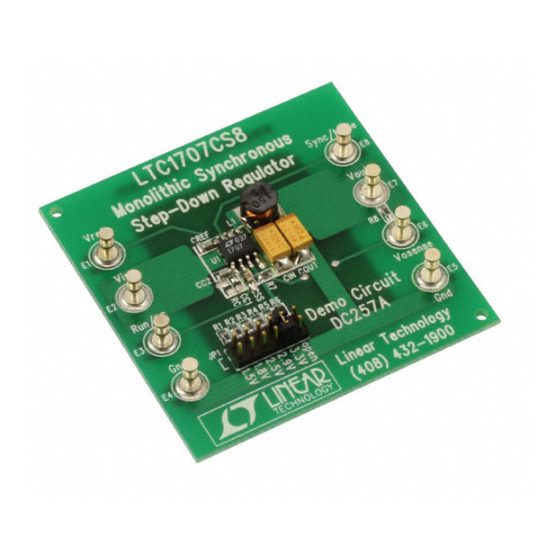
TYPICAL PERFOR A CE CHARACTERISTICS A D BOARD PHOTO
LTC1707 Efficiency Curve
100
V
= 3.3V
OUT
95
90
85
80
75
70
1
10
OUTPUT CURRENT (mA)
Synchronous Step-Down Regulator
®
1707 monolithic syn-
) can
IN
< 2.7V, the LTC1707
IN
W W
ARY
CONDITIONS
See Figure 2
V
= 5V, SYNC/MODE = 0V, RUN/SS = 2V, I
IN
V
= 5V, SYNC/MODE = 2V, RUN/SS = 2V, I
IN
V
= 5V, RUN/SS = 0V, I
IN
W
U
V
= 3.6V
IN
V
= 6V
IN
V
= 8.4V
IN
100
1000
DC257 TA01
DEMO MANUAL DC257
NO-DESIGN SWITCHER
LTC1707 Monolithic
it ideal for single lithium-ion battery applications. DC257's
output voltage is programmable from 1.5V to 3.3V via a
jumper.
At low output currents, the LTC1707 automatically switches
TM
to Burst Mode
operation to reduce switching losses and
maintain high operating efficiencies. In switching-noise
sensitive applications, Burst Mode operation can be inhib-
ited by grounding the SYNC/MODE pin or synchronizing it
with an external clock. Gerber files for this circuit board
are available. Call the LTC factory.
, LTC and LT are registered trademarks of Linear Technology Corporation.
Burst Mode is a trademark of Linear Technology Corporation.
= 0mA
OUT
= 0mA
OUT
= 0mA
OUT
U
Demo Board
JUMPER POSITION
2.85V to 8.5V
1.51V ±0.036V
JP1 = "1.5V"
1.82V ± 0.043V
JP1 = "1.8V"
2.52V ± 0.06V
JP1 = "2.5V"
2.94V ± 0.07V
JP1 = "2.9V"
3.33V ± 0.079V
JP1 = "3.3V"
JP1 = "OPEN"
JP1 = "3.3V"
JP1 = "3.3V"
JP1 = "3.3V"
VALUE
Note 1
300µA
200µA
15µA
1
Advertisement

Related Manuals for Linear Technology DC257


Summary of Contents for Linear Technology DC257
- Page 1 2.85V to 8.5V. At V < 2.7V, the LTC1707 , LTC and LT are registered trademarks of Linear Technology Corporation. shuts down and draws just a few microamperes, making Burst Mode is a trademark of Linear Technology Corporation.
- Page 2 DEMO MANUAL DC257 NO-DESIGN SWITCHER PERFOR A CE SU SYMBOL PARAMETER CONDITIONS JUMPER POSITION VALUE Minimum Output Current = 5V, V = 2.5V 600mA = 5V, V = 3.3V 500mA = 3V, V = 2.5V 300mA Operating Frequency Unsynchronized 350kHz...
-
Page 3: Parts List
DEMO MANUAL DC257 NO-DESIGN SWITCHER PARTS LIST REFERENCE DESIGNATOR QUANTITY PART NUMBER DESCRIPTION VENDOR TELEPHONE TPSC226M016R0375 22µF 16V TPS Tantalum Capacitor (207) 282-5111 TPSC107M006R0150 100µF 6V TPS Tantalum Capacitor (207) 282-5111 0603YC104KAT 0.1µF 16V X7R Chip Capacitor (843) 946-0362 06035A102JAT... -
Page 4: Quick Start Guide
DEMO MANUAL DC257 NO-DESIGN SWITCHER QUICK START GUIDE This demonstration board is easily set up to evaluate the Table 1. Output Voltage Selection performance of the LTC1707 IC. Please follow the proce- JP1 POSITION OUTPUT VOLTAGE dure outlined below for proper operation. - Page 5 DEMO MANUAL DC257 NO-DESIGN SWITCHER OPERATIO BURST Y = “0” ONLY WHEN X IS A CONSTANT “1” DEFEAT 1.5µA SLOPE SYNC/MODE COMP 0.4V – 0.6V FREQ SHIFT – SLEEP 6Ω – 0.8V 0.12V COMP – BURST 1.19V 2.25µA SWITCHING RUN/SOFT...
- Page 6 DEMO MANUAL DC257 NO-DESIGN SWITCHER OPERATIO When the converter uses Burst Mode operation, the peak maximum value. As C continues to charge, I is gradu- current of the inductor is set to approximately 200mA, ally released, allowing normal operation to resume.
- Page 7 DEMO MANUAL DC257 NO-DESIGN SWITCHER OPERATIO UNDERVOLTAGE LOCKOUT lower for V > 0.4 than when V < 0.4. See the maximum inductor peak current vs duty cycle graph in A precision undervoltage lockout shuts down the LTC1707 Figure 4. when V drops below 2.7V, making it ideal for single...
- Page 8 DEMO MANUAL DC257 NO-DESIGN SWITCHER OPERATIO MONOLITHIC SYNCHRONOUS SYNC/ STEP-DOWN REGULATOR MODE LTC1707CS8 10Ω RUN/SS LOAD OSENSE DEMO CIRCUIT DC257 Linear Technology (408) 432-1900 DC257 F05 Figure 5. Proper Measurement Setup CUT THIS TRACE MONOLITHIC SYNCHRONOUS SYNC/ STEP-DOWN REGULATOR MODE LTC1707CS8 10Ω...
- Page 9 DEMO MANUAL DC257 NO-DESIGN SWITCHER OPERATIO RUN/SOFT-START FUNCTION is a delay before starting of approximately 310ms/µF, followed by an additional 490ms/µF to reach full current. The RUN/SS pin (E3) is a dual-purpose pin that provides = 0.1µF on this PC board.
- Page 10 DEMO MANUAL DC257 NO-DESIGN SWITCHER PCB LAYOUT A D FIL Component Side Silkscreen Component Side Component Side Solder Mask...
- Page 11 Information furnished by Linear Technology Corporation is believed to be accurate and reliable. However, no responsibility is assumed for its use. Linear Technology Corporation makes no represen- tation that the interconnection of its circuits as described herein will not infringe on existing patent rights.
- Page 12 OF HOLES PLATED 0.020 PLTD 0.040 PLTD 0.072 NPLTD 0.095 PLTD TOTAL HOLES Linear Technology Corporation dc257f LT/TP 1099 500 • PRINTED IN USA 1630 McCarthy Blvd., Milpitas, CA 95035-7417 (408) 432-1900 FAX: (408) 434-0507 www.linear-tech.com © LINEAR TECHNOLOGY CORPORATION 1999...
- Page 13 Mouser Electronics Authorized Distributor Click to View Pricing, Inventory, Delivery & Lifecycle Information: Analog Devices Inc. DC257A...
Need help?
Do you have a question about the DC257 and is the answer not in the manual?
Questions and answers