
Related Manuals for abaco systems PPC11A


Summary of Contents for abaco systems PPC11A
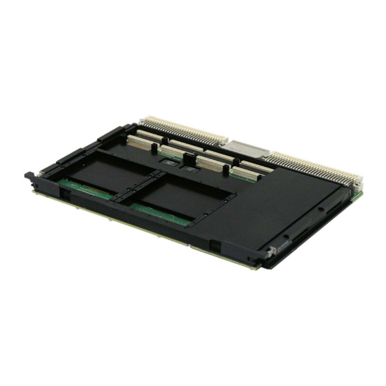
- Page 1 Hardware Reference Manual PPC11A 6U VME Single Board Computer Edition 1 Publication No. PPC11A-HRM/1...
-
Page 2: Document History
Directive 2012/19/EU of the European Parliament of 4 July 2012 on Waste Electrical and Electronic Equipment. Abaco Systems Limited will evaluate requests to take back products purchased by our customers before August 13, 2005 on a case by case basis. A WEEE management fee may apply. -
Page 3: About This Manual
About This Manual This manual contains hardware information for the Abaco Systems PPC11A SBC. The information contained in this manual must be read in conjunction with the PowerX Family Hardware Product Manual. LINK PowerX Range of SBCs Hardware Reference Manual, publication number PPC-0HH. - Page 4 You may need to register to access standards. Third Party Documents Due to the complexity of some of the parts used on the PPC11A, it is not possible to include the data on all such devices in this manual. A list of the specifications and...
- Page 5 CAUTION The PPC11A requires air-flow of at least 300 lfm for build levels 1 and 2, and at least 600 lfm for build level 3. If a conduction-cooled (level 4 or 5) PPC11A is operating on an extender card, it requires air-flow of at least 300 lfm across it.
-
Page 6: Table Of Contents
4.5.3 Paged Flash Mode ................................34 4.5.4 Flash Sector Protection ..............................34 4.6 SPI Serial Recovery Flash ........................... 35 4.7 NAND Flash Solid State Drive ..........................35 4.8 NVSRAM ................................35 continued overleaf 6 PPC11A 6U VME Single Board Computer Publication No. PPC11A-HRM/1... - Page 7 4.21 Timers ................................60 4.21.1 Watchdog Timer ................................60 4.21.2 AXIS Timer ..................................61 4.22 Baseboard Management Microcontroller ....................... 61 4.23 Resets and Interrupts ............................62 4.23.1 Hard Reset ..................................62 4.23.2 External Interrupt ................................63 Publication No. PPC11A-HRM/1 Contents 7...
- Page 8 5.16.10 GPIO (7-0) Interrupt Select Register (Offset 0x679) ....................82 5.16.11 GPIO (7-0) Interrupt Non-Maskable Register (Offset 0x67A) ................... 82 5.16.12 GPIO (7-0) Test Mode Register (Offset 0x67B) ......................83 8 PPC11A 6U VME Single Board Computer Publication No. PPC11A-HRM/1...
- Page 9 5.25 COM Port Loopback Enable Register (Offset 0x6BE) ..................94 5.26 SSD Erase Control Register (Offset 0x6BF) ....................95 5.27 SSD Cache Flush Control Register (Offset 0x6C0) ..................95 5.28 Scratch Pad Register 1 (Offset 0x6C6) ......................95 Publication No. PPC11A-HRM/1 Contents 9...
- Page 10 5.51.16 Watchdog Maximum Threshold High Byte Register (Offset 0x70F) ..............110 5.52 Scratchpad Memory Registers (Offset 0x720 to 0x72F) ................111 5.53 BMM UART Registers (Offsets 0x0 to 0x7) ....................111 10 PPC11A 6U VME Single Board Computer Publication No. PPC11A-HRM/1...
- Page 11 C.2.1 P2 Connector Alternative ............................142 C.3 PPC7D ................................143 C.3.1 P0 Connector ................................143 C.3.2 P0 Connector Alternative ............................144 C.3.3 P1 Connector ................................145 C.3.4 P2 Connector ................................146 C.3.1 P2 Connector Alternative ............................147 Publication No. PPC11A-HRM/1 Contents 11...
- Page 12 C.4.2 P1 Connector ................................150 C.4.3 P2 Connector ................................151 C.4.1 P2 Connector Alternative 1 ............................152 C.4.1 P2 Connector Alternative 2 ............................153 Glossary ............................. 154 Index ............................155 12 PPC11A 6U VME Single Board Computer Publication No. PPC11A-HRM/1...
- Page 13 Table 4-31 External Interrupt Inputs to Processor ...................... 62 Table 4-32 Processor PCI INTx and External IRQ Sharing ..................63 Table 4-33 LED Functions .............................. 67 Table 5-1 Control and Status Registers ........................70 Table 6-1 Connector Functions ........................... 112 Publication No. PPC11A-HRM/1 List of Tables 13...
- Page 14 Table A-4 Reliability (MTBF) ............................129 Table A-5 Mechanical Construction ........................... 129 Table A-6 Product Options ............................130 Table B-1 Volatile Memory ............................133 Table B-2 Non-Volatile Memory ..........................133 14 PPC11A 6U VME Single Board Computer Publication No. PPC11A-HRM/1...
- Page 15 Figure 1-3 Product Label (Conduction-cooled Product) ..................... 17 Figure 2-1 Link Positions ............................... 18 Figure 2-2 PMC/XMC Site Locations ..........................22 Figure 4-1 PPC11A General View ..........................26 Figure 4-2 Block Diagram (T2081) ..........................27 Figure 4-3 Block Diagram (T1042) ..........................28 Figure 4-4 Ethernet PHY Block Diagram ........................
-
Page 16: Unpacking
If you need to return the product, contact Abaco. The PPC11A is sealed into an antistatic bag and housed in a padded cardboard box. Failure to use the correct packaging when storing or shipping the PPC11A may invalidate the warranty. -
Page 17: Figure 1-3 Product Label (Conduction-Cooled Product)
Figure 1-3, attached to the front of the heatsink. Figure 1-3 Product Label (Conduction-cooled Product) PPC11A -48C111B4 CAGE CODE K7034 MADE IN UK See the Product Codes section in Appendix A for more details on the product code (PPC11A-xxxxxxxx). Publication No. PPC11A-HRM/1 Unpacking 17... -
Page 18: Configuration
2 • Configuration Link Configuration The PPC11A has push-on jumpers included in the standard kit of parts; additional jumpers may be obtained on request. These are suitable for level 1 to 3 low vibration applications. For Level 4 and 5 products, make links by wire-wrapping between the pin posts and then cover these wire-... -
Page 19: Inspection
Jumper Link Status Register (offset 0x6CD). If you are about to install your PPC11A and power-up for the first time, leaving it in the default configuration will enable board operation to be proven before tackling any further configuration issues. 2.3.1 Boot Area Selection Link (P15 Pins 1 to 4) The Boot Flash (for all processing cores) is divided into two sections, allowing for three different boot images to be loaded into the Flash. -
Page 20: Nvram Write Enable Link (P15 Pins 5 And 6)
2.3.2 NVRAM Write Enable Link (P15 Pins 5 and 6) This link controls the write protection for the NVRAM device on the PPC11A. This device holds firmware boot parameters as well as user data. Table 2-2 P15 Pins 5 and 6 Jumper Function... -
Page 21: Pmc1 & Pmc2 5V Vio Selection Links (P15 Pins 13 To 16)
2.3.6 Reserved Links (P17 and P18) These are reserved for use by Abaco only. Do not fit jumpers on these links Software Board Configuration The PPC11A contains two I EEPROM DIP Switch devices, which may be used to configure additional options under software control. For details on how to monitor or change these settings, see the appropriate software reference manual. -
Page 22: Mezzanine Installation
Mezzanine Installation As shown below, the PPC11A has two mezzanine sites that both support PMCs and ANSI/VITA42.3-compliant XMCs (including support for front-panel I/O in build levels 1 to 3). The two sites allow for the fitting of two single-width PMCs/XMCs or one double-width PMC/XMC. - Page 23 The power dissipation of any XMC fitted should be considered. An XMC with high power dissipation could cause the temperature of the PPC11A to rise beyond an acceptable limit. The magnitude of the effect of the XMC largely depends on the XMC thermal solution, and needs to be considered on a case-by-case basis.
-
Page 24: Installation And Power Up/Reset
PPC11A. The following notices also apply: CAUTION Consult the enclosure documentation to ensure that the PPC11A’s power requirements are compatible with those supplied by the backplane. Power Supply Requirements The PPC11A can only operate from a 5V main supply input. -
Page 25: Connecting To Ppc11A
The on-board power supplies are also monitored for correct operation, and the PPC11A is prevented from powering up and held in reset if any supply fails to operate correctly. -
Page 26: Functional Description
PCI-X operation at up to 133 MHz, allowing for off-the-shelf or custom PMCs to be fitted to add further functionality to the PPC11A. Both sites also support XMCs, providing a x4 PCIe link to each site, for higher bandwidth connectivity to the host and high-speed rear I/O (site 1 to P0 only). -
Page 27: Figure 4-2 Block Diagram (T2081)
Figure 4-2 Block Diagram (T2081) Publication No. PPC11A-HRM/1 Functional Description 27... -
Page 28: Figure 4-3 Block Diagram (T1042)
Figure 4-3 Block Diagram (T1042) NOTES Due to the increasingly short lifetimes of system components, the I/O devices used on the PPC11A are not guaranteed to remain fixed in the future. Hardware should be accessed only through mechanisms provided by the Operating System’s Board Support Package, and not directly by application software. -
Page 29: Features
Real-Time Clock • Elapsed time indicator • Ambient temperature sensors • System Management via BMM • I/O configurations that are pin-compatible with the PPC4A, PPC7A, PPC7D and • PPC10A Five environmental build levels • Publication No. PPC11A-HRM/1 Functional Description 29... -
Page 30: Integrated Host Processor
Freescale white paper “An Introduction to the QorIQ Platform’s Trust Architecture”. The PPC11A provides the ability to program fuses within the processor to configure security keys, access to which is controlled by the security state of the processor. -
Page 31: Memory Map
PPC11A from booting. When booting from the Recovery boot area, the Abaco-configured RCW settings are always used. This allows the PPC11A to be recovered if the data in the I C EEPROM is invalid or becomes corrupted. -
Page 32: Local Bus
4.3.7 Local Bus The T2081/T1042 local bus is a 16-bit multiplexed address/data bus that is used to access the following devices on the PPC11A: FPGA • Flash • • NVRAM All eight device chip selects for the local bus are made available, shared between the devices as defined in the table below. -
Page 33: Sdram
The memory interface can operate at 1600 MT/s. 4.4.1 Capacity The PPC11A provides 8 GB of SDRAM in a single bank, connected to a separate memory controller. The RAM configuration is defined below: Table 4-4 SDRAM Configuration... -
Page 34: Boot Flash
0x636). 4.5.4 Flash Sector Protection The PPC11A uses Cypress S29GL Flash devices, which provide advanced methods of sector protection to ensure the integrity of code data contained in the Flash array. Protection is defined on a per-sector basis, where a sector is 128 KB in size. Locked sectors cannot be erased or programmed, they may only be read. -
Page 35: Spi Serial Recovery Flash
Flash is protected by default and cannot be unprotected by the user. NAND Flash Solid State Drive The PPC11A optionally provides an on-board 32 GB NAND Flash Solid State Drive (SSD). The device used is a Silicon Motion SM651GEB SATA NANDrive device connected to a SATA port of a Marvell PCIe to SATA controller. -
Page 36: Vme Interface
VME Interface The PPC11A uses an IDT Universe II PCI-to-VME bridge, accessed from the processor PCIe interface via a Pericom PI7C9X110B PCIe to PCI bridge, to provide a full master/slave VME interface. The Universe IID is compliant with the following standards: American National Standard for VME64 (ANSI/VITA 1.0 - 1994 (R2002)) -
Page 37: Vmebus Master Access
VMEbus address to access any on-board address. The start address and size of window are programmable. VMEbus slave accesses to the PPC11A may be coupled, write posted or pre-fetched block read. Coupled slave transfers can only proceed once the slave posted write FIFO is empty. -
Page 38: Vmebus Master Block Transfers (Dma)
Several options are available, including stopping the operation and purging the offending transaction. A bus error during a DMA operation raises an interrupt and stops the DMA operation on the bus where the error was detected. 38 PPC11A 6U VME Single Board Computer Publication No. PPC11A-HRM/1... -
Page 39: Vmebus Retries
The PCI initiator requests a posted write cycle when the posted write FIFO can • accept no more entries The Universe II does not support the VMEbus RETRY~ signal. 4.10 The PPC11A has the following I/O connectivity: Ethernet • Serial Ports •... -
Page 40: Ethernet
ETH1_TXP ETH1_0P ETH0_TXN ETH0_0N ETH1_TXN ETH1_0N ETH0_RXP ETH0_1P ETH1_RXP ETH1_1P ETH0_RXN ETH0_1N ETH1_RXN ETH1_1N ETH0_2P ETH1_2P ETH0_2N ETH1_2N ETH0_3P ETH1_3P ETH0_3N ETH1_3N See the Product Codes section for more details. 40 PPC11A 6U VME Single Board Computer Publication No. PPC11A-HRM/1... -
Page 41: Serial Communication Ports
ETH2 and ETH3 are available with options PPC11A-xxx1xxxx and PPC11A-xxx7xxxx (see the Product Codes section for more details) as 10/100/1000BASE-T copper ports as follows: Table 4-9 ETH2/ETH3 10/100/1000BASE-T Pin Mapping Signal P2 Pin Signal P2 Pin ETH2_0P ETH3_0P ETH2_0N ETH3_0N... -
Page 42: Com3 To Com6
COM1 is always available. COM2 is available with options PPC11A-xxx1xxxx, PPC11A-xxx3xxxx and PPC11A-xxx5xxxx (see the Product Codes section for more details). The options to operate the ports in RS422 mode or to disable or loopback the transceivers, under software control, are provided by FPGA registers. The transceivers are disabled by default and must be enabled before any serial transfers can take place. -
Page 43: Host-To-Bmm Serial Port
Texas Instruments TPS2060 device, controlled by the processor. Both ports are present in all variants. Table 4-14 USB0/USB1 Signal Routing Signal P2 Pin Signal P2 Pin USB1_P USB2_P USB1_N USB2_N USB_PWR USB_PWR Publication No. PPC11A-HRM/1 Functional Description 43... -
Page 44: Sata
A Marvell 88SE9235 PCIe to SATA controller provides two Gen2 SATA backplane ports on the PPC11A. The device is connected to the processor via a PCIe switch. Both SATA ports (SATA0 and SATA1) are connected to the P0 connector. The two... -
Page 45: Table 4-16 Gpio Line Routing
If the alternate function is selected for any GPIO signal, its standard function is not available. The function selected is shown in EEPROM DIP Switch 1 Configuration Register 1 (offset 0x6EB). Publication No. PPC11A-HRM/1 Functional Description 45... -
Page 46: Mil-Std-1553
4.16 MIL-STD-1553 The PPC11A provides optionally provides up to two MIL-STD-1553 interfaces using DDC PCI Total-ACE devices. Each device provides a single dual-redundant 1553 transmission channel supporting both ‘transformer coupled’ and direct coupled’ outputs. 1553 is available with the following build variants: PPC11A-xxx2xxxx •... -
Page 47: Graphics
4.17 Graphics The PPC11A only supports graphics output when the T1042 processor is fitted. Options available are VGA on the P2 connector or DVI on the P0 connector. These options are mutually exclusive. 4.17.1 VGA VGA output is available with options PPC11A-xxx1xxxx and PPC11A-xxx3xxxx (see Product Codes section for more details). -
Page 48: Mezzanines
(PMC site empty) to conserve power. A pair of red LEDs, mounted on the back of the PPC11A, indicates the reset status of each bridge; when in reset, the LED is lit. A register in the FPGA can be used to control the reset line to each bridge, in software, as required. -
Page 49: Xmcs
The remaining XMC I/O signals are not available from this site. CAUTION The PMC user I/O and XMC user I/O are shorted together on the PPC11A, so take care when using PMCs/XMCs that can drive both types of I/O at the same time. -
Page 50: Table 4-20 Pmc/Xmc Site 1 Signal Availability
P14_IO_22 P14_IO_54 P16_IO_C19 P16_IO_D09 P14_IO_23 P14_IO_55 P16_IO_F18 P16_IO_E09 P14_IO_24 P14_IO_56 P16_IO_F19 P14_IO_25 P14_IO_57 P14_IO_26 P14_IO_58 P14_IO_27 P14_IO_59 P14_IO_28 P14_IO_60 P14_IO_29 P14_IO_61 P14_IO_30 P14_IO_62 = Differential pairs P14_IO_31 P14_IO_63 P14_IO_32 P14_IO_64 50 PPC11A 6U VME Single Board Computer Publication No. PPC11A-HRM/1... -
Page 51: Pmc/Xmc Site 2 Configuration
P24_IO_46 NOTES PMC site 2 user I/O (47:64) to P0 center rows is a build option over SATA. PMC site 2 I/O signals 53, 54, and 60 are not available on any build variant. Publication No. PPC11A-HRM/1 Functional Description 51... -
Page 52: Pcie Infrastructure
4.19.1 Processor The PPC11A supports a x4 link between the host processor and each central PCIe Switch (see overleaf). The link uses serdes lanes A to D on the host processor to connect to the first PCIe switch and serdes lanes E to H to connect to the second PCIe switch. -
Page 53: Pcie Switches
4.19.2 PCIe Switches The PPC11A has two PEX8619 16-lane PCIe switches, which connect the processor to PCIe devices as shown in Figures and 4-3. The default switch port configurations are shown below. Table 4-24 PCIe Switch 1 Connections Port Lane(s) - Page 54 10) link. The switch is prevented from accessing the EEPROM when in recovery mode so that the data may be recovered if it becomes corrupted. LEDs on the rear of the PPC11A show the status of the PCIe links. These are driven by I C expanders also connected to the private I C bus.
-
Page 55: I 2 C Buses
The PPC11A has three main I C buses: 1. The ‘Main’ Bus. This is internal to the PPC11A and provides access by the processor to various slave devices. 2. The ‘Sensor’ Bus. This is mastered by the Board Management Microcontroller (BMM) and provides access to various sensor devices. -
Page 56: Sensor And Backplane Buses
Table 4-27 I C Sensor Bus Addresses Device 7-Bit Address Power Manager 0x60 Temperature Sensors 0x18 XMC site 1 Set by the XMC XMC site 2 Set by the XMC 56 PPC11A 6U VME Single Board Computer Publication No. PPC11A-HRM/1... -
Page 57: I 2 C Bus 3
Configuration Write Enable Link (P15 pins 9 and 10) is fitted. 4.20.6 Elapsed Time Indicator A Maxim DS1682 Elapsed-Time Indicator logs the amount of time the PPC11A has been powered and the number of power cycles. Publication No. PPC11A-HRM/1 Functional Description 57... -
Page 58: Dip Switches
This is not currently implemented Not implemented NOTES The PPC11A must be reset for any updates to take effect. PMC1 and PMC2 5V VIO Selection Links (P15 Pins 13 to 16) override DIP Switch 1 register 0 bits 0 to 2 and DIP Switch 2 register 0 bits 0 to 2. -
Page 59: Real-Time Clock
The PPC11A has an STMicroelectronics LIS33HH motion sensor. 4.20.11 Power Manager The PPC11A uses a Lattice L-ASC10 power manager to sequence the power supplies in the required order for devices. The power manager also monitors each rail, and its voltage can be read from registers internal to the device, across the I C interface. -
Page 60: Timers
The Watchdog can be disabled by writing a “01” followed by “10” pattern to the relevant control register. The status of the Watchdog can also be read from this register. Watchdog Registers section for more details. 60 PPC11A 6U VME Single Board Computer Publication No. PPC11A-HRM/1... -
Page 61: Axis Timer
• VME geographic address • The BMM can reset or power-off the PPC11A in response to a request from software running on the processor or via commands over the backplane System Management bus. The BMM can control the state of the BIT Fail LED (DS402) to indicate BIT status. -
Page 62: Resets And Interrupts
The FPGA latches the cause of a hard reset and displays it in a Reset Cause Register (offset 0x61B or 0x61C) for software interrogation. When operating as the VME System Controller, the PPC11A asserts the VME SYSRESET~ signal when a hard reset occurs. 62 PPC11A 6U VME Single Board Computer... -
Page 63: External Interrupt
• Ethernet PHY • Temperature • GPIO • • Timer • • PCIe Switch The processor can determine the cause of the interrupt by reading an Interrupt Status register. Publication No. PPC11A-HRM/1 Functional Description 63... -
Page 64: Fpga
4.24 FPGA The PPC11A contains Lattice MachXO2 family Master and Slave FPGA devices. These implement various support functions such as: Glue logic • Reset control • Voltage translation • Watchdog • • Timers UART interface to the BMM • section 5 for the implemented register set. -
Page 65: Jtag
If a mezzanine site is populated, then the mezzanine must either implement JTAG or loop the chain through, otherwise the other site in the chain will not be reachable. The PPC11A provides no terminations for the mezzanine sites, since no active circuits are connected. -
Page 66: Leds
4.26 LEDs LEDs are mounted on the back of the PPC11A to reflect the status of the following functions: Power Supplies • • Reset status • • Ethernet links PCIe links • SATA activity • PCIe Switch status • Figure 4-10 LED Positions 66 PPC11A 6U VME Single Board Computer Publication No. -
Page 67: Ds10 And Ds43 To Ds45 (Bit)
FPGA or BMM. The green BIT Pass LED (DS43) is switched off at power up and is thereafter software-controlled. The user LEDs (DS44 and DS45) are switched off at power-up and are used by BIT, when they are illuminated yellow. See the PPC11A BIT documentation for more details. Once BIT has finished, these tri-color LEDs are software controlled and user-programmable. -
Page 68: Ds3 And Ds4 (Eth0 Status)
NOTE If you are fitting a non-Abaco PMC, it must comply with the standard for rugged, conduction-cooled PMCs (VITA20-2001) to ensure that it mates correctly with the PPC11A mechanics. Abaco PMCs comply with this standard. 68 PPC11A 6U VME Single Board Computer... -
Page 69: Air-Cooled Front Panel (Build Levels 1 To 3)
Figure 4-12 0.8” Air-cooled Front Panel XMC/PMC Sites The PPC11A front panel has provision for front I/O from both mezzanines. If a mezzanine has not been populated as part of an assembly with the PPC11A, then Abaco will fit a blanking plate at the site for EMC protection. -
Page 70: Control And Status Registers
5 • Control and Status Registers The PPC11A provides registers for software to control or read its status. The following table gives the locations of the registers, offset from the CS3 base address (which is configured by software), and access to the register:... - Page 71 Watchdog Warning Timer Bits 16:9 0x6C7 Test 0x70A Watchdog Minimum Threshold Low Byte 0x6C8 XMC/PMC Site 1 Status 0x70B Watchdog Minimum Threshold High Byte 0x6C9 XMC/PMC Site 2 Status 0x70C Watchdog Warning Threshold Low Byte Publication No. PPC11A-HRM/1 Control and Status Registers 71...
-
Page 72: Board Id Register (Offset 0X600)
0x2 = Rev 2 etc. Minor revision (hardware build state): 0x0 = Rev A 0x1 = Rev B etc. Master FPGA Revision Register (Offset 0x60B) Bits Description Major revision Minor revision 72 PPC11A 6U VME Single Board Computer Publication No. PPC11A-HRM/1... -
Page 73: Slave Fpga Revision Register (Offset 0X60B)
Minor revision Board ID String Register 1 (Offset 0x610) to Board ID String Register 11 (Offset 0x61A) These read back ASCII values for “PPC11A”. Offset 0x610 holds the first character and offset 0x61A holds the last character. NOTE Code should be written to read bytes until NULL is encountered or the last byte (0x61A) is reached. -
Page 74: Reset Cause Register 2 (Offset 0X61C)
Connected directly to BMM_PGM (program enable) pin BMM_PGD pin (= BIT Fail LED) output value - see also bit 4. This reads back the actual pin value regardless of the setting of bit 4 74 PPC11A 6U VME Single Board Computer Publication No. PPC11A-HRM/1... -
Page 75: Led Control Register 1 (Offset 0X622)
1 = Select recovery boot area (SPI) 0 = Select normal boot area Override boot source jumper links: 1 = Use bits 7 & 6 above 0 = Use jumper links/EEPROM DIP switch 4 to 0 Reserved 00000 Publication No. PPC11A-HRM/1 Control and Status Registers 75... -
Page 76: Pcie Sata Spi Control Register (Offset 0X626)
1 = BIT_HRESET request also causes a SYSRESET output 0 = BIT_HRESET request does not cause a SYSRESET output (default) This is independent of whether the PPC11A is System Controller. By itself, this bit does not generate a reset of any kind... -
Page 77: Nor Flash Page Register (Offset 0X636)
25 MHz (40 ns). NOTE Do not use this register when the PPC11A is an AXIS clock slave, as the frequency cannot be determined. Software may use this register to determine if the AXIS timer is implemented (it returns 0x00 if there is no AXIS timer). -
Page 78: Axis Clock Control Register (Offset 0X64F)
= 1:4 (500 kHz) = 1:8 (250 kHz) Enable Timer IRQ: 1 = IRQ enabled 0= IRQ masked This has a poor frequency tolerance, since it does not use a crystal source. 78 PPC11A 6U VME Single Board Computer Publication No. PPC11A-HRM/1... -
Page 79: Timer 0 Control/Status Register 2 (Offset 0X651), Timer 1 Control/Status Register 2 (Offset 0X659), Timer 2 Control/Status Register 2 (Offset 0X661) And Timer 3 Control/Status Register 2 (Offset 0X669)
Timer 1 Interrupt Clear Register (Offset 0x65A), Timer 2 Interrupt Clear Register (Offset 0x662) and Timer 3 Interrupt Clear Register (Offset 0x66A) Any write to this register clears the corresponding timer IRQ. Publication No. PPC11A-HRM/1 Control and Status Registers 79... -
Page 80: Timer Data Byte Registers
Reading a Timer Data Byte 0 register latches the upper bits of the Timer current counter value to prevent rollover (this may be the corresponding timer or all timers, depending on bit 4 of the Timer Control/Status Register 2). 80 PPC11A 6U VME Single Board Computer Publication No. PPC11A-HRM/1... -
Page 81: Gpio (7-0) Registers
For each GPIO, this register sets the interrupt detection sensitivity of each interrupt pin (active high/low or rising/falling edge depending on the level/edge mode): 1 = Active high/rising edge 0 = Active low/falling edge (default) Publication No. PPC11A-HRM/1 Control and Status Registers 81... -
Page 82: Gpio (7-0) Interrupt Both Edges Register (Offset 0X676)
0 = GPIO not available This register allows software to easily determine which of the GPIO7-0 signals are available on the PPC11A. All GPIO signals use shared backplane pins and are only available when the PPC11A is configured with the appropriate build option. -
Page 83: Gpio (7-0) Test Mode Register (Offset 0X67B)
0x686)) and enabled, then no further changes to any settings that affect that GPIO can be made (except for GPIO_TEST and GPIO_OUT). 5.17.5 GPIO (15-8) Interrupt Level/Edge Register (Offset 0x680) For each GPIO: 1 = Edge 0 = Level (default) Publication No. PPC11A-HRM/1 Control and Status Registers 83... -
Page 84: Gpio (15-8) Interrupt Polarity Register (Offset 0X681)
0 = GPIO not available This register allows software to easily determine which of the GPIO15-8 signals are available on the PPC11A. All GPIO signals use shared backplane pins and are only available when the PPC11A is configured with the appropriate build option. -
Page 85: Gpio (15-8) Interrupt Non-Maskable Register (Offset 0X686)
5.18 GPIO (23-16) Registers The PPC11A supports up to 19 GPIO lines, so in the following descriptions, bits 2 to 0 of each register map to GPIO pins 18 to 16 respectively. Bits 7 to 3 of each register are unused/reserved. -
Page 86: Gpio (23-16) Interrupt Enable Register (Offset 0X68B)
5.18.8 GPIO (23-16) Interrupt Status/Clear Register (Offset 0x68F) For each GPIO: 1 = Interrupt pending 0 = No interrupt (default) Write a ‘1’ to a bit to clear the interrupt pending status. 86 PPC11A 6U VME Single Board Computer Publication No. PPC11A-HRM/1... -
Page 87: Gpio (23-16) Availability Register (Offset 0X690)
0 = GPIO not available This register allows software to easily determine which of the GPIO23-16 signals are available on the PPC11A. All GPIO signals use shared backplane pins and are only available when the PPC11A is configured with the appropriate build option. -
Page 88: Availability Registers
5.20 Availability Registers These registers show whether a feature is available on the PPC11A. See the Functional Description for full details. NOTE Even when a feature is marked as unavailable in these registers, the device may still be visible to software, but may not be routed to backplane pins. -
Page 89: Com Port 4-Wire Configuration Register (Offset 0X6A2)
1 = COM port 2 is available in 4-wire (RS232/RS422) mode COM port 1 always supports 4-wire mode: 1 = COM port 1 is available in 4-wire (RS232/RS422) mode 5.20.4 COM Port Modem Configuration Register (Offset 0x6A3) The PPC11A does not support full modem lines. Bits Description Default... -
Page 90: Usb2.0 Ports 7-0 Availability Register (Offset 0X6A5)
1 = USB2.0 port is available USB2.0 port 0 is always available: 1 = USB2.0 port is available 5.20.7 USB3.0 Ports 7–0 Availability Register (Offset 0x6A6) There are no USB3.0 ports 7 to 0 available on PPC11A. Bits Description Default USB3.0 port 7:0 availability:... -
Page 91: Vga Availability Register (Offset 0X6Aa)
7 to 0 0x00 1 = Display-port is available 0 = Display-port is not available 5.20.14 Ancillary/Audio Availability Register (Offset 0x6AD) There is no front panel I/O or audio available on PPC11A. Bits Description Default Front panel I/O availability: 0 = Front panel I/O is not available... -
Page 92: Front Panel Configuration Register (Offset 0X6Ae)
5.20.15 Front Panel Configuration Register (Offset 0x6AE) There is no front panel I/O available on PPC11A. Bits Description Default 7 to 0 Feature availability: 0x00 0 = Feature not available 5.20.16 XMC/PMC Site 1 I/O Configuration Register (Offset 0x6AF) PMC1 I/O is fully P64 compliant. -
Page 93: Ssd Availability Register (Offset 0X6B1)
The transceivers for both COM1 and COM2 are enabled by the COM1 control; the COM2 control is ignored COM1 (and COM2) enable: 1 = COM port transceivers enabled 0 = COM port transceivers disabled Publication No. PPC11A-HRM/1 Control and Status Registers 93... -
Page 94: Com Port Mode Register (Offset 0X6Bc)
1 = COM port transceiver in RS422 mode 0 = COM port transceiver in RS232 mode 5.24 COM Port RS485 Auto-Direction Control Enable Register (Offset 0x6BD) The PPC11A does not support RS485 auto-direction control. Bits Description Default 7 & 6... -
Page 95: Ssd Erase Control Register (Offset 0X6Bf)
This is a generic read/write register available to software to validate FPGA access. It is sticky when reset using BIT_HRESET or CPU_RESET_REQ_L. This register is driven out in the processor POR_CFG word during Power-On/Reset. The default is 0x00. Publication No. PPC11A-HRM/1 Control and Status Registers 95... -
Page 96: Test Register (Offset 0X6C7)
1 = Force error detector to flag an error at the end of the current cycle 0 = Do not force error Setting this bit will cause the FPGA to reload and the PPC11A will reset Processor I C bus 2 to sensor bus buffer enable:... -
Page 97: Xmc/Pmc Site 1 Status Register (Offset 0X6C8)
XMC1 presence: 1 = XMC1 is fitted 0 = XMC1 is not fitted XMC1 VPWR voltage. The XMC VPWR rail is always 5V on PPC11A. 0 = XMC1 VPWR rail is 5V XMC1 BIST status: 1 = XMC1 BIST is active... -
Page 98: Xmc/Pmc Site 2 Status Register (Offset 0X6C9)
XMC2 presence: 1 = XMC2 is fitted 0 = XMC2 is not fitted XMC2 VPWR voltage. The XMC VPWR rail is always 5V on PPC11A. 0 = XMC2 VPWR rail is 5V XMC2 BIST status: 1 = XMC2 BIST is active... -
Page 99: Ssd Status Register (Offset 0X6Cb)
1 = Hardware write protection is active 0 = Hardware write protection is not active EEPROM DIP switches write protection status: 1 = Hardware write protection is active 0 = Hardware write protection is not active Publication No. PPC11A-HRM/1 Control and Status Registers 99... -
Page 100: Jumper Link Status Register (Offset 0X6Cd)
1 = Test card is fitted 0 = Test card is not fitted Flash protection unlock link (P15 pins 7 and 1 = Jumper is fitted 0 = No jumper fitted 100 PPC11A 6U VME Single Board Computer Publication No. PPC11A-HRM/1... -
Page 101: Boot Location Status Register (Offset 0X6Ce)
= PPC11A booted from Recovery area (SPI) = PPC11A booted from Main area (NOR Flash) SPD location. The PPC11A always boots using the SPD EEPROM located on-board 0 = Board booted using SPD EEPROM(s) located on-board Ethernet configuration ROM location. -
Page 102: Alarm Status Register (Offset 0X6D1)
The mapping of bits in the “(High)” registers to interrupt sources is as follows: Bits Interrupt Source Display Motion sensor 1 Motion sensor 2 BMM UART Timer (any) Watchdog PCIe switch 2 PCIe switch 1 102 PPC11A 6U VME Single Board Computer Publication No. PPC11A-HRM/1... -
Page 103: Interrupt Status Register (Low) (Offset 0X6E0)
0 = The interrupt source configured as maskable (default). 5.39.8 Interrupt Non-Maskable Register (High) (Offset 0x6E7) For interrupt bits in this register: 1 = The interrupt source is configured as non-maskable. 0 = The interrupt source configured as maskable (default). Publication No. PPC11A-HRM/1 Control and Status Registers 103... -
Page 104: Availability/Configuration Register (Offset 0X6E8)
0 = De-assert reset to XMC site 2 XMC site 1 reset control: 1 = Assert reset to XMC site 1 0 = De-assert reset to XMC site 1 1 & 0 Reserved 104 PPC11A 6U VME Single Board Computer Publication No. PPC11A-HRM/1... -
Page 105: Eeprom Dip Switch 1 Configuration Register 0 (Offset 0X6Ea)
5.42 EEPROM DIP Switch 1 Configuration Register 0 (Offset 0x6EA) This register returns the state of the EEPROM DIP Switch 1 Register 0 when the PPC11A was last reset. Only six bits are implemented. Bits Description Default 7 & 6... -
Page 106: Configuration Unlock Password Register (Offset 0X6Ec)
DS44 green segment control: 1 = Green segment switched on 0 = Green segment switched off DS44 blue segment control: 1 = Blue segment switched on 0 = Blue segment switched off 106 PPC11A 6U VME Single Board Computer Publication No. PPC11A-HRM/1... -
Page 107: Flash Password Registers (Offsets 0X6F0 To 0X6F7)
0x6F0 and byte 7 is at offset 0x6F7. 5.49 EEPROM DIP Switch 2 Configuration Register 1 (Offset 0x6FA) This register returns the state of the EEPROM DIP Switch 2 Register 0 when the PPC11A was last reset. Only 6 bits are implemented. Bits Description Default... -
Page 108: Watchdog Prescaler (Low Byte) Register (Offset 0X701)
Together with bit 7:4 of the Watchdog Enable Register, this determines the 12-bit division ratio used to generate the counting rate of the Watchdog. On the PPC11A, the input clock is 25 MHz. Program the desired division ratio minus 1, e.g. -
Page 109: Watchdog Kick Register (Offset 0X704)
Watchdog Status Register indicates whether this timer is running. NOTE The warning timer is a down counter. It may be treated as a 16-bit timer counting at half the rate of the main counter. Publication No. PPC11A-HRM/1 Control and Status Registers 109... -
Page 110: Watchdog Minimum Threshold Low Byte Register (Offset 0X70A)
This register holds the high byte of the 16-bit maximum threshold value. It defaults to 0x00. Configure this register before enabling the Watchdog. It is locked while the Watchdog is running (bit 0 of the Watchdog Enable Register is set). 110 PPC11A 6U VME Single Board Computer Publication No. PPC11A-HRM/1... -
Page 111: Scratchpad Memory Registers (Offset 0X720 To 0X72F)
The UART is accessed by a dedicated chip select (CS4), so its base address is software configurable. It is functionally equivalent to an industry-standard 16550 UART. See the Lattice “Reference Design RD1042” documentation for register details. Publication No. PPC11A-HRM/1 Control and Status Registers 111... -
Page 112: Connectors
Connectors Function J11, J12, J13, J14 PMC Site 1 J15, J16 XMC Site 1 J21, J22, J23, J24 PMC Site 2 XMC Site 2 Reserved Figure 6-1 Front Connector Positions 112 PPC11A 6U VME Single Board Computer Publication No. PPC11A-HRM/1... -
Page 113: Figure 6-2 Rear Connector Position
Figure 6-2 Rear Connector Position Publication No. PPC11A-HRM/1 Connectors 113... -
Page 114: Backplane Connectors
PMC1_46 XMC1_C19/ XMC1_B15/ XMC1_A15/ XMC1_E15/ XMC1_D15/ PMC1_55 PMC1_54 PMC1_53 PMC1_52 PMC1_51 XMC1_B17/ XMC1_A17/ XMC1_E17/ XMC1_D17/ XMC1_F19/ PMC1_60 PMC1_59 PMC1_58 PMC1_57 PMC1_56 Reserved XMC1_B19/ XMC1_A19/ XMC1_E19/ XMC1_D19/ PMC1_64 PMC1_63 PMC1_62 PMC1_61 114 PPC11A 6U VME Single Board Computer Publication No. PPC11A-HRM/1... -
Page 115: P1 Connector
BG0OUT~ BG1IN~ BG1OUT~ BG2IN~ BG2OUT~ SYSCLK BG3IN~ SYSFAIL~ BG3OUT~ BERR~ DS1~ BR0~ SYSRESET~ DS0~ BR1~ LWORD~ WRITE~ BR2~ BR3~ DTACK~ IACK~ IACKIN~ SMBUS_CLK IACKOUT~ SMBUS_DATA IRQ7~ IRQ6~ IRQ5~ IRQ4~ IRQ3~ IRQ2~ IRQ1~ -12V +5VSTDBY +12V Publication No. PPC11A-HRM/1 Connectors 115... -
Page 116: P2 Connector
COM6_RXD/PMC2_34 USB2_N BP_GPIO(16)/ETH2_3N/CH1_1553_TAG_CLK COM6_CTS/PMC2_36 PMC2_38 COM2_TXD BP_GPIO(17) PMC2_37 COM2_RXD BP_GPIO(18) PMC2_39 PMC2_41 COM2_RTS COM1_TXD PMC2_40 VGA_HSYNC/CH1_1553_IDCSAP COM1_RXD PMC2_42 PMC2_44 COM2_CTS/CH1_1553_ITCSAP COM1_RTS PMC2_43 VGA_RED/CH1_1553_ISGNDA COM1_CTS PMC2_45 PMC2_46 VGA_GREEN/CH1_1553_ITCSAN ENET0_2P VGA_BLUE/CH1_1553_IDCSAN ENET0_2N 116 PPC11A 6U VME Single Board Computer Publication No. PPC11A-HRM/1... -
Page 117: Backplane Signal Definitions
ETHx_Nn/P Gigabit Ethernet Channel (x=0-3) differential pair n (n = 0 to 3) EXT_RESET~ External Hard Reset Input. Pulling this input low will cause a hard reset to the PPC11A. Any switch logic should be debounced externally FLASH_PW_UL~ Replicates the effect of the... -
Page 118: Figure 6-3 Rs422/485 Signal Waveforms
VME -12V auxiliary power input. Connected to the PMC/XMC sites, otherwise unused by the PPC11A VME +5V power input +5VSTDBY Battery supply. Can be used to power the RTC on the PPC11A (requires up to 1µA) Figure 6-3 RS422/485 Signal Waveforms 118 PPC11A 6U VME Single Board Computer... -
Page 119: Pmc Connectors
P3V3 SERR~ C/BE1~ AD15 AD14 AD13 AD12 AD11 M66EN AD10 AD09 AD08 P3V3 C/BE0~ AD07 REQ_B~ AD06 AD05 P3V3 GNT_B~ AD04 PMC-RSVD (N/C) AD03 PMC-RSVD (N/C) EREADY AD02 AD01 RESET_OUT~ AD00 ACK64~ P3V3 REQ64~ MONARCH~ Publication No. PPC11A-HRM/1 Connectors 119... -
Page 120: J13/J23 Connector
AD53 AD52 AD51 AD50 AD49 AD48 AD47 AD46 AD45 AD44 AD43 AD42 AD41 AD40 AD39 AD38 AD37 AD36 AD35 AD34 AD33 AD32 PCI-RSVD (N/C) PCI-RSVD (N/C) PCI-RSVD (N/C) PCI-RSVD (N/C) 120 PPC11A 6U VME Single Board Computer Publication No. PPC11A-HRM/1... -
Page 121: J14/J24 Connector
PMC1_48 PMC2_47 PMC2_48 PMC1_49 PMC1_50 PMC2_49 PMC2_50 PMC1_51 PMC1_52 PMC2_51 PMC2_52 PMC1_53 PMC1_54 PMC2_53 PMC2_54 PMC1_55 PMC1_56 PMC2_55 PMC2_56 PMC1_57 PMC1_58 PMC2_57 PMC2_58 PMC1_59 PMC1_60 PMC2_59 PMC2_60 PMC1_61 PMC1_62 PMC2_61 PMC2_62 PMC1_63 PMC1_64 PMC2_63 PMC2_64 Publication No. PPC11A-HRM/1 Connectors 121... -
Page 122: Pmc Signal Descriptions
AD[63:00] Address/Data bits. Multiplexed address and data bus BUSMODE[2:4] Bus mode. Driven by the host to indicate the bus mode. On the PPC11A this is always PCI. BUSMODE2 is pulled-up. BUSMODE3 and BUSMODE4 are pulled down to GND BUSMODE1 Bus Mode 1. Driven low by a PMC if it supports the current bus mode. Used to detect the presence of a PMC on the site Command/Byte Enables. -
Page 123: Xmc Connectors
RESET_OUT~ P3V3 VPWR JTAG_TMS P12V_AUX P3V3 VPWR JTAG_TDI N12V_AUX VPWR JTAG_TDO PCIE_TX0P PCIE_TX0N MBIST~ PCIE_TX1P PCIE_TX1N VPWR PRESENT~ PCIE_TX2P PCIE_TX2N P3V3_AUX PCIE_TX3P PCIE_TX3N VPWR I2C_DATA VPWR NVMRO I2C CLK REFCLK_P REFCLK_N N/C (WAKE~) N/C (ROOT~) Publication No. PPC11A-HRM/1 Connectors 123... -
Page 124: J16 Connector
XMC1_IO_A13 XMC1_IO_B13 XMC1_IO_C13 XMC1_IO_D13 XMC1_IO_E13 XMC1_IO_F13 XMC1_IO_C14 XMC1_IO_F14 XMC1_IO_A15 XMC1_IO_B15 XMC1_IO_C15 XMC1_IO_D15 XMC1_IO_E15 XMC1_IO_F15 XMC1_IO_C16 XMC1_IO_F16 XMC1_IO_A17 XMC1_IO_B17 XMC1_IO_C17 XMC1_IO_D17 XMC1_IO_E17 XMC1_IO_F17 XMC1_IO_C18 XMC1_IO_F18 XMC1_IO_A19 XMC1_IO_B19 XMC1_IO_C19 XMC1_IO_D19 XMC1_IO_E19 XMC1_IO_F19 124 PPC11A 6U VME Single Board Computer Publication No. PPC11A-HRM/1... -
Page 125: Xmc Signal Descriptions
PCIe Receive Differential Pairs (from switch to XMC) PCIE_TX[3:0]P/N PCIe Transmit Differential Pairs (from XMC to switch) PRESENT~ XMC Present. Pulled low by the XMC to allow the PPC11A to detect if an XMC is fitted REFCLK_P/N PCIe Reference Clock. 100 MHz Differential clock to XMC RESET_IN~ XMC Reset In. -
Page 126: Test And Programming Headers
6.4.2 P14 (Test Access Card Connector) This is used to connect to the TAC. Pinout information is not provided here, as access to the signals can only be achieved using the TAC. 126 PPC11A 6U VME Single Board Computer Publication No. PPC11A-HRM/1... -
Page 127: A • Specifications
Time of Day/Calendar 1 second resolution. Standby power may be connected from the VBAT pin to maintain data during power down Logs the total accumulated time the PPC11A has been powered, and the Quarter second resolution number of power cycles... -
Page 128: Electrical Specification
CAUTION The minimum power off time supported by the PPC11A is 1 second. Power outages of less than 1 second may result in erroneous behavior from the PPC11A. The VME ±12V_AUX supplies are not used on the PPC11A and are not monitored but are connected to the PMC/XMC sites. -
Page 129: Reliability (Mtbf)
Level 1 to 3 ≈ 675g including the heatsink and front panel but excluding any mezzanines Dimensions The air-cooled PPC11A is constructed on a multi-layer 6U Eurocard and conforms to the dimensions specified in IEEE1101.1. The conduction-cooled PPC11A is constructed on a multi-layer 6U Eurocard and conforms to the dimensions specified in IEEE 1101.2... -
Page 130: Product Codes
5 = Build level 5 COM1, USB1 and USB2 are available in all options. See the Environmental Specifications section for more details on the build levels. The default product code is PPC11A-14C111B3. 130 PPC11A 6U VME Single Board Computer Publication No. PPC11A-HRM/1... -
Page 131: Software Support
Further tests can be invoked interactively, giving BIT a valuable role as a field service tool. Both object and source code products are available. Publication No. PPC11A-HRM/1 Specifications 131... -
Page 132: Background Condition Screening
LINK I/O Modules Hardware Reference Manual, publication number RT5154-0HH. A.8 Test Access Card The PPC11A supports the addition of a TAC to the rear of the board. This card provides the following functions: Access to JTAG chain via JTAG header •... -
Page 133: B • Statement Of Volatility
B • Statement of Volatility B.1 Volatile Memory The PPC11A contains volatile memory, i.e. memory in which the contents are lost when power is removed. None of this volatile memory is capable of write protection. Table B-1 Volatile Memory User... - Page 134 Elapsed-time recorder Erase via software user memory 32 GB Operating system and Flash (SATA NAND) Erase via software (optional) user data storage (some operating systems can implement a read-only file system) 134 PPC11A 6U VME Single Board Computer Publication No. PPC11A-HRM/1...
-
Page 135: C • Ppcx Compatibility
C • PPCx Compatibility This section shows PPC11A signal compatibility with the following PPCx boards: PPC4A • PPC7A • PPC7D • • PPC10A For full pinout details, see the appropriate board hardware reference manual. Compatibility of power and grounds is not highlighted. -
Page 136: P1 Connector
IACKIN~ SMBUS_CLK IACKOUT~ SMBUS_DATA IRQ7~ IRQ6~ IRQ5~ IRQ4~ IRQ3~ IRQ2~ IRQ1~ -12V +5VSTDBY +12V = PPC11A signal matches PPC4A signal = PPC11A signal is compatible with PPC4A (NC on PPC4A) 136 PPC11A 6U VME Single Board Computer Publication No. PPC11A-HRM/1... -
Page 137: P2 Connector
VGA_BLUE ENET0_2N USB mouse and keyboard could be used on USB1/2 for equivalence with PPC4A. = PPC11A signal matches PPC4A signal = PPC11A compatible with PPC4A at 10/100BASE-T only = PPC11A compatible with PPC4A-specific signal Publication No. PPC11A-HRM/1 Specifications 137... -
Page 138: P2 Connector Alternative
USB mouse and keyboard could be used on USB1/2 for equivalence with PPC4A. = PPC11A signal matches PPC4A signal = PPC11A compatible with PPC4A at 10/100BASE-T only = PPC11A compatible with PPC4A-specific signal 138 PPC11A 6U VME Single Board Computer... -
Page 139: Ppc7A
PMC1_52 PMC1_51 PMC1_60 PMC1_59 PMC1_58 PMC1_57 PMC1_56 Reserved PMC1_64 PMC1_63 PMC1_62 PMC1_61 PPC11A signals that are not compatible with PPC7A are greyed out. = PPC11A signal matches PPC7A signal = PPC11A compatible with PPC7A-specific signal Publication No. PPC11A-HRM/1 Specifications 139... -
Page 140: P1 Connector
IACKIN~ SMBUS_CLK IACKOUT~ SMBUS_DATA IRQ7~ IRQ6~ IRQ5~ IRQ4~ IRQ3~ IRQ2~ IRQ1~ -12V +5VSTDBY +12V = PPC11A signal matches PPC7A signal = PPC11A signal is compatible with PPC7A (NC on PPC7A) 140 PPC11A 6U VME Single Board Computer Publication No. PPC11A-HRM/1... -
Page 141: P2 Connector
Unused VGA_GREEN ENET0_2P VGA_BLUE ENET0_2N = PPC11A signal matches PPC7A signal = PPC11A signal is compatible with PPC7A (NC on PPC7A) = PPC11A compatible with PPC7A-specific signal = PPC11A compatible with PPC7A at 10/100BASE-T only Publication No. PPC11A-HRM/1 Specifications 141... -
Page 142: P2 Connector Alternative
PMC2_40 CH1_1553_IDCSAP COM1_RXD PMC2_42 PMC2_44 CH1_1553_ITCSAP COM1_RTS PMC2_43 CH1_1553_ISGNDA COM1_CTS PMC2_45 PMC2_46 CH1_1553_ITCSAN ENET0_2P CH1_1553_IDCSAN ENET0_2N = PPC11A signal matches PPC7A signal = PPC11A compatible with PPC7A at 10/100BASE-T only 142 PPC11A 6U VME Single Board Computer Publication No. PPC11A-HRM/1... -
Page 143: Ppc7D
PMC1_52 PMC1_51 PMC1_60 PMC1_59 PMC1_58 PMC1_57 PMC1_56 Reserved PMC1_64 PMC1_63 PMC1_62 PMC1_61 PPC11A signals that are not compatible with PPC7D are greyed out. = PPC11A signal matches PPC7D signal = PPC11A compatible with PPC7D-specific signal Publication No. PPC11A-HRM/1 Specifications 143... -
Page 144: P0 Connector Alternative
PMC1_57 PMC1_56 Reserved PMC1_64 PMC1_63 PMC1_62 PMC1_61 PPC11A signals that are not compatible with PPC7D are greyed out. = PPC11A signal matches PPC7D signal = PPC11A compatible with PPC7D-specific signal 144 PPC11A 6U VME Single Board Computer Publication No. PPC11A-HRM/1... -
Page 145: P1 Connector
SMBUS_CLK IACKOUT~ SMBUS_DATA IRQ7~ IRQ6~ IRQ5~ IRQ4~ IRQ3~ IRQ2~ IRQ1~ -12V +5VSTDBY +12V = PPC11A signal matches PPC7D signal = PPC11A signal is compatible with PPC7D (NC on PPC7D) = PPC11A compatible with PPC7D-specific signal Publication No. PPC11A-HRM/1 Specifications 145... -
Page 146: P2 Connector
ENET0_2P VGA_BLUE ENET0_2N = PPC11A signal matches PPC7D signal = PPC11A signal is compatible with PPC7D (NC on PPC7D) = PPC11A compatible with PPC7D-specific signal = PPC11A compatible with PPC7D at 10/100BASE-T only 146 PPC11A 6U VME Single Board Computer... -
Page 147: P2 Connector Alternative
BP_GPIO(18) PMC2_39 PMC2_41 COM2_RTS COM1_TXD PMC2_40 CH1_1553_IDCSAP COM1_RXD PMC2_42 PMC2_44 CH1_1553_ITCSAP COM1_RTS PMC2_43 CH1_1553_ISGNDA COM1_CTS PMC2_45 PMC2_46 CH1_1553_ITCSAN ENET0_2P CH1_1553_IDCSAN ENET0_2N = PPC11A signal matches PPC7D signal = PPC11A compatible with PPC7D at 10/100BASE-T only Publication No. PPC11A-HRM/1 Specifications 147... -
Page 148: Ppc10A
PMC1_57 PMC1_56 Reserved PMC1_64 PMC1_63 PMC1_62 PMC1_61 PPC11A signals that are not compatible with PPC10A are greyed out. = PPC11A signal matches PPC10A signal = PPC11A compatible with PPC10A-specific signal 148 PPC11A 6U VME Single Board Computer Publication No. PPC11A-HRM/1... -
Page 149: P0 Connector Alternative
XMC1_A11 XMC1_E11 XMC1_D11 XMC1_B13 XMC1_A13 XMC1_E13 XMC1_D13 XMC1_F18 XMC1_C19 XMC1_B15 XMC1_A15 XMC1_E15 XMC1_D15 XMC1_B17 XMC1_A17 XMC1_E17 XMC1_D17 XMC1_F19 Reserved XMC1_B19 XMC1_A19 XMC1_E19 XMC1_D19 = PPC11A signal matches PPC10A signal = PPC11A compatible with PPC10A-specific signal Publication No. PPC11A-HRM/1 Specifications 149... -
Page 150: P1 Connector
BR2~ BR3~ DTACK~ IACK~ IACKIN~ SMBUS_CLK IACKOUT~ SMBUS_DATA IRQ7~ IRQ6~ IRQ5~ IRQ4~ IRQ3~ IRQ2~ IRQ1~ -12V +5VSTDBY +12V = PPC11A signal matches PPC10A signal = PPC11A compatible with PPC10A-specific signal 150 PPC11A 6U VME Single Board Computer Publication No. PPC11A-HRM/1... -
Page 151: P2 Connector
BP_GPIO(18) Unused Unused COM2_RTS COM1_TXD Unused GN Unused D VGA_HSYNC COM1_RXD Unused COM2_CTS COM1_RTS Unused VGA_RED COM1_CTS Unused Unused VGA_GREEN ENET0_2P VGA_BLUE ENET0_2N = PPC11A signal matches PPC10A signal = PPC11A compatible with PPC10A-specific signal Publication No. PPC11A-HRM/1 Specifications 151... -
Page 152: P2 Connector Alternative 1
BP_GPIO(17) PMC2_37 COM2_RXD BP_GPIO(18) PMC2_39 PMC2_41 COM2_RTS COM1_TXD PMC2_40 CH1_1553_IDCSAP COM1_RXD PMC2_42 PMC2_44 CH1_1553_ITCSAP COM1_RTS PMC2_43 CH1_1553_ISGNDA COM1_CTS PMC2_45 PMC2_46 CH1_1553_ITCSAN ENET0_2P CH1_1553_IDCSAN ENET0_2N = PPC11A signal matches PPC10A signal 152 PPC11A 6U VME Single Board Computer Publication No. PPC11A-HRM/1... -
Page 153: P2 Connector Alternative 2
USB2_N CH1_1553_TAG_CLK PMC2_36 PMC2_38 COM2_TXD BP_GPIO(17) PMC2_37 COM2_RXD BP_GPIO(18) PMC2_39 PMC2_41 COM2_RTS COM1_TXD PMC2_40 CH1_1553_IDCSAP COM1_RXD PMC2_42 PMC2_44 CH1_1553_ITCSAP COM1_RTS PMC2_43 CH1_1553_ISGNDA COM1_CTS PMC2_45 PMC2_46 CH1_1553_ITCSAN ENET0_2P CH1_1553_IDCSAN ENET0_2N = PPC11A signal matches PPC10A signal Publication No. PPC11A-HRM/1 Specifications 153... -
Page 154: Glossary
Reset Configuration Word. Real-Time Clock. Rear Transition Module. Serial ATA. SATA Serial Management Bus. System on (a) Chip. Serial Presence Detect. Serial Peripheral Interface/Interconnect. Solid State Drive. Test Access Card. 154 PPC11A 6U VME Single Board Computer Publication No. PPC11A-HRM/1... -
Page 155: Index
PMC VIO Selection ..........21 Flash ................33 Positions ............... 18 Boot ................34 Software ..............21 NAND ..............35 Connecting to PPC11A ..........25 NOR ................33 Connectors ..............112 Paging ............... 34 Backplane ............... 114 Recovery ..............35 J11/J21 .............. - Page 156 COM Port Availability ........... 88 Motion Sensor............... 59 COM Port Enable ............ 93 MTBF ................129 COM Port Loopback Enable ........94 COM Port Mode ............94 COM Port Modem Configuration ......89 156 PPC11A 6U VME Single Board Computer Publication No. PPC11A-HRM/1...
- Page 157 Watchdog Warning Threshold......110 GPIO (7-0) Interrupt Status/Clear ......82 Watchdog Warning Timer ........109 GPIO (7-0) Out ............81 Write Protection Status .......... 99 XMC/PMC Site 1 I/O Configuration ..... 92 GPIO (7-0) Test Mode ..........83 Publication No. PPC11A-HRM/1 Index 157...
- Page 158 Statement of Memory Volatility....... 133 Sites ................48 System Controller ..........36, 98 TAC ................132 Connector ............... 126 Technical Specification ..........127 Temperature Sensor ............. 59 Timers ................60 Trust Architecture ............30 158 PPC11A 6U VME Single Board Computer Publication No. PPC11A-HRM/1...
- Page 159 1-866-652-2226 (866-OK-ABACO) Confidential Information - This document www.abaco.com contains Confidential/Proprietary Europe, Middle East and Africa: Information of Abaco Systems, Inc. and/or +44 (0)1327 359444 its suppliers or vendors. Distribution or reproduction prohibited without permission. THIS DOCUMENT AND ITS CONTENTS ARE PROVIDED "AS IS", WITH NO...
Need help?
Do you have a question about the PPC11A and is the answer not in the manual?
Questions and answers