
Related Manuals for abaco systems SBC329 3U VPX


Summary of Contents for abaco systems SBC329 3U VPX
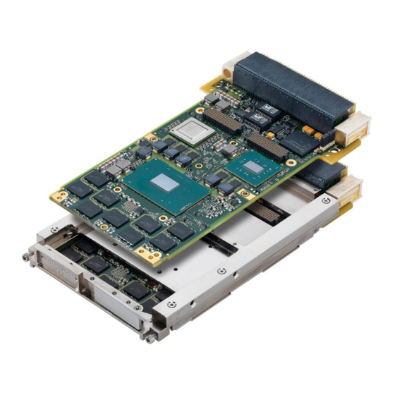
- Page 1 Hardware Reference Manual SBC329 3U VPX Single Board Computer Edition 1 Publication No. SBC329-HRM/1...
-
Page 2: Document History
Directive 2012/19/EU of the European Parliament of 4 July 2012 on Waste Electrical and Electronic Equipment. Abaco Systems Limited will evaluate requests to take back products purchased by our customers before August 13, 2005 on a case by case basis. A WEEE management fee may apply. -
Page 3: About This Manual
About This Manual Conventions Notices This manual may use the following types of notice: WARNING Warnings alert you to the risk of severe personal injury. CAUTION Cautions alert you to system danger or loss of data. NOTE Notes call attention to important features or instructions. Tips give guidance on procedures that may be tackled in several ways. -
Page 4: Further Information
IEEE 1101.10-1996 Additional Mechanical Specifications. ANSI/VITA 42.0-2008 XMC. ANSI/VITA 42.3-2006 XMC PCI Express Protocol Layer Standard. ANSI/VITA 46.0-2007 VPX Baseline Standard. VITA46.3-2012 Serial RapidIO on VPX. VITA46.4-2012 PCI Express on VPX. 4 SBC329 3U VPX Single Board Computer Publication No. SBC329-HRM/1... - Page 5 ANSI/VITA46.9-2010 XMC and PMC User I/O Mapping for VPX. VITA 46.11 (Draft) System Management on VPX. ANSI/VITA65-2010 OpenVPX System Specification. PCI Local Bus Specification Revision 2.1, PCI Special Interest Group. These are the latest versions at time of writing; check associated web sites for later updates.
-
Page 6: Technical Support
If you need to return a product, there is a Return Materials Authorization (RMA) tool available via the web site Embedded Support page. LINK https://www.abaco.com/embedded-support Do not return products without first contacting the Abaco Repairs facility. 6 SBC329 3U VPX Single Board Computer Publication No. SBC329-HRM/1... -
Page 7: Table Of Contents
Contents 1 • Introduction ......................15 1.1 Safety Notices ..........................16 1.1.1 Flammability ..............................16 1.1.2 EMI/EMC Regulatory Compliance ......................16 1.1.3 Cooling ................................17 1.1.4 Handling ............................... 17 1.1.5 Heatsink ............................... 17 2 • Unpacking ......................18 2.1 Box Contents Checklist ........................18 2.2 Identifying Your Board ........................ - Page 8 5.18 Baseboard Management Microcontroller ..................69 5.18.1 Board Temperature Sensor ........................70 5.18.2 PMBus Devices ............................71 5.19 Timers ............................72 5.19.1 General Purpose Timers ..........................72 5.19.2 Watchdog Timers ............................72 8 SBC329 3U VPX Single Board Computer Publication No. SBC329-HRM/1...
- Page 9 5 • Functional Description (continued) 5.20 LEDs .............................. 73 5.20.1 BIT LEDs (DS402 to DS404 and DS437) ....................74 5.20.2 Board Reset LED (DS405) ......................... 75 5.20.3 SSD Activity LED (DS408) ......................... 75 5.20.4 PCIe Link Status LEDs (DS409 to DS412) ....................75 5.20.5 POST Code LEDs (DS414 to DS421) ......................
- Page 10 6.46 SSD Status Register (0x6CB) ..................... 103 6.47 Write Protection Status Register (0x6CC) ................. 103 6.48 Board Jumper Link Status Register (0x6CD) ................104 6.49 Boot Location Status Register (0x6CE) ..................104 10 SBC329 3U VPX Single Board Computer Publication No. SBC329-HRM/1...
- Page 11 7 • Connectors ....................... 105 7.1 Backplane Connectors ......................... 107 7.1.1 P0 ................................107 7.1.2 Backplane J0 .............................. 107 7.1.3 P1 ................................108 7.1.4 Backplane J1 .............................. 108 7.1.5 P2 ................................109 7.1.6 Backplane J2 .............................. 110 7.1.7 Signal Descriptions ............................ 111 7.2 XMC Connectors ...........................
- Page 12 Table 7-2 P0 Pin Assignments ....................... 107 Table 7-3 J0 Pin Assignments ....................... 107 Table 7-4 P1 Pin Assignments ....................... 108 Table 7-5 J1 Pin Assignments ....................... 108 Table 7-6 P2 Pin Assignments ....................... 109 12 SBC329 3U VPX Single Board Computer Publication No. SBC329-HRM/1...
- Page 13 Table 7-7 J2 Pin Assignments ....................... 110 Table 7-8 Backplane Connector Signal Descriptions ................111 Table 7-9 J15 Pin Assignments ......................113 Table 7-10 J16 Pin Assignments ......................114 Table 7-11 XMC Signal Descriptions ...................... 115 Table A-1 Technical Data........................116 Table A-2 Voltage Supply Requirements ....................
- Page 14 Figure 5-11 Conduction-cooled Front Panel .................... 79 Figure 7-1 Front Connector Positions and Numbering ................105 Figure 7-2 Rear Connector Position and Numbering ................106 Figure 7-3 RS422/485 Signal Definition ....................112 14 SBC329 3U VPX Single Board Computer Publication No. SBC329-HRM/1...
-
Page 15: Introduction
1 • Introduction The Abaco Systems SBC329 is a member of the VPXcel3 family of 3U VPX Intel processor-based Single Board Computers. This family is aimed at processing, communications and display applications in the military and aerospace market. The PC-like SBC329 implements the Intel Kaby Lake Mobile (+ECC) architecture at up to 3.0 GHz, and has I/O interfaces including Gigabit Ethernet, USB 3.0, SATA and... -
Page 16: Safety Notices
1.1 Safety Notices The following general safety precautions represent warnings of certain dangers of which Abaco Systems is aware. Failure to comply with these or with specific Warnings and/or Cautions elsewhere in this manual violates safety standards of design, manufacture and intended use of the equipment. Abaco assumes no liability for the user’s failure to comply with these requirements. -
Page 17: Cooling
1.1.3 Cooling CAUTION The SBC329 requires air-flow of at least 300 for build levels 1 and 2, and at least 600 build level 3. If a conduction-cooled (level 4 or 5) SBC329 is operating on an extender card, it requires air-flow of at least 300 across it. -
Page 18: Unpacking
Figure 2-1 Product Label (Packaging) On the board within the antistatic bag, there is an identifying label, like the example shown in Figure 2-2, attached to the PCB. Figure 2-2 Product Label (Product) 18 SBC329 3U VPX Single Board Computer Publication No. SBC329-HRM/1... -
Page 19: Figure 2-3 Product Label (Conduction-Cooled Product)
On conduction-cooled versions of the board (build levels 4 and 5), there is also a label, like the example shown in Figure 2-3, attached to the front panel. Figure 2-3 Product Label (Conduction-cooled Product) See the Product Codes section in Appendix A for more details on the product code (SBC329-xxxxxxxxx). -
Page 20: Configuration
The diagram above shows standard 2.54 mm pitch headers for general use. This manual refers to jumper settings as In or Out. Meanings are as follows: In = jumper fitted - Out = jumper not fitted - 20 SBC329 3U VPX Single Board Computer Publication No. SBC329-HRM/1... -
Page 21: Inspection
3.2 Inspection The SBC329 is shipped from Abaco with no jumpers fitted. 3.3 Link Descriptions NOTES 1. Ordinary operation requires no jumpers to be fitted. 2. Software can read the state of the links from the FPGA. 3. Additional jumper link functions are provided by an on-board EEPROM DIP switch device. section 5.17.1. -
Page 22: Configuration Eeprom Write Enable Link (P6)
ETH1 and ETH2 Configuration EEPROM, Low (0) Frozen SPD EEPROM High (1) In or out Frozen EEPROM DIP Switch Low (0) Write enabled Low (0) Read only High (1) In or out Read only 22 SBC329 3U VPX Single Board Computer Publication No. SBC329-HRM/1... -
Page 23: Mezzanine Installation
3.4 Mezzanine Installation As shown in Figure 3-3, the SBC329 has one mezzanine site that supports a suitably compliant XMC (including support for front-panel I/O). CAUTION The SBC329 does not provide a fully compliant XMC site; the front I/O keepout area defined in the ANSI/VITA42 specification contains components. -
Page 24: Figure 3-3 Mezzanine Position
VITA 61 connectors, which offer a superior bandwidth and increased reliability. See the Product Codes section for more details. Figure 3-3 Mezzanine Position XMC Site 24 SBC329 3U VPX Single Board Computer Publication No. SBC329-HRM/1... -
Page 25: Installation And Power Up/Reset
4 • Installation and Power Up/Reset Review the Safety Notices in section 1 before installing the SBC329. The following notices also apply: CAUTION Consult the enclosure documentation to ensure that the SBC329’s power requirements are compatible with those supplied by the backplane. 4.1 Power Supply Requirements The SBC329 requires the backplane to provide 12V (VS1) , 3.3V (VS2), 5V (VS3) and... -
Page 26: Board Keying
Abaco I/O modules (or some equivalent system) ensures optimum operation of the SBC329 regarding EMI. See the VPX I/O Modules manual for more details. LINK VPX I/O Modules Hardware Reference Manual, publication number VPXIOM-0HH. 26 SBC329 3U VPX Single Board Computer Publication No. SBC329-HRM/1... -
Page 27: Connecting To Sbc329
4.4 Connecting to SBC329 To interact with on-board firmware requires the SBC329 to have connected, as a minimum, a video display (DVI or HDMI) and a USB keyboard. Ethernet and terminal (COM1) connections may also be required, depending on Operating System requirements. -
Page 28: Reset And Power-Up Sequence
If F7, Delete or Esc keys are not having the expected effect, either try using a USB keyboard or configuring your terminal program to send the function and escape sequences. 28 SBC329 3U VPX Single Board Computer Publication No. SBC329-HRM/1... -
Page 29: First Boot Menu
4.7 First Boot Menu This enables the user, for one time only, to select a drive device from which to boot. This feature is useful when installing from a bootable disk. For example, when installing an operating system from a CD, enter this menu and use the arrows keys to highlight ATAPI CD-ROM Drive. -
Page 30: About The Setup Menus
Save & Exit is activated, this is because one is not required, not because the user is then expected to reboot the board manually. 30 SBC329 3U VPX Single Board Computer Publication No. SBC329-HRM/1... -
Page 31: Main Menu
4.9 Main Menu This is the menu shown on entry to Setup. It reports details on the BIOS firmware, the board and the processor. It also allows the user to set the System Language (English is the default and currently the only option) and the SBC329 clock/calendar (although without battery back-up, any power cycle will reset the clock). -
Page 32: Advanced Menu
Setup. Select the Save & Exit menu, pick Restore Defaults then save these changes and reboot the board (e.g. by picking Save Changes and Reset). Figure 4-3 Advanced Menu 32 SBC329 3U VPX Single Board Computer Publication No. SBC329-HRM/1... -
Page 33: Chipset Menu
4.11 Chipset Menu This allows selection of the various options for the chipsets on the board (the System Agent configuration and PCH-IO configuration). The settings for the chipsets are processor-dependent; take care when changing settings from the defaults set by Abaco. CAUTION Changes made from some menus can cause the SBC329 to malfunction. -
Page 34: Abaco Menu
4.12 Abaco Menu This allows selection of the various options that are specific to the SBC329 (for example, the CPU speed locking configuration and DIP Switch settings). Figure 4-5 Abaco Menu 34 SBC329 3U VPX Single Board Computer Publication No. SBC329-HRM/1... -
Page 35: Board Build Information
4.12.1 Board Build Information When this item is selected, the SBC329 reports its specific build configuration (i.e. I/O options that depend on the variant ordered – see section A.6) to the user. Figure 4-6 Board Build Information Sub-menu Publication No. SBC329-HRM/1 Installation and Power Up/Reset 35... -
Page 36: Dip Switch Setup
PROGRAM DIP SWITCH NOTE Ensure that the DIP switch is write-enabled before selecting the option, PROGRAM DIP SWITCH by ensuring that the backplane NVMRO signal is inactive. Figure 4-7 DIP Switch Sub-menu 36 SBC329 3U VPX Single Board Computer Publication No. SBC329-HRM/1... -
Page 37: Fpga Setup/Status
4.12.3 FPGA Setup/Status This allows some on-board functions that are controlled by the FPGA to be configured and/or their status reported. To access these options, pick from the FPGA Abaco menu to display a sub-menu like the one shown below: Figure 4-8 FPGA Setup/Status Sub-menu Publication No. -
Page 38: Plx Switch Setup/Status
Settings are selected via this menu, and then activated by programming them into the configuration EEPROM. They are then loaded into the switch configuration registers the next time the board is reset or power cycled. Figure 4-9 PLX Switch Sub-menu 38 SBC329 3U VPX Single Board Computer Publication No. SBC329-HRM/1... - Page 39 XMC Speed This allows the speed (Gen1 @ 2.5 Gbits/second, Gen2 @ 5 Gbits/second or Gen3 @ 8 Gbits/second) of the XMC link to be set. NOTE Gen3 operation is not guaranteed, and its operation should be validated by the end user before use.
-
Page 40: Hardware Protection
4.12.5 Hardware Protection This allows the user to view or alter hardware protection. Figure 4-10 Hardware Protection Sub-menu 40 SBC329 3U VPX Single Board Computer Publication No. SBC329-HRM/1... -
Page 41: Cpu Speed Locking Configuration
4.12.6 CPU Speed Locking Configuration The maximum power (and hence the operating frequency) of the processor depends on the ability of the thermal solution to dissipate the heat generated by the processor. The processor will throttle its operating frequency to keep the junction temperature below the maximum level. -
Page 42: Enabling Booting Over A Network
Press F4 to save and exit the BIOS Setup menus. NOTE To boot from the network, some operating systems require that the network driver be set to ‘boot’ in the Control Panel. 42 SBC329 3U VPX Single Board Computer Publication No. SBC329-HRM/1... -
Page 43: Security Menu
4.13 Security Menu This menu allows setup of both an Administrator and a User password. The on- screen description covers use of these passwords. If both passwords are to be used, the Administrator password must be set first. Figure 4-13 Security Menu CAUTION Take care when setting passwords. -
Page 44: Boot Menu
Also available in this menu are Boot Configuration settings that allow the user to set how the SBC329 acts, for example, whether to use ‘Fast Boot’. Figure 4-14 Boot Menu 44 SBC329 3U VPX Single Board Computer Publication No. SBC329-HRM/1... -
Page 45: Save & Exit Menu
4.15 Save & Exit Menu This provides options on saving Setup selections and exiting Setup. Figure 4-15 Save & Exit Menu If changes have previously been made from the Setup menus, and the SBC329 malfunctions, reboot the board and select this screen. Pick then save Restore Defaults these changes and reboot the board (e.g. -
Page 46: Functional Description
Abaco-supported Operating Systems guarantee compatibility at the application level through hardware independent mechanisms. 46 SBC329 3U VPX Single Board Computer Publication No. SBC329-HRM/1... -
Page 47: Features
5.1 Features Based on Intel seventh-generation Xeon Mobile platform (Kaby Lake) Intel seventh-generation Xeon E3-1505M/L v6 processor, with four cores, at up to 3.0 GHz base frequency 16 GB of DDR4 SDRAM with ECC 32 GB SATA Solid State Drive storage ... -
Page 48: Microprocessor Subsystem
CPU operating frequency, a maximum temperature is achievable. This is further affected by the build level, which dictates the maximum ambient temperature at which the board can operate (see the Environmental Specification section). For more details, contact Abaco and see Appendix 48 SBC329 3U VPX Single Board Computer Publication No. SBC329-HRM/1... -
Page 49: Mobile Intel Cm238 Chipset (Pch)
5.2.2 Mobile Intel CM238 Chipset (PCH) The following features of the PCH are implemented on the SBC329: Two PCIe Gen2 x4 root ports SATA host controller supporting three ports at 6 Gbits/second (Gen3) LPC interface SPI interface for Boot Flash ... -
Page 50: Boot Flash
Software can read the write protection status, along with the SSD presence, from the FPGA. The FPGA also provides a Fast Erase facility. See relevant software documentation for information on how to activate this function. 50 SBC329 3U VPX Single Board Computer Publication No. SBC329-HRM/1... -
Page 51: Nvram
5.3.4 NVRAM A maximum of 1 MB of FRAM-type memory-mapped non-volatile memory is provided on the SBC329, and half of this is available to the user for general-purpose use. The remainder is allocated for system-only use, and is primarily used by BIT to store test results and sensor data. -
Page 52: Vpx Interface
Slot profiles define the physical layout of the fabric ports, whereas module profiles include information about the fabric protocol. A backplane will define a slot profile for each slot, but that slot is compatible with many module profiles. 52 SBC329 3U VPX Single Board Computer Publication No. SBC329-HRM/1... -
Page 53: Refclk
5.4.2 REFCLK The VPX REFCLK signal, on the P0 connector pins E8 and F8 can be optionally configured as a PCIe Gen3 compliant 100 MHz REFCLK signal. This can be connected to other boards in the backplane that are part of the PCIe bus segment. The SBC329 can also receive VPX REFCLK as a PCIe REFCLK signal, and use it to clock the backplane facing PCIe Non-Transparent ports for when the SBC329 is used as part of a peer-to-peer system. -
Page 54: I/O
PCIE_DP01_TX3N PCIE_DP02_TX3N Gen1 (2.5 GT/s per lane) and Gen2 (5 GT/s per lane) speeds are supported. Configuration of the link width and speed is provided by a BIOS setup menu. 54 SBC329 3U VPX Single Board Computer Publication No. SBC329-HRM/1... -
Page 55: Pcie Gen3 Operation
NOTES Backplane PCIe tracking operates only at Gen1 speed. The PCIe switch is Gen2 capable, but performance is limited to Gen1 to ensure robust operation. When connecting PCIe fabrics through cables such as those provided for use with the Abaco OpenVPX starter chassis (SCVPX3U-12), 5 GT/s operation may be possible but cannot be guaranteed. -
Page 56: Base-T + Base-Bx Variant (Sbc329-Xxx1Xxxxx)
When in this configuration, BASE-BX signals are connected to the ETH1 RJ-45 connector on the RTM. Do not use this connector for network connection! Permanent damage could be done to the SBC329 if these signals are connected to a live Ethernet network. 56 SBC329 3U VPX Single Board Computer Publication No. SBC329-HRM/1... -
Page 57: Dual Base-T Variant (Sbc329-Xxx2Xxxxx)
5.7.2 Dual BASE-T Variant (SBC329-xxx2xxxxx) In this configuration, ETH0 and ETH1 are configured as 10/100/1000BASE-T. ETH2 is not available in this configuration. The channels are connected to the VPX P1 connector as follows: Table 5-5 ETH0/ETH1 Pin Mapping - Dual BASE-T Variant Signal P1 Pin Signal... -
Page 58: Pcie Switch
EEPROM, as this could prevent the board from booting. NOTE If third party tools are being used to program the EEPROM, it must still first be write-enabled by the BIOS setup option. 58 SBC329 3U VPX Single Board Computer Publication No. SBC329-HRM/1... -
Page 59: Usb
5.10 USB The PCH provides up to three USB ports using XHCI controllers. These ports are called USB_P0, USB_P1 and USB_P2 from here on. USB_P0 and USB_P1 are always available; USB_P2 is available as a build option and its backplane connections are shared with XMC user I/O (see the Product Codes section). -
Page 60: Serial Ports
P2/G3 COM2_CTS COM2_RXD_B P2/G9 COM2_RTS COM2_TXD_B P2/G7 COM1 and COM2 are connected using a single Intersil ISL 41334 transceiver, which provides 15 kVolts ESD protection. Figure 5-5 RS422/485 Signal Definition 60 SBC329 3U VPX Single Board Computer Publication No. SBC329-HRM/1... -
Page 61: Rs422/Rs485 Mode
5.11.1 RS422/RS485 Mode The mode of operation for COM2 (i.e. RS232/RS422/RS485) can be configured in the BIOS, by selecting the relevant option in the EEPROM DIP switch, which is accessible through the BIOS setup screen. By default, this is set to RS232. COM2 supports RS485 Auto Direction Control, which automatically enables the RS485 transceiver when a character is ready to be transmitted. -
Page 62: Video
ESD protection is provided on all video signals. LINK For more information on the integrated Graphics Controller, see http://www.Intel.com. 62 SBC329 3U VPX Single Board Computer Publication No. SBC329-HRM/1... -
Page 63: Lpc Bus
5.14 LPC Bus The PCH is the master of an LPC bus, which is connected to the devices below. 5.14.1 FPGA A Microsemi Smart Fusion 2 provides various functions. See section 5.22 for more details. 5.14.2 Trusted Platform Monitor The SBC329 includes a Trusted Platform Monitor (TPM) device for security key generation and storage. -
Page 64: Mezzanine Site
85 Ω. All pairs (inter-pair) within each signal group (i.e. X8d and X12d) are length matched to within 0.5 inches. Each signal within a pair (intra-pair) is length matched to 10 thousandths of an inch. 64 SBC329 3U VPX Single Board Computer Publication No. SBC329-HRM/1... -
Page 65: Table 5-15 Mezzanine Site Signal Mapping
Table 5-15 Mezzanine Site Signal Mapping XMC I/O P2 Pin XMC I/O P2 Pin XMC I/O P2 Pin J16_IO_C08 J16_IO_A01 J16_IO_A05 J16_IO_C09 J16_IO_B01 J16_IO_B05 J16_IO_F08 J16_IO_D01 J16_IO_D05 J16_IO_F09 J16_IO_E01 J16_IO_E05 J16_IO_C10 J16_IO_A03 J16_IO_A07 J16_IO_C11 J16_IO_B03 J16_IO_B07 J16_IO_F10 J16_IO_D03 J16_IO_D07 J16_IO_F11 J16_IO_E03 J16_IO_E07 J16_IO_C12... -
Page 66: Real Time Clock
0x4C 0x98 SPD EEPROM 0x50 0xA0 SPD temperature sensor 0x18 0x30 SPD control registers 0x30 to 0x37 0x60 to 0x6E PEX 8725 PCIe switch 0x70 0xE0 LIS331HH accelerometer 0x19 0x32 66 SBC329 3U VPX Single Board Computer Publication No. SBC329-HRM/1... -
Page 67: Eeprom Dip Switch
5.17.1 EEPROM DIP Switch A PCA9560 device is used to configure the following aspects of board operation: Table 5-17 DIP Switch Options Internal Register Output Function and Bit (Datasheet Name) REG0 bit 0 MUX_A Boot SPI select: 0 = Boot from main SPI site 1 = Boot from FSP SPI site REG0 bit 1 MUX_B... -
Page 68: Sdram Spd Eeprom
For more details on the ETI device, see http://www.maxim-ic.com. 5.17.4 Accelerometer An ST Microelectronics LIS331HH three-axis MEMS accelerometer is fitted to the SBC329. This device provides the ability to detect excessive vibration levels and board orientation. 68 SBC329 3U VPX Single Board Computer Publication No. SBC329-HRM/1... -
Page 69: Baseboard Management Microcontroller
5.18 Baseboard Management Microcontroller The SBC329 uses a microcontroller embedded in the Smart Fusion FPGA to function as a BMM for implementation of the VPX System Management function in accordance with VITA 46.11. The BMM is connected to the following interfaces: ... -
Page 70: Board Temperature Sensor
Table 5-19 Temperature Sensor Monitor Locations Location TPM442A Channel Local PCB Local PEX8725 Core Remote 1 Remote PCB Remote 2 Figure 5-8 Local and Remote PCB Sensor Locations Remote Local 70 SBC329 3U VPX Single Board Computer Publication No. SBC329-HRM/1... -
Page 71: Pmbus Devices
5.18.2 PMBus Devices A total of four PMBus-compatible devices are included on the SBC329, which allows software to sense various parameters. This data can be used by system health monitoring software (either on the SBC329 or on an external IPMI controller) to determine the health and status of on-board power supplies, and board power consumption. -
Page 72: Timers
FPGA. Once enabled, the Watchdog must be serviced periodically. If the timeout expires before the Watchdog is serviced, then a hard reset is generated. Software can also disable the Watchdog through the FPGA. 72 SBC329 3U VPX Single Board Computer Publication No. SBC329-HRM/1... -
Page 73: Leds
5.20 LEDs Figure 5-9 Rear LED Positions DS409 DS410 DS429 DS435 DS438 DS436 DS430 DS433 DS431 DS434 DS405 DS404 DS403 DS402 DS437 DS411 DS432 DS422 DS412 DS408 Table 5-21 LED Summary LEDs Name Color Meaning when lit DS402 BIT Status 2 Yellow Depends on BIT test DS403... -
Page 74: Bit Leds (Ds402 To Ds404 And Ds437)
(straight after a reset) or has run but failed. The yellow LEDs show progress through BIT, and so may provide information for debugging purposes in the event of failure. The green LED shows that BIT has passed. 74 SBC329 3U VPX Single Board Computer Publication No. SBC329-HRM/1... -
Page 75: Board Reset Led (Ds405)
Table 5-23 BIT Status LED Meanings BIT Fail LED BIT Passed Status (DS404) LED (DS437) BIT not yet run (Reset state) or BIT failed BIT complete and passed The BITFAIL~ G1) backplane signal is driven active low using an open-drain driver when the red LED is lit. -
Page 76: Post Code Leds (Ds414 To Ds421)
This yellow LED illuminates when the SBC329 is in one of the S3, S4 or S5 sleep states. 5.20.10 BMM Status LED (DS438) This yellow LED is controlled exclusively by the BMM. See the relevant software manual for more information. 76 SBC329 3U VPX Single Board Computer Publication No. SBC329-HRM/1... -
Page 77: Resets And Interrupts
5.21 Resets and Interrupts 5.21.1 Interrupt Controllers The PCH provides an ISA-compatible Programmable Interrupt Controller (PIC) that incorporates the functionality of two 82C59 interrupt controllers. These are cascaded so that 14 external and two internal interrupts are possible. In addition, the PCH supports a serial interrupt scheme. -
Page 78: Fpga
SBC329-xxxx1xxxx or SBC329-xxxx3xxxx). Also, these signals must not be connected to any external loads that can interfere with their operation. section 6.10 for information on the AXIS timestamp registers. 78 SBC329 3U VPX Single Board Computer Publication No. SBC329-HRM/1... -
Page 79: Front Panel
5.23 Front Panel 5.23.1 Air-cooled Versions (Build Levels 1 to 3) In build levels 1 to 3, the SBC329 supports the VITA 48.1 1” pitch form factor. Figure 5-10 Air-cooled Front Panel XMC Slot The SBC329 front panel has provision for front I/O from the XMC site. If an XMC has not been ordered as part of an assembly with the SBC329, then Abaco will fit a blanking plate in the slot for EMC protection. -
Page 80: Fpga Registers
Read only 0x673 GPIO Interrupt Enable Read/Write 0x6B8 UART Enable Read/Write 0x674 GPIO Level/Edge Read/Write 0x6BB COM Port Enable Read/Write 0x675 GPIO Active Low/High Read/Write 0x6BC COM Port Mode Read/Write 80 SBC329 3U VPX Single Board Computer Publication No. SBC329-HRM/1... -
Page 81: Board Id Register (0X600)
LPC I/O Port Description Access LPC I/O Port Description Access 0x6BD COM Port RS485 Auto Direction Control Read/Write 0x6C8 XMC Status Read only 0x6BE COM Port Loopback Enable Read/Write 0x6CA Backplane Status Read only 0x6BF SSD Erase Control Read/Write 0x6CB SSD Status Read only 0x6C0... -
Page 82: Watchdog Timer Registers
111 = 2 ms 110 = 32 ms 101 = 131 ms 100 = 262 ms 011 = 524 ms 010 = 2.1 s 001 = 33 s 000 = 66 s 82 SBC329 3U VPX Single Board Computer Publication No. SBC329-HRM/1... -
Page 83: Board Id String Registers (0X610 To 0X61A)
6.5 Board ID String Registers (0x610 to 0x61A) These read back ASCII values for “SBC329”, as follows: Register Value ASCII Default 0x53 0x53 0x42 0x42 0x43 0x43 0x33 0x33 0x32 0x32 0x39 0x39 616 to 61A 0x00 0x00 NOTE Code should be written to read bytes until the first NULL is encountered or the last byte is reached (0x61A). -
Page 84: Bit Control And Status Register (0X629)
User/ZHURe select: 0=User NVRAM device is enabled in the NVRAM address window 1=ZHURe NVRAM device is enabled in the NVRAM address window 2 to 0 Read/Write 64 KB page select 84 SBC329 3U VPX Single Board Computer Publication No. SBC329-HRM/1... -
Page 85: Axis Registers
6.10 AXIS Registers 6.10.1 AXIS Timestamp Registers (0x648 to 0x64D) These can be used to read the 48-bit timestamp. Reading register 0 latches the current timestamp value into registers 1 to 5, so register 0 must always be read first. AXIS Timestamp Register Address Timestamp Value Bits... -
Page 86: Timer Registers
Setting this bit in either timer Control and Status Register 2 latches all timers on a read of the timer least significant byte. 6.11.3 Timer 0 IRQ Clear Register (0x652) and Timer 1 IRQ Clear Register (0x65A) Any write to this register clears the timer IRQ. 86 SBC329 3U VPX Single Board Computer Publication No. SBC329-HRM/1... -
Page 87: Timer 0 Data Bytes 0 To 3 Registers (0X654 To 0X657)
6.12 Timer 0 Data Bytes 0 to 3 Registers (0x654 to 0x657) Reads The value read is either the current timer value or the timer load value, depending on bit 3 of the Timer 0 Control and Status Register 1 (T0C&SR1[3]). Register Name Value if T0C&SR1[3] = 0... -
Page 88: Timer 1 Data Bytes 0 To 3 Registers (0X65C To 0X65F)
0x65D Timer 1 Data Byte 1 8 to 15 0x65E Timer 1 Data Byte 2 16 to 23 0x65F Timer 1 Data Byte 3 (most significant byte) 24 to 31 88 SBC329 3U VPX Single Board Computer Publication No. SBC329-HRM/1... -
Page 89: Gpio Registers
6.14 GPIO Registers The GPIO pin to register bit mapping for the following GPIO registers is as follows: Table 6-2 GPIO Register Bit Mapping Bits Read/Write Description 7 to 4 Read only Reserved 3 to 0 Read/Write GPIO3 to GPIO0 respectively 6.14.1 GPIO Out Register (0x670) The value of this register is driven onto the GPIO pins when the direction mode is set to output. -
Page 90: Gpio Both Edges Register (0X676)
GPIO0 availability (shared with COM2_TXD/TXD_A signal): 1 =GPIO0 available 0 =GPIO0 not available 6.14.10 GPIO15 to GPIO8 Availability Register (0x684) As GPIO15 to GPIO8 are not supported on SBC329, this register returns 0x00. 90 SBC329 3U VPX Single Board Computer Publication No. SBC329-HRM/1... -
Page 91: Fpga Registers (Continued)
6.15 VPX GDISC1 Registers The GDISC1 pin to register bit mapping for the following registers is as follows: Bits Read/Write Description Read/Write GDISC1 6 to 0 Read only Reserved 6.15.1 VPX GDISC1 Out Register (0x688) The value of this register is driven onto the GDISC1 pin when the direction mode is set to output. -
Page 92: Vpx Gdisc1 Both Edges Register (0X68E)
0 = Ethernet port 1 is not available 1 = Ethernet port 1 is available Ethernet port 0 availability: 0 = Ethernet port 0 is not available 1 = Ethernet port 0 is available 92 SBC329 3U VPX Single Board Computer Publication No. SBC329-HRM/1... -
Page 93: Com Port Availability Register (0X6A1)
6.17 COM Port Availability Register (0x6A1) Availability of COM2 is build option dependent. Bits Description Default 7 to 2 COM ports 8 to 3 availability: 000000 COM ports 8 to 3 are not available. 0 = COM port is not available COM2 availability: 0 = COM2 is not available 1 = COM2 is available... -
Page 94: Sata Port Availability Register (0X6A4)
0 = USB2.0 port is not available 1 and 0 USB2.0 ports 1 and 0 availability: USB2.0 ports 1 and 0 are always available. 1 = USB2.0 port is available 94 SBC329 3U VPX Single Board Computer Publication No. SBC329-HRM/1... -
Page 95: Usb3.0 Port 7 To 0 Availability Register (0X6A6)
6.22 USB3.0 Port 7 to 0 Availability Register (0x6A6) Availability of USB3.0 port 2 is build option dependent. Bits Description Default 7 to 3 USB3.0 ports 7 to 3 availability: 00000 USB3.0 ports 7 to 3 are not available. 0 = USB3.0 port is not available USB3.0 port 2 availability: 0 = USB3.0 port is not available 1 = USB3.0 port is available... -
Page 96: Vga Display Availability Register (0X6Aa)
Front panel I/O availability: 0 = Front panel I/O not available on the SBC329 6 to 1 Reserved 000000 Audio availability: 0 = Audio is not available on the SBC329 96 SBC329 3U VPX Single Board Computer Publication No. SBC329-HRM/1... -
Page 97: Front Panel Configuration Register (0X6Ae)
6.30 Front Panel Configuration Register (0x6AE) As no front-panel I/O is present on the SBC329, this returns 0x00. For information purposes only, the bit to port mapping is as follows: Port Ethernet 1 SATA 1 USB2.0 1 Video 1 Ethernet 0 SATA 0 USB2.0 0 Video 0... -
Page 98: Ssd Availability Register (0X6B1)
0 = COM2 UART is disabled and will not respond to reads or writes Read/Write COM1 UART enable: 1 = COM1 UART is enabled 0 = COM1 UART is disabled and will not respond to reads or writes 98 SBC329 3U VPX Single Board Computer Publication No. SBC329-HRM/1... -
Page 99: Com Port Enable Register (0X6Bb)
6.35 COM Port Enable Register (0x6BB) Software should enable transceivers after setting the desired COM port mode (i.e. RS232/RS422). Setting either of bits 0 or 1 to a ‘1’ will enable both COM1 and COM2 transceivers. To disable transceivers, both of bits 0 and 1 must be cleared to ‘0’. Bits Read/Write Description... -
Page 100: Com Port Rs485 Auto Direction Control Register (0X6Bd)
1 = COM2 transceiver loopback mode enabled 0 = COM2 transceiver loopback disabled (normal operation) Read/Write COM1 loopback enable: 1 = COM1 transceiver loopback mode enabled 0 = COM1 transceiver loopback disabled (normal operation) 100 SBC329 3U VPX Single Board Computer Publication No. SBC329-HRM/1... -
Page 101: Ssd Erase Control Register (0X6Bf)
6.39 SSD Erase Control Register (0x6BF) To trigger a hardware erase, bit 0 must be written with a ‘1’, ’0’, ’1’ pattern on consecutive write cycles to this register. This is to protect against ‘accidental’ erase functions. The value read from this register represents the state of the output, not the last value written. -
Page 102: Scratchpad Register (0X6C6)
0 = Backplane NVMRO signal is negated VPX GAP pin status: 1 = GAP pin is high 0 = GAP pin is low 4 to 0 VPX GA4 to GA0 status (inverted) 102 SBC329 3U VPX Single Board Computer Publication No. SBC329-HRM/1... -
Page 103: Ssd Status Register (0X6Cb)
6.46 SSD Status Register (0x6CB) SSD write protection is set by the Serial EEPROM DIP switch. Bits Description Default 7 to 1 SSD7 to SSD1 write protect status: 0000000 SSD7 to SSD1 are not supported SSD0 write protect status: 0 = SSD0 is write protected 1 = SSD0 is not write protected 6.47 Write Protection Status Register (0x6CC) Bits... -
Page 104: Board Jumper Link Status Register (0X6Cd)
SBC329. Determined by the state of the SPD link on the TAC. The SBC329 does not support the use of the Ethernet configuration EEPROM located on the TAC. 104 SBC329 3U VPX Single Board Computer Publication No. SBC329-HRM/1... -
Page 105: Connectors
7 • Connectors Table 7-1 Connector Functions Connector Function P0, P1, P2 VPX interface J15, J16 XMC site P5 (on rear of PWB) Test Access Card Figure 7-1 Front Connector Positions and Numbering Upper Key A19 F19 A19 F19 Lower Key NOTE The SBC329’s guide pin receptacles are unkeyed by default, but may be keyed to customer requirements. -
Page 106: Figure 7-2 Rear Connector Position And Numbering
Figure 7-2 Rear Connector Position and Numbering 106 SBC329 3U VPX Single Board Computer Publication No. SBC329-HRM/1... -
Page 107: Backplane Connectors
7.1 Backplane Connectors The following sections show the pin assignments of the SBC329 VPX backplane connectors (P0 to P2). These are shown in the 7-row format as used in the VPX specifications. Also provided are the corresponding pinouts for the J0 to J2 backplane connectors. These are shown in the 9-row format. -
Page 108: Backplane J1
DVI0__CLK_P DVI0__CLK_N DVI0_DDC_SCL DVI0_DDC_SDA ETH0_0P ETH0_0N ETH0_1P ETH0_1N DVI0_HPD ETH0_2P ETH0_2N ETH0_3P ETH0_3N ETH1_0P/ ETH1_0N/ ETH1_1P/ ETH1_1N/ MSKABLE_RESET~ ETH2_RXP ETH2_RXN ETH2_TXP ETH2_TXN ETH1_2P/ ETH1_2N/ ETH1_3P/ ETH1_3N/ ETH1_RXP ETH1_RXN ETH1_TXP ETH1_TXN 108 SBC329 3U VPX Single Board Computer Publication No. SBC329-HRM/1... -
Page 109: Table 7-6 P2 Pin Assignments
7.1.5 P2 Table 7-6 P2 Pin Assignments XMC_F09 XMC_F08 XMC_C09 XMC_C08 BITFAIL~ XMC_F11 XMC_F10 XMC_C11 XMC_C10 XMC_F13/ XMC_F12/ XMC_C13/ XMC_C12/ COM2_TXD/TXD_A/ USB_P2_P USB_P2_N USB_P2_PWR USB_P2_PWR GPIO(0) XMC_F15/ XMC_F14/ XMC_C15/ XMC_C14/ USB3_P2_RXP USB3_P2_RXN USB3_P2_TXP USB3_P2_TXN XMC_F17/ XMC_F16/ XMC_C17/ XMC_C16/ COM2_RXD/RXD_A/ SATA1_RXP SATA1_RXN SATA1_TXP SATA1_TXN... -
Page 110: Backplane J2
DVI1_DATA_2N DVI1__CLK_P DVI1__CLK_N XMC_E05 XMC_D05 XMC_B05 XMC_A05 USB_P0_1_PWR XMC_E07 XMC_D07 XMC_B07 XMC_A07 XMC_E09 XMC_D09 XMC_B09 XMC_A09 USB_P1_N XMC_E15 XMC_D15 XMC_B15 XMC_A15 XMC_E17 XMC_D17 XMC_B17 XMC_A17 USB_P1_P XMC_E19 XMC_D19 XMC_B19 XMC_A19 110 SBC329 3U VPX Single Board Computer Publication No. SBC329-HRM/1... -
Page 111: Signal Descriptions
7.1.7 Signal Descriptions Table 7-8 Backplane Connector Signal Descriptions Signal Description VS1, VS2, VS3 VPX Vs1 (+12 V), Vs2 (+3.3 V) and Vs3 (+5 V) power inputs. See the Electrical Specification section for more details P3V3_AUX VPX +3.3 V DC auxiliary power input. See the Electrical Specification section for more details The DC voltage reference for the system... -
Page 112: Figure 7-3 Rs422/485 Signal Definition
Serial COM port 2 Ready To Send flow control signal (RS232 mode) or Transmit Data B signal (RS422 mode) COM2_CTS~/RXD_B Serial COM port 2 Clear To Send flow control signal (RS232 mode) or Receive Data B signal (RS422 mode) Figure 7-3 RS422/485 Signal Definition 112 SBC329 3U VPX Single Board Computer Publication No. SBC329-HRM/1... -
Page 113: Xmc Connectors
7.2 XMC Connectors The SBC329 is fitted with standard VITA 42 XMC compatible connectors. However, there is an option to upgrade to VITA 61 connectors, which offer a superior bandwidth and increased reliability. See the Product Codes section for more details. 7.2.1 J15 J15 supplies the PCIe interface signals for the XMC site. -
Page 114: J16
XMC_A13 XMC_B13 XMC_C13 XMC_D13 XMC_E13 XMC_F13 XMC_C14 XMC_F14 XMC_A15 XMC_B15 XMC_C15 XMC_D15 XMC_E15 XMC_F15 XMC_C16 XMC_F16 XMC_A17 XMC_B17 XMC_C17 XMC_D17 XMC_E17 XMC_F17 XMC_C18 XMC_F18 XMC_A19 XMC_B19 XMC_C19 XMC_D19 XMC_E19 XMC_F19 114 SBC329 3U VPX Single Board Computer Publication No. SBC329-HRM/1... -
Page 115: Signal Descriptions
7.2.3 Signal Descriptions Table 7-11 XMC Signal Descriptions Signal Description PCIE_TX[7:0]P/N PCIe Transmit Differential Pairs (from XMC to SBC329) PCIE_RX[7:0]P/N PCIe Receive Differential Pairs (from SBC329 to XMC) REFCLK_P/N PCIe Reference Clock. 100 MHz differential clock to XMC Signal Ground P3V3 +3.3 V supply pins VPWR... -
Page 116: A • Specifications
Due to limitations in the VPX backplane bandwidth capability, the use of signal re-drivers at the system level may be required to guarantee USB3.0 super speed operation. The RTMs for the SBC329 (VPX3UX301 and VPX3UX601) include re-drivers on the USB3_P2 signals. 116 SBC329 3U VPX Single Board Computer Publication No. SBC329-HRM/1... -
Page 117: Electrical Specification
A.2 Electrical Specification A.2.1 Voltage Supply Requirements The SBC329 requires the VPX Vs1 (+12V), Vs2 (+3.3V), Vs3 (+5V) and 3V3_AUX supplies. These must remain within the limits specified below. If any of the supplies is outside of these specifications at power-up, the SBC329 will fail to start. If the supplies fall outside of these limits during a powered state, the SBC329 is held in reset and all on-board supplies are shut down. -
Page 118: Power Consumption
Current consumption on the non-primary rails does not vary so much with load or environmental conditions. Table A-6 Current Consumption – 3.3V Rail (Vs2) Temperature (°C) Operation Current @ 3.3 V +25°C Typical 0.9 A Maximum 1.0 A 118 SBC329 3U VPX Single Board Computer Publication No. SBC329-HRM/1... -
Page 119: Table A-7 Current Consumption - 5V Rail (Vs3)
Table A-7 Current Consumption – 5V Rail (Vs3) Temperature (°C) Operation Current @ 5.0 V +25°C Typical 0.4 A Maximum 0.6 A NOTES Vs3 is used primarily to supply the primary power (VPWR) rail to the XMC site. Ensure that any XMC used does not cause the specified maximum supply current to be exceeded. -
Page 120: Current Consumption (Sbc329-Xxxxxx2Xx Variant)
The backplane supply rails can be powered up in any order, although the 12V rail (if used) must be stable no later than 200ms after all other rails are stable. 120 SBC329 3U VPX Single Board Computer Publication No. SBC329-HRM/1... -
Page 121: Mechanical Specification
A.3 Mechanical Specification Table A-13 Mechanical Construction Form Factor 3U, single slot. Depending on the build variant, the following form factors are supported: VITA48.1 1” pitch type 2 (without 2LM covers) VITA48.2 0.85” pitch types 1 & 2 available (with and without 2LM covers) VITA48.2 1”... -
Page 122: Environmental Specifications
Storage: -50 to +100 STD-810E (Level 5) 10 cycles, and restricted cooling. Conformally- Fig 514.4 – 8 for high 240 hours coated as standard. Optional ESS performance aircraft. ~12g RMS 122 SBC329 3U VPX Single Board Computer Publication No. SBC329-HRM/1... - Page 123 NOTES As shown above, the build level dictates the maximum ambient temperature at which the board can operate. As the temperature affects the CPU operating frequency, this means that for a given build level, a maximum CPU operating frequency is achievable. For more details, contact Abaco and see Appendix The power dissipation of any XMC fitted should be considered.
-
Page 124: Product Codes
CPU operating frequency, this means that for a given build level, a maximum CPU operating frequency is achievable. For more details, contact Abaco and see Appendix 124 SBC329 3U VPX Single Board Computer Publication No. SBC329-HRM/1... -
Page 125: Software Support
A.7 Software Support Abaco’s software strategy allows fully integrated system-level solutions to be realized easily and with confidence. Off-the-shelf, layered software modules deliver the most from low-level hardware features while exploiting the best high level debug and run-time functionality of popular COTS operating systems and communications modules. -
Page 126: I/O Modules
VPX I/O Modules Hardware Reference Manual, publication number VPXIOM-0HH. VPX3UX301 Hardware Reference Manual, publication number VPX3UX301-HRM. VPX3UX601 Hardware Reference Manual, publication number VPX3UX601-HRM. MEZSBC3U1 Hardware Reference Manual, publication number MEZSBC3U1-HRM. 126 SBC329 3U VPX Single Board Computer Publication No. SBC329-HRM/1... -
Page 127: Test Access Card
A.9 Test Access Card The SBC329 supports the addition of a TAC (order code SBC328TST-11) to the rear of the board. This card provides the following functions: Access to CPU and PCH JTAG chain via XDP socket or JTAG header ... -
Page 128: B • Thermal Derating
SBC329, depending on the XMC’s power dissipation and thermal solution. The processor speed can be fixed in the BIOS. See section 4.12.6 for more details 128 SBC329 3U VPX Single Board Computer Publication No. SBC329-HRM/1... -
Page 129: Processor Option 3: Low Power
B.2 Processor Option 3: Low Power Product codes are of the form SBC329-y3xxxxxxx, where “y” is the build level and “3” selects the low-power processor (1505L, 25W). See the Product Codes section for details of the other options. Table B-2 Maximum Processor Speed versus Maximum Temperature for Processor Option 3 Build Maximum CPU Rating at Maximum Operating Temperature... -
Page 130: C • Statement Of Volatility
256 bytes Real Time clock data Power off, including VBAT supply SRAM 35 Kbit Internal FPGA configuration Power-off SRAM 1536 bytes IPMI BMM program execution Power-off P3V3_AUX rail and storage 130 SBC329 3U VPX Single Board Computer Publication No. SBC329-HRM/1... -
Page 131: Non-Volatile Memory
C.2 Non-Volatile Memory The SBC329 contains non-volatile memory, i.e. memory in which the contents are retained when power is removed. Table C-2 Non-Volatile Memory Memory Type Size User User Access Write Function Process to Clear Modifiable? to Data? Protectable? SATA NAND 32 GB Solid State Flash drive stores Any hard drive formatting... -
Page 132: Glossary
PCI Express. POST Power-On Self-Test. Rear Transition Module. Stock Keep Unit. Serial Presence Detect. Solid State Drive. Test Access Card (SBC328TST). Thermal Design Power. Trusted Platform Monitor. eXtended Debug Port. 132 SBC329 3U VPX Single Board Computer Publication No. SBC329-HRM/1... -
Page 133: Index
Index Accelerometer ............... 68 Cautions ......... 16, 17, 23, 25, 27, 30, Airflow ................17 ............ 32, 33, 43, 56, 58, 61, 81 AXIS Support ..............78 Chassis Ground ............26 Configuration Board................. 23 Link ................20 BCS ................125 Configuration EEPROM Write Enable .... - Page 134 Product Codes ............18, 124 Inspection ..............21 Product Identification ..........18 Interrupt Controllers ........... 77 Profile ................121 Introduction ..............15 Jumpers ........ See Configuration (Links) Keying ................26 134 SBC329 3U VPX Single Board Computer Publication No. SBC329-HRM/1...
- Page 135 R (continued) Real-Time Clock ............66 Registers (continued) Recovery Boot ............... 21 SSD Availability ............98 REFCLK ................. 53 SSD Erase Control ..........101 Registers ................ 80 SSD Secure Hardware Erase Capability ....98 Ancillary/Audio Availability ......... 96 SSD Status .............. 103 AXIS Clock Control..........
- Page 136 Signal Descriptions ..........115 Temperature Sensors ........... 70 Site ................64 Thermal Derating ............128 Current Provision ..........120 Timers ................72 Trusted Platform Monitor ........... 63 Unpacking ..............18 USB................. 59 136 SBC329 3U VPX Single Board Computer Publication No. SBC329-HRM/1...
- Page 137 1-866-652-2226 (866-OK-ABACO) Confidential Information - This document www.abaco.com contains Confidential/Proprietary Europe, Middle East and Africa: Information of Abaco Systems, Inc. and/or +44 (0)1327 359444 its suppliers or vendors. Distribution or reproduction prohibited without permission. THIS DOCUMENT AND ITS CONTENTS ARE PROVIDED "AS IS", WITH NO...
Need help?
Do you have a question about the SBC329 3U VPX and is the answer not in the manual?
Questions and answers