Sign In
Upload
Manuals
Brands
abaco systems Manuals
Motherboard
SBC329 3U VPX
abaco systems SBC329 3U VPX Manuals
Manuals and User Guides for abaco systems SBC329 3U VPX. We have
1
abaco systems SBC329 3U VPX manual available for free PDF download: Hardware Reference Manual
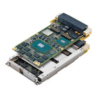
abaco systems SBC329 3U VPX Hardware Reference Manual (137 pages)
Brand:
abaco systems
| Category:
Motherboard
| Size: 5.01 MB
Table of Contents
Document History
2
About this Manual
3
Further Information
4
Technical Support
6
Table of Contents
7
1 Introduction
15
Figure 1-1 SBC329
15
Safety Notices
16
Flammability
16
EMI/EMC Regulatory Compliance
16
Cooling
17
Handling
17
Heatsink
17
Figure 1-2 ESD Label (Present on Board Packaging)
17
2 Unpacking
18
Box Contents Checklist
18
Identifying Your Board
18
Figure 2-1 Product Label (Packaging)
18
Figure 2-2 Product Label (Product)
18
Figure 2-3 Product Label (Conduction-Cooled Product)
19
3 Configuration
20
Link Configuration
20
Figure 3-1 Link Positions
20
Inspection
21
Link Descriptions
21
Recovery Boot Link (P3)
21
Table 3-1 P3 Link Setting
21
Configuration EEPROM Write Enable Link (P6)
22
Table 3-2 P6 Link Setting
22
Mezzanine Installation
23
Figure 3-2 Keepout Area
23
Figure 3-3 Mezzanine Position
24
4 Installation and Power Up/Reset
25
Power Supply Requirements
25
Table 4-1 Power Supply Requirements
25
Board Keying
26
Board Installation Notes
26
Connecting to SBC329
27
Reset and Power-Up Sequence
28
BIOS Setup Utility
28
First Boot Menu
29
Figure 4-1 First Boot Menu
29
About the Setup Menus
30
Main Menu
31
Figure 4-2 Main Menu
31
Advanced Menu
32
Figure 4-3 Advanced Menu
32
Chipset Menu
33
Figure 4-4 Chipset Menu
33
Abaco Menu
34
Figure 4-5 Abaco Menu
34
Board Build Information
35
Figure 4-6 Board Build Information Sub-Menu
35
DIP Switch Setup
36
Figure 4-7 DIP Switch Sub-Menu
36
Figure 4-8 FPGA Setup/Status Sub-Menu
37
FPGA Setup/Status
37
Figure 4-9 PLX Switch Sub-Menu
38
PLX Switch Setup/Status
38
Figure 4-10 Hardware Protection Sub-Menu
40
Hardware Protection
40
CPU Speed Locking Configuration
41
Figure 4-11 CPU Speed Locking Configuration Sub-Menu
41
Enabling Booting over a Network
42
Figure 4-12 Network Boot Configuration Sub-Menu
42
Security Menu
43
Figure 4-13 Security Menu
43
Boot Menu
44
Figure 4-14 Boot Menu
44
Save & Exit Menu
45
Figure 4-15 Save & Exit Menu
45
5 Functional Description
46
Figure 5-1 Block Diagram
46
Features
47
Microprocessor Subsystem
48
E3-1505M/L V6 Processor
48
Table 5-1 Supported Processor Skus
48
Mobile Intel CM238 Chipset (PCH)
49
Processor Debug Port
49
Memory
49
Sdram
49
Table 5-2 SDRAM Configuration
49
Boot Flash
50
Flash Hard Drive
50
Nvram
51
VPX Interface
52
Openvpx Compatibility
52
Figure 5-2 SLT3-PAY-2F2T-14.2.5 Port Layouts
52
Figure 5-3 SLT3-PAY-2F2U-14.2.3 Port Layouts
52
Refclk
53
Module Maskable Reset
53
Global Discrete
53
I/O
54
Data Plane Fabric
54
Table 5-3 Data Plane Pin Mapping
54
Pcie Gen3 Operation
55
Control Plane Fabric/Gigabit Ethernet
55
BASE-T + BASE-BX Variant (SBC329-Xxx1Xxxxx)
56
Table 5-4 ETH0/ETH1/ETH2 Pin Mapping - BASE-T + BASE-BX Variant
56
Figure 5-4 Gigabit Ethernet Channel Configurations
56
Dual BASE-T Variant (SBC329-Xxx2Xxxxx)
57
Gpio
57
Table 5-5 ETH0/ETH1 Pin Mapping - Dual BASE-T Variant
57
Table 5-6 GPIO Line Signal Availability
57
Pcie Switch
58
Switch Configuration EEPROM
58
Table 5-7 Pcie Switch Port Configuration
58
Usb
59
Table 5-8 USB Signal Availability
59
Serial Ports
60
Figure 5-5 RS422/485 Signal Definition
60
Table 5-10 COM1/COM2 Signal Availability
60
Table 5-9 COM Port Connections
60
RS422/RS485 Mode
61
Sata
61
Table 5-11 SATA Signal Availability
61
Video
62
Table 5-12 Video Port Summary
62
Table 5-13 DVI Signal Mapping
62
LPC Bus
63
Fpga
63
Trusted Platform Monitor
63
Mezzanine Site
64
XMC Connectors
64
I/O Routing
64
Table 5-14 XMC I/O Routing Availability
64
Table 5-15 Mezzanine Site Signal Mapping
65
Real Time Clock
66
I 2 C Bus
66
Figure 5-6 I 2 C Bus Structure
66
Table 5-16 I 2 C Bus Addresses
66
EEPROM DIP Switch
67
Table 5-17 DIP Switch Options
67
Accelerometer
68
Elapsed Time Indicator
68
Sdram Spd Eeprom
68
Baseboard Management Microcontroller
69
Figure 5-7 On-Board Sensor and System Management Bus Architecture
69
Board Temperature Sensor
70
Figure 5-8 Local and Remote PCB Sensor Locations
70
Table 5-18 BMM I 2 C Bus Devices
70
Table 5-19 Temperature Sensor Monitor Locations
70
Pmbus Devices
71
Table 5-20 Pmbus Device Data Monitored
71
Timers
72
General Purpose Timers
72
Watchdog Timers
72
Leds
73
Figure 5-9 Rear LED Positions
73
Table 5-21 LED Summary
73
BIT Leds (DS402 to DS404 and DS437)
74
Table 5-22 BIT LED Meanings
74
Board Reset LED (DS405)
75
Pcie Link Status Leds (DS409 to DS412)
75
SSD Activity LED (DS408)
75
Table 5-23 BIT Status LED Meanings
75
Table 5-24 Pcie Link Status LED Meanings
75
BMM Status LED (DS438)
76
Board Power Good LED (DS430)
76
Ethernet Link Status Leds (DS422 and DS432 to DS436)
76
POST Code Leds (DS414 to DS421)
76
SATA Activity LED (DS429)
76
Sleep Status LED (DS431)
76
Table 5-25 Ethernet Link Status LED Meanings
76
Resets and Interrupts
77
Interrupt Controllers
77
Hardware Reset
77
Table 5-26 Reset Sources
77
Fpga
78
Registers
78
AXIS Support
78
Front Panel
79
Figure 5-10 Air-Cooled Front Panel
79
Figure 5-11 Conduction-Cooled Front Panel
79
6 FPGA Registers
80
Table 6-1 FPGA Registers
80
Board ID Register (0X600)
81
Board Revision Register (0X601)
81
FPGA Revision Register (0X60B)
81
Watchdog Timer Registers
82
Board ID String Registers (0X610 to 0X61A)
83
LED Control Register (0X622)
83
BIOS/SPI Control Register (0X625)
83
BIT Control and Status Register (0X629)
84
NVRAM Memory Space Page Register (0X635)
84
AXIS Registers
85
Timer Registers
86
Timer 0 Control and Status Register 1 (0X650) & Timer 1 Control and Status Register 1 (0X658)
86
Timer 0 Control and Status Register 2 (0X651) & Timer 1 Control and Status Register 2 (0X659)
86
Timer 0 IRQ Clear Register (0X652) and Timer 1 IRQ Clear Register (0X65A)
86
Timer 0 Data Bytes 0 to 3 Registers (0X654 to 0X657)
87
Timer 1 Data Bytes 0 to 3 Registers (0X65C to 0X65F)
88
GPIO Registers
89
GPIO out Register (0X670)
89
GPIO in Register (0X671)
89
GPIO Direction Register (0X672)
89
GPIO Interrupt Enable Register (0X673)
89
GPIO Level/Edge Register (0X674)
89
GPIO Active Low/High Register (0X675)
89
Table 6-2 GPIO Register Bit Mapping
89
GPIO both Edges Register (0X676)
90
GPIO Interrupt Status Register (0X677)
90
GPIO7 to GPIO0 Availability Register (0X678)
90
GPIO15 to GPIO8 Availability Register (0X684)
90
FPGA Registers (Continued)
91
VPX GDISC1 Registers
91
VPX GDISC1 out Register (0X688)
91
VPX GDISC1 in Register (0X689)
91
VPX GDISC1 Direction Register (0X68A)
91
VPX GDISC1 Interrupt Enable Register (0X68B)
91
VPX GDISC1 Level/Edge Register (0X68C)
91
VPX GDISC1 Active Low/High Register (0X68D)
91
VPX GDISC1 both Edges Register (0X68E)
92
VPX GDISC1 Interrupt Status Register (0X68F)
92
VPX GDISC1 Availability Register (0X690)
92
Ethernet Port Availability Register (0X6A0)
92
COM Port Availability Register (0X6A1)
93
COM Port 4-Wire Configuration Register (0X6A2)
93
COM Port Modem Configuration Register (0X6A3)
93
SATA Port Availability Register (0X6A4)
94
USB2.0 Port 7 to 0 Availability Register (0X6A5)
94
USB3.0 Port 7 to 0 Availability Register (0X6A6)
95
USB2.0 Port 15 to 8 Availability Register (0X6A7)
95
USB3.0 Port 15 to 8 Availability Register (0X6A8)
95
Display Availability Register (0X6A9)
95
VGA Display Availability Register (0X6Aa)
96
DVI/HDMI Display Availability Register (0X6Ab)
96
Display-Port Display Availability Register (0X6Ac)
96
Ancillary/Audio Availability Register (0X6Ad)
96
Front Panel Configuration Register (0X6Ae)
97
XMC I/O Configuration Register (0X6Af)
97
SSD Availability Register (0X6B1)
98
SSD Secure Hardware Erase Capability Register (0X6B2)
98
UART Enable Register (0X6B8)
98
COM Port Enable Register (0X6Bb)
99
COM Port Mode Register (0X6Bc)
99
COM Port RS485 Auto Direction Control Register (0X6Bd)
100
COM Port Loopback Enable Register (0X6Be)
100
SSD Erase Control Register (0X6Bf)
101
SSD Cache Flush Control Register (0X6C0)
101
VPX Control Register (0X6C1)
101
Scratchpad Register (0X6C6)
102
Test Register (0X6C7)
102
XMC Status Register (0X6C8)
102
Backplane Status Register (0X6Ca)
102
SSD Status Register (0X6Cb)
103
Write Protection Status Register (0X6Cc)
103
Board Jumper Link Status Register (0X6Cd)
104
Boot Location Status Register (0X6Ce)
104
7 Connectors
105
Table 7-1 Connector Functions
105
Figure 7-1 Front Connector Positions and Numbering
105
Figure 7-2 Rear Connector Position and Numbering
106
Backplane Connectors
107
Backplane J0
107
Table 7-2 P0 Pin Assignments
107
Table 7-3 J0 Pin Assignments
107
Backplane J1
108
Table 7-4 P1 Pin Assignments
108
Table 7-5 J1 Pin Assignments
108
Table 7-6 P2 Pin Assignments
109
Backplane J2
110
Table 7-7 J2 Pin Assignments
110
Signal Descriptions
111
Table 7-8 Backplane Connector Signal Descriptions
111
Figure 7-3 RS422/485 Signal Definition
112
XMC Connectors
113
J15
113
Table 7-9 J15 Pin Assignments
113
J16
114
Table 7-10 J16 Pin Assignments
114
Signal Descriptions
115
P5 Connector (TAC)
115
Table 7-11 XMC Signal Descriptions
115
A • Specifications
116
Technical Specification
116
Table A-1 Technical Data
116
Electrical Specification
117
Voltage Supply Requirements
117
Table A-2 Voltage Supply Requirements
117
Power Consumption
118
Current Consumption (SBC329-Xxxxxx1Xx Variant)
118
Table A-3 Power Consumption (SBC329-Xxxxxx1Xx Variant)
118
Table A-4 Power Consumption (SBC329-Xxxxxx2Xx Variant)
118
Table A-5 Current Consumption - SBC329-Xxxxxx1Xx Variant - 12V (VS1) Rail
118
Table A-6 Current Consumption - 3.3V Rail (Vs2)
118
Table A-7 Current Consumption - 5V Rail (Vs3)
119
Table A-8 Current Consumption - P3V3_AUX
119
Table A-9 Current Consumption - VBAT
119
Table A-10 Power Measurement Conditions
119
Current Consumption (SBC329-Xxxxxx2Xx Variant)
120
XMC Site Current Provision
120
Power Supply Sequencing
120
Table A-11 Current Consumption - SBC329-Xxxxxx2Xx Variant - 5V (VS3) Rail
120
Table A-12 XMC Site Current Provision
120
Mechanical Specification
121
Reliability (MTBF)
121
Table A-13 Mechanical Construction
121
Table A-14 Reliability (MTBF)
121
Environmental Specifications
122
Table A-15 Convection-Cooled Environmental Specifications
122
Table A-16 Conduction-Cooled Environmental Specifications
122
Product Codes
124
Table A-17 Product Options
124
Software Support
125
I/O Modules
126
Table A-18 RTM Compatibility
126
Test Access Card
127
Development Systems
127
B • Thermal Derating
128
Processor Option 4: Standard
128
Table B-1 Maximum Processor Speed Versus Maximum Temperature for Processor Option 4
128
Processor Option 3: Low Power
129
Table B-2 Maximum Processor Speed Versus Maximum Temperature for Processor Option 3
129
C • Statement of Volatility
130
Volatile Memory
130
Table C-1 Volatile Memory
130
Non-Volatile Memory
131
Table C-2 Non-Volatile Memory
131
Glossary
132
Index
133
Advertisement
Advertisement
Related Products
abaco systems SBC347A-11330001
Abaco Systems SP9 Series
abaco systems CPCI-7806
abaco systems CPCI-7806RC
Abaco Systems CR9 Series
Abaco Systems CT9 Series
abaco systems PPC11A
abaco systems XVR16 Series
abaco systems Categories
Motherboard
Single board computers
Computer Hardware
Controller
Switch
More abaco systems Manuals
Login
Sign In
OR
Sign in with Facebook
Sign in with Google
Upload manual
Upload from disk
Upload from URL