Marantz SA17S1 Service Manual
Super audio cd player
Hide thumbs
Also See for SA17S1:
- Specifications (4 pages) ,
- User manual (27 pages) ,
- Service manual (46 pages)
Advertisement
Table of Contents
- 1 Table of Contents
- 2 Technical Specifications
- 3 Service Mode
- 4 Taking the Disc out of Emergency
- 5 CAUTION Optical Pick up and Servo Board
- 6 Block Diagram
- 7 Schematic Diagram
- 8 Parts Location
- 9 Microprocessor and IC Data
- 10 Exploded View and Parts List
- 11 Mecha Loader Ass'y
- 12 Electrical Parts List
- Download this manual
See also:
User Manual
Service
Manual
SECTION
1. TECHNICAL SPECIFICATIONS ................................................................................................... 1
2. SERVICE MODE........................................................................................................................... 2
3. TAKING THE DISC OUT OF EMERGENCY ................................................................................. 3
4. CAUTION Optical pick up and Servo Board.................................................................................. 4
5. BLOCK DIAGRAM ........................................................................................................................ 5
6. SCHEMATIC DIAGRAM................................................................................................................ 7
7. PARTS LOCATION...................................................................................................................... 20
8. MICROPROCESSOR AND IC DATA........................................................................................... 27
9. EXPLODED VIEW AND PARTS LIST ......................................................................................... 45
10. MECHA LOADER ASS'Y ............................................................................................................ 48
11. ELECTRICAL PARTS LIST ......................................................................................................... 49
Please use this service manual with referring to the user guide ( D.F.U. ) without fail.
POWER
ON/OFF
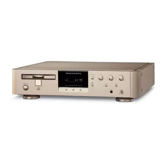
SUPER AUDIO CD PLAYER SA-17S1
SOUND MODE
TABLE OF CONTENTS
SA-17S1
SA17S1 /
Super Audio CD Player
OPEN/CLOSE
PLAY
STOP
DISPLAY
TIME
PHANTOM-C
PHONES
F1N/L1G/N1G/S1G
PAUSE
LEVEL
MIN
MAX
PAGE
R
08AK855010 MIT
First Issue 2002.12
Advertisement
Table of Contents

Related Manuals for Marantz SA17S1


Summary of Contents for Marantz SA17S1
-
Page 1: Table Of Contents
Service SA17S1 / F1N/L1G/N1G/S1G Manual Super Audio CD Player OPEN/CLOSE PLAY STOP PAUSE DISPLAY POWER ON/OFF SUPER AUDIO CD PLAYER SA-17S1 SOUND MODE TIME PHANTOM-C PHONES LEVEL TABLE OF CONTENTS SECTION PAGE 1. TECHNICAL SPECIFICATIONS ....................1 2. SERVICE MODE........................... 2 3. - Page 2 MARANTZ Parts for your equipment are generally available to our National Marantz Subsidiary or Agent. ORDERING PARTS : Parts can be ordered either by mail or by Fax.. In both cases, the correct part number has to be specifi ed.
-
Page 3: Technical Specifications
1. TECHNICAL SPECIFICATIONS Super Audio CD Audio Characteristics Analog output Channels 6channels (Max.) 2channels Frequency range 2Hz — 100kHz 2Hz — 20kHz Frequency characteristics 2Hz — 50kHz (-3dB) 2Hz — 20kHz Dynamic range 114dB 100dB THD (1kHz) 0.0008% 0.0020% Wow & Flutter Precision of quartz Precision of quartz Output level... -
Page 4: Service Mode
2. SERVICE MODE 2-1. Factory mode While pressing <OPEN/CLOSE>and<NEXT>plug in the Mains cord. "SA-17S1" is displayed Press< > Version of Backend(QF01) u-COM is displayed "Ver : X.XX" is displayed Press< > Version of Frontend(Q125) µ-COM is displayed "DrvVer : XX.XX" is displayed Press<... -
Page 5: Taking The Disc Out Of Emergency
3. TAKING THE DISC OUT OF EMERGENCY 1. Remove 8 screws on the top cover and remove the top cover. 2. Remove 6 screws on the side panel and remove the side panel. 3. Remove Power SW. Link. 4. Remove 4 screws pointed with the arrows. 5. -
Page 6: Caution Optical Pick Up And Servo Board
4. CAUTION Optical pick up and Servo Board When removing the fl at wire between Optical pick up and Servo Board (PV16), Solder the four lands pointed by arrows to short the circuit. Otherwise the LASER DIODE may be damaged by static electricity. -
Page 7: Block Diagram
5. BLOCK DIAGRAM SACD UNIT BLOCK DAC PWB TURNTABLE EM636165TS-7 M11L1616SA-45 SDRAM(16M) D-RAM(16M) photo DAPC/DARD CXD1881R L.ch DACL/LRCK HDAM SYCL L.ch HDAM HDAM RF-AMP, AGC, EQ L ch CS4397 Diffrencial AMP Laser DAPC LASER POWER CONTROL 2nd-LPF & control CXD2752R/ CXD1882R &... -
Page 8: Schematic Diagram
6. SCHEMATIC DIAGRAM JL02 JF01 EARTH WF04 FOR DAC +5VD (BUS LINE) D822 Q821 TO SERVO D803 Q801 TO SERV O NJM7808F L821 BA05T L801 11EQS10 +12V 11EQS10 +7.6V JL01 3AC9 1AC8 D821 11EQS10 D802 EARTH DIGO M-GND DIGO 4AC9 11EQS10 ACXXX D824... - Page 9 CURRENT LPF DIFFERENCIAL POWR & DAC PCB 6-CHANNEL DAC/LPF (AUDIO) Q623 Q618 2SC2240 PA16 C605 2SA970 GR,BL 470 16V GR,BL Q607 Q617 2SK170 2SA970 GR,BL Q601 Q615 2SK170 FROM 2/5 PAGE 2SK369 GR,BL Q604 Q605 Q612 Q613 2SA970 R603 2SA970 2SA970 Q619 (DAC BUS)
- Page 10 RF AMP AND ACTUTOR CONTROL C178 768F S Q108 2SK3019 D3.3CD Q103 2SB798 XMODON C169 R109 Q107 D105 D3.3DV L103 2SK3019 1SS301,DAN202U VMODE FSJP Q115 TC74LVX4053FT C179 R168 4.7k Q119 R120 J101 RFDCO DFCT DFCT EXCK TC7SHU04F 25P 1M M DFCT EXCK R169...
- Page 11 DVD DECORD CONTROL MPU DECMNT2 DECMNT2 R263 R261 JIT5V FROM Q110 C287 R295 (RF AMP) 4700p R271 100k RFAC 4.7k RFAC Q111 C288 NJM2115V R308 R306 R302 470k R267 R266 D3.3DV M3.3V C289 C284 6.8k R307 R305 R304 C285 150k 0.01 0.47 0.01...
- Page 12 RF22 QF04 RF21 AT24C04N L132 Q151 L133 J109 NJM2391DL1-33 3.3V 1A 3.3V L121 D3.3DS D5VDV Q152 L123 FCLK NJM2391DL1-33 D3.3DI 3.3V 1A FDAT D3.3DV RF04 CF08 3.3V 22/6.3 CF04 WRDAT FMD0 L122 FMD2 A3.3DV RF05 D3.3CD RF06 L126 L128 MSRST A3.3CD FMD2 R230...
- Page 13 VX01 HQ31302410 TIMER RNDM PROG A Ð B DISC TIME SACD G[6] AM32 P[32] G[5] AM31 P[31] MULTI G[4] AM30 P[30] G[3] AM29 P[29] G[2] TEXT 1 2 9 10 11 12 13 14 15 16 17 18 19 20 AM28 P[28] G[1]...
-
Page 14: Parts Location
7. PARTS LOCATION PO16 PO16 Q507 Q553 Q554 Q551 Q552 Q503 - Q501 Q504 2SK170 Q555 - Q558 Q508 - Q505 Q501 2SK369 BL Q505 Q504 2SA970 2SA970 A-GND GR,BL GR,BL -12V -12VA Q502 Q506 2SK369 BL 2SC2240 A-GND +12V +12VA GR,BL A-GND... - Page 15 PA16 QD21 - QD27 Q609 Q611 - Q616 Q617 - Q624 Q601 Q603 - Q608 Q802 QD61 Q651 Q653 - Q658 Q659 Q661 - Q666 Q667 - Q674 Q803 Q409 Q411 - Q416 Q417 - Q424 Q821 QD60 Q401 Q403 - Q408 Q801 QD41 Q451 Q453 - Q458...
- Page 16 PY16 QY05 QY01 PP16 Q853 Q857 Q851 Q855 Q852 Q856 PR16 Q904 Q908 Q912 Q903 Q907 Q902 Q906 Q905 Q901 Q911 Q915 Q910 Q914 Q916 Q909 Q913 Q941 Q942 QY62 QY61 Q831 QN23 QN22 QN21 QN33 QN32 QN31 QN43 QN42 QN04 QY63 QY64 QY65 QN06 QN05 QN02 QN01...
- Page 17 PV16 PV16 Q137 Q159 Q160 Q123 Q157 Q156 Q136 Q135 QF01 Q153 Q128 Q158 Q141 Q140 QF04 Q139 QF02 Q134 Q129 Q155 Q126 QF03 Q132 Q133 Q152 Q121 Q110 Q122 Q151 Q102 Q101 Q108 Q107 Q124 Q127 Q113 Q114 Q103 Q104 Q109 Q111 Q112 Q118...
-
Page 18: Microprocessor And Ic Data
8. MICROPROCESSOR AND IC DATA Q116 : CXD3068Q Pin Description 53 FILO Analog Master PLL fi lter output (slave = digital PLL). Symbol Description 54 FILI Master PLL fi lter input. 1 DVDD0 — Digital power supply. 55 PCO 1, Z, 0 Master PLL charge pump output. - Page 19 Q116 : CXD3068Q 5 9 6 0 1 1 1 3 6 8 6 5 6 6 7 1 7 2 TES1 TEST FSTO C l o c k E r r o r XRST G e n e r a t o r C o r r e c t o r C4 M D / A...
- Page 20 Q101 : CXD1881R Pin Description Power Supply Pins Name Type Description — Power supply pin for the RF block and serial port — Power supply pin for the servo block — Ground pin for the RF block and serial port —...
- Page 21 Analog Pins Name Type Description — The RF AGC integration capacitor CBYP, is connected between BYP and VPA. — DIFFERENTIAL PHASE TRACKING LPF PIN: The external capacitance is connected between CN. — DIFFERENTIAL PHASE TRACKING LPF PIN: The external capacitance is connected between CP. —...
- Page 22 Q123 : CXD2752R Pin Symbol I/O Description No. 1 VSC — Core GND. 2 XMSLAT Latch input for microcomputer serial communication. The address and data are atched at the fall of this pin. 3 MSCK Shift clock input for microcomputer serial communication. The serial input data is loaded and shifted at the rise of the clock input to this pin.
- Page 23 61 PHREFI Phase reference signal input for DSD output phase modulation. 62 PHREFO O Phase reference signal output for DSD output phase modulation. 63 ZDFL O Lch zero data detection fl ag (when set by the microcomputer). Goes high when silent data continues for 300ms. 64 DSAL O Lch DSD data output.
- Page 24 Q123 : CXD2752R 126 WARFI Ai Analog RF signal input for PSP physical disc mark detection. The full scale is 0.0 to 2.5V. (typ.) 127 WAVRB Ai A/D bottom reference for PSP physical disc mark detection. The voltage input to this pin is set to bottom level of the A/D converter.
- Page 25 Q123 : CXD2752R WARF I A / D WAD [ 7 : 0 ] DSARS P S P D a t a D e t e c t i o n DSAL S DSAL FE DQ [ 7 : 0 ] D S T D e c o d e r DSAC A [ 1 1 : 0 ]...
- Page 26 Q124 : CXD1882R processing mode for DVD + RW discs. For DEFECT input, an external high signal is input during the DEFECT period. Pin Description (2) APEO (absolute phase error: output) The pin descriptions by function are given below. Absolute phase error signal. It is integrated and used to evaluate the quality of the read channel.
- Page 27 5. Host Interface (31 pins) not ready to respond to a data transfer request; open drain Pin symbols are listed in the order of ATAPI mode, DMA mode signal. This is connected with the IORDY pin of the ATAPI and AV mode. Pull up means that the pin should be pulled up by a interface.
- Page 28 Q124 : CXD1882R 7 9 , 8 0 , 6 6 t o 6 9 , 7 1 , 7 3 t o 7 5 , 9 6 , 9 7 , 1 1 1 1 1 3 1 1 4 1 1 5 9 1 9 2 9 3 8 2 t o 8 7 , 8 9 9 9 , 1 0 1 , 1 0 2 , 1 0 4 t o 1 0 6...
- Page 29 Q125 : GXPQ7100(MASK) Pin No. Pin Name I/O Description 1 FTMUT Actuator driver mute signal for foc/track 2 SLMUT Actuator driver mute signal for spin/sledg 3 AMUT Muting on/off "L" : muting on for CXD3068Q 4 SMUT Muting on/off signal output to the DSD decoder "H" : muting on 5 XRST System reset signal output (L= reset) 6 CD/XDVD...
- Page 30 Q125 : GXPQ7100(MASK) 66 FJUP_D Focus jump DOWN signal output 67 FJUP_U Focus jump UP signal output 68 AVSS Ground terminal (for A/D converter) 69 AVREF Reference voltage input terminal (for A/D converter) 70 AVDD power supply terminal (+3.3V) (for A/D converter) 71 XFCMP_L Layer swicthing monitor signal at the down from refrenc level 72 XFCMP_H...
- Page 31 QD41/QD61/QD71 : CS4397 Reset - RST The Left/Right clock determines which channel is currently being Pin 1, Input input on the serial audio data input, Function: SDATA. The frequency of the Left/Right clock must be at the input The device enters a low power mode and all internal state sample rate.
- Page 32 QD41/QD61/QD71 : CS4397 Analog Ground - AGND required relationship between the Left/Right clock, serial clock Pins 18 and 21, Inputs and serial data as detailed in Figures 29-33 Selection of the standard 15 µs/50 µs digital de-emphasis fi lter response, Figure Function: Analog ground reference.
- Page 33 QF01 : MB90F553A Pin Port Signal Function Description Active Pin Port Signal Function Description Active 1 P20/A16 DAC select Front L/R Active H 51 MD2 MODE3 Mode select Norma L 2 P21/A17 DAC select Surround L/R Active H 52 HST HWSTBY Hardware standby Normal H...
-
Page 34: Exploded View And Parts List
9. EXPLODED VIEW AND PARTS LIST 5 4 0 5 0 0 5 Dx 8 3 ( M) 0 0 4 Dx 8 5 1 2 9 5 1 2 8 3 X 8 ( M) 3 X 8 ( M) W 0 0 1 N ONL Y 0 0 2 Dx 8... - Page 35 1MM-PITCH 17P 002S CUSHION FOR SET LEFT 410K809020 WF08 JUMPER LEAD J104-TRAY FFC YU06060520 003S CUSHION FOR SET RIGHT 08AK809030 1.25MM-PITCH 6P 009S CUSHION FOR SET NOTE : "nsp" PART IS LISTED FOR REFERENCE ONLY, MARANTZ WILL NOT SUPPLY THESE PARTS.
-
Page 36: Mecha Loader Ass'y
01AK163010 TRAY 62-218-1016 01AK004010 CLAMPER-2 62-223-3041 YOKE 56-119-4030 62-070-3018 CONNECTOR 6FESTVKN *SM000380R LEVER SWITCH F501-0012 SCREW GSP14A25027 SCREW 03-300-4525 01AK264010 BELT LOADING 02-084228 WASHER GWP52X100025 NOTE : "nsp" PART IS LISTED FOR REFERENCE ONLY, MARANTZ WILL NOT SUPPLY THESE PARTS. -
Page 37: Electrical Parts List
11. ELECTRICAL PARTS LIST NOTE ON SAFETY FOR FUSIBLE RESISTOR : ASSIGNMENT OF COMMON PARTS CODES. RESISTORS The suppliers and their type numbers of fusible resistors : 1) GD05 × × × 140, Carbon film fixed resistor, ±5% 1/4W are as follows; : 2) GD05 ×... - Page 38 R701-R714 R722-R741 R743 R744 C702 /N OF55331550 FILM 330pF 100V OF55331550 R751-R764 R772-R791 R793 R794 C704 /F/L/S FILM 120pF J 100V APSV OF15121540 R801-R803 RD22-RD25 RD27 NOTE : "nsp" PART IS LISTED FOR REFERENCE ONLY, MARANTZ WILL NOT SUPPLY THESE PARTS.
- Page 39 HT109702A0 Q717 HT109702A0 TRS. 2SA970 GR OR BL HT109702A0 Q464 HT322402A0 TRS. 2SC2240 GR OR BL HT322402A0 Q718 HT109702A0 TRS. 2SA970 GR OR BL HT109702A0 NOTE : "nsp" PART IS LISTED FOR REFERENCE ONLY, MARANTZ WILL NOT SUPPLY THESE PARTS.
- Page 40 ELECT. 470µF M 35V RA-2 OA47703520 LT02 FC90050130 FERRITE BEAD BL02RN2-R62T2 FC90050130 C832 ELECT. 10µF 63V RA-2 OA10606320 C851 OB47803520 ELECT. CAP 4700µF M 35V OB47803520 FOR HIFI NOTE : "nsp" PART IS LISTED FOR REFERENCE ONLY, MARANTZ WILL NOT SUPPLY THESE PARTS.
- Page 41 HT10001000 TRS. A1048 A933S A1267 ETC. HT10001000 C112 CER. CHIP 1000pF ±10% B 50V DK96102300 QY61 HT10001000 TRS. A1048 A933S A1267 ETC. HT10001000 C113 EY10601620 TANTL. CHIP 10µF 16V EY10601620 NOTE : "nsp" PART IS LISTED FOR REFERENCE ONLY, MARANTZ WILL NOT SUPPLY THESE PARTS.
- Page 42 EY22600620 TANTL. CHIP 22µF 6.3V EY22600620 C183 CER. CHIP 0.1µF GRM39F104Z16 DK98104200 C259 CER. CHIP 1µF 10V F DK98105200 C184 CER. CHIP 1µF 10V F DK98105200 NOTE : "nsp" PART IS LISTED FOR REFERENCE ONLY, MARANTZ WILL NOT SUPPLY THESE PARTS.
- Page 43 EY47501050 R155 CHIP 330kΩ ±5% 1/16W NN05334610 C363 CER. CHIP 0.1µF 16V DK96104200 R156 CHIP 10kΩ ±5% 1/16W NN05103610 R157 CHIP 1.5kΩ ±5% 1/16W NN05152610 NOTE : "nsp" PART IS LISTED FOR REFERENCE ONLY, MARANTZ WILL NOT SUPPLY THESE PARTS.
- Page 44 R343 CHIP 2.2kΩ ±5% 1/16W NN05222610 R229 CHIP MCR03EZHUJ202 NN05202610 R344 CHIP 10kΩ ±5% 1/16W NN05103610 2120 108 92178 R347 CHIP 0Ω ±5% 1/16W NN05000610 NOTE : "nsp" PART IS LISTED FOR REFERENCE ONLY, MARANTZ WILL NOT SUPPLY THESE PARTS.
- Page 45 HU01AKY10F MICROPROCESSOR CXPQ71000 HU01AKY10F CONTROL-UPC PY16-SEMICONDUCTORS Q126 HC005805K0 IC TC74VHC157FT HC005805K0 DY04 HI10062320 L.E.D. LT3D8B RED 3O HI10062320 QY01 HC10416030 IC FL DRIVER LC75712E HC10416030 NOTE : "nsp" PART IS LISTED FOR REFERENCE ONLY, MARANTZ WILL NOT SUPPLY THESE PARTS.
- Page 46 PY16-MISCELLANEOUS SY01 SP01012030 PUSH SWITCH SP01012030 SY10 SKHVBF 260GF RED VX01 HQ31301920 DISPLAY UNIT FTD CM2059C HQ31301920 ZY01 HW10004210 PHOTO UNIT RPM6936-V4 HW10004210 IR SENSOR NOTE : "nsp" PART IS LISTED FOR REFERENCE ONLY, MARANTZ WILL NOT SUPPLY THESE PARTS.
Need help?
Do you have a question about the SA17S1 and is the answer not in the manual?
Questions and answers