Table of Contents
Advertisement
Service
Manual
STANDBY
POWER
SECTION
1. TECHNICAL SPECIFICATIONS ................................................................................................... 1
2. SERVICE MODE........................................................................................................................... 2
3. TAKING THE DISC OUT OF EMERGENCY ................................................................................. 3
4. CAUTION Optical pick up and Servo Board.................................................................................. 4
5. BLOCK DIAGRAM ........................................................................................................................ 5
6. SCHEMATIC DIAGRAM................................................................................................................ 7
7. PARTS LOCATION...................................................................................................................... 20
8. MICROPROCESSOR AND IC DATA........................................................................................... 27
9. EXPLODED VIEW AND PARTS LIST ......................................................................................... 45
10. LOADING MECHANISM ASS'Y .................................................................................................. 48
11. ELECTRICAL PARTS LIST ......................................................................................................... 49
Please use this service manual with referring to the user guide ( D.F.U. ) without fail.
Printed on 100% Recycled Paper
Printed in Japan
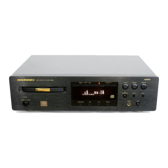
SUPER AUDIO CD PLAYER SA8260
ON/STANDBY
TABLE OF CONTENTS
SA8260
SA8260 /
Super Audio CD Player
STEREO
SACD
MULTI
CD
DISPLAY OFF
PLAY
OPEN/CLOSE
PHONES
SOUND MODE
TIME
TEXT
DISPLAY
F1N/S1G/U1G
F1B/S1B/U1B
STOP
PAUSE
/
/
LEVEL
-
+
PAGE
R
01AK855010 MIT
First Issue 2002.04
Advertisement
Table of Contents

Related Manuals for Marantz SA8260/F1N


Summary of Contents for Marantz SA8260/F1N
- Page 1 Service SA8260 / F1N/S1G/U1G F1B/S1B/U1B Manual Super Audio CD Player SUPER AUDIO CD PLAYER SA8260 STEREO SACD MULTI DISPLAY OFF PLAY STOP PAUSE OPEN/CLOSE STANDBY POWER ON/STANDBY PHONES LEVEL SOUND MODE TIME TEXT DISPLAY TABLE OF CONTENTS SECTION PAGE 1. TECHNICAL SPECIFICATIONS ....................1 2.
- Page 2 Parts for your MARANTZ equipment are generally available to our National Marantz Subsidiary or Agent. ORDERING PARTS : Parts can be ordered either by mail or by Fax.. In both cases, the correct part number has to be specifi ed.
-
Page 3: Technical Specifications
1. TECHNICAL SPECIFICATIONS Super Audio CD Audio Characteristics Analog output Channels 6channels (Max.) 2channels Frequency range 2Hz — 100kHz 2Hz — 20kHz Frequency characteristics 2Hz — 50kHz (-3dB) 2Hz — 20kHz Dynamic range 113dB 100dB THD (1kHz) 0.0015% 0.0020% wow & fl utter Precision of quartz Precision of quartz Output level... -
Page 4: Service Mode
2. SERVICE MODE While pressing <OPEN/CLOSE>and<NEXT>plug in the Mains cord. "SA8260" is displayed Press< > Version of Backend(QF01) u-COM is displayed "Ver : X.XX" is displayed Press< > Version of Frontend(Q125) u-COM is displayed "DrvVer : XX.XX" is displayed Press< >... -
Page 5: Taking The Disc Out Of Emergency
3. TAKING THE DISC OUT OF EMERGENCY 1. Remove 6 screws on the top cover and remove the top cover. 2. Remove 4 screws pointed with the arrows. 3. Disconnect all the wires at the right and rear side. 4. Remove the Mecha. component. 5. -
Page 6: Caution Optical Pick Up And Servo Board
4. CAUTION Optical pick up and Servo Board When removing the fl at wire between Optical pick up and Servo Board (PV16), Solder the four lands pointed by arrows to short the circuit. Otherwise the LASER DIODE may be damaged by static electricity. -
Page 7: Block Diagram
5. BLOCK DIAGRAM RNDMPROG A – B RPT 1 TIME TEXT 1 2 9 10 1112 1314 1516 1718 1920... -
Page 8: Schematic Diagram
6. SCHEMATIC DIAGRAM PP16 MAIN POWER AND MUTING/FILTER-SW JL02 EARTH FOR DAC JF01 (BUS LINE) WF04 BK12V JL01 EARTH JF04 ACXXX WF06 DIGO M-GND DIGO ACXXX RC5S RC5S BK5V BK5V 5.6VA BK5V TO SERVO STBSW STBSW 5.6VA CDLED CDLED Q821 VREF VREF D822... - Page 9 DIFFERENCIAL CURRENT LPF 031G HDAM SHILED 2-CHANNEL DAC/LPF (AUDIO) Q623 Q618 2SC2240 2SA970 GR,BL FROM X/X PAGE GR,BL Q607 Q617 (DAC BUS) 2SK170 2SA970 GR,BL Q615 Q601 2SK170 2SK369 BL Q605 Q604 Q612 Q613 2SA970 R603 2SA970 2SA970 Q619 GR,BL 2SA970 GR,BL GR,BL...
- Page 10 RF AMP AND ACTUTOR CONTROL C178 768F S Q108 2SK3019 D3.3CD Q103 2SB798 XMODON C169 R109 Q107 D105 D3.3DV L103 2SK3019 1SS301,DAN202U VMODE FSJP Q115 TC74LVX4053FT C179 R168 4.7k Q119 R120 J101 RFDCO DFCT DFCT EXCK TC7SHU04F 25P 1M M DFCT EXCK R169...
- Page 11 DVD DECORD CONTROL MPU DECMNT2 DECMNT2 R263 R261 JIT5V FROM Q110 C287 R295 (RF AMP) 4700p R271 100k RFAC 4.7k RFAC Q111 C288 NJM2115V R308 R306 R302 470k R267 R266 D3.3DV M3.3V C289 C284 6.8k R307 R305 R304 C285 150k 0.01 0.47 0.01...
- Page 12 RF22 QF04 RF21 AT24C04N L132 Q151 L133 J109 NJM2391DL1-33 3.3V 1A 3.3V L121 D3.3DS L131 D5VDV Q152 L123 FCLK NJM2391DL1-33 D3.3DI L130 3.3V 1A FDAT D3.3DV RF04 CF08 3.3V 22/6.3 CF04 WRDAT FMD0 L122 FMD2 A3.3DV RF05 D3.3CD RF06 L126 L128 MSRST A3.3CD...
- Page 13 4.3V VX01 HQ31302410 RNDMPROG A – B RPT 1 TIME TEXT 1 2 9 10 1112 1314 1516 1718 1920 9 10 11 12 13 14 15 16 17 18 19 20 21 22 23 24 25 26 27 28 29 30 31 32 33 34 35 36 37 38 39 40 41 42 43 44 45 CY02 47/16V CY01...
-
Page 14: Parts Location
7. PARTS LOCATION PR16 HEADPHONE PA16 R907 C903 1.5K Q903 220/16V 2SC2120 D901 R919 A-GND 1SS176 R903 R911 C905 Q909 47/16V 2SC2878 R921 NJM2114 4.7K R905 R925 R913 R917 4.7K Q901 A-GND D903 1SS176 Q905 A-GND A-GND 2SA950 QN71 - QN74 QN41 - QN44 J902 R901... - Page 15 PP16 QF51 QN71 - QN74 QF52 QT01 Q857 Q723 Q724 Q773 Q774 Q855 Q856 Q721 Q771 Q852 Q715 Q765 Q851 Q853 Q714 Q764 Q709 Q769 Q821 QY05 QY61 Q708 Q758 QN12 QN04 QN01 QN11 QN02 QN03 Q801 Q802 Q701 Q751 Q802 QD23 QD21...
- Page 16 PY16 QY05 QY02 QY04 QY03 QY06 QY01 PY26 PH16 QH03 QH02 QH01 PH26 PR16 Q909 Q907 Q901 Q910 Q908 Q903 Q905 Q906 Q904...
- Page 17 PV16 PV16 Q137 Q159 Q160 Q123 Q157 Q156 Q136 Q135 QF01 Q153 Q117 Q116 Q119 Q139 QF02 Q118 Q134 Q132 Q133 Q113 Q114 Q127 Q121 Q110 Q102 Q101 Q108 Q107 Q124 Q152 Q151 Q122 Q103 Q104 Q109 QF03 Q126 Q155 Q129 Q125 QF04 Q104...
-
Page 18: Microprocessor And Ic Data
8. MICROPROCESSOR AND IC DATA 53 FILO Analog Master PLL fi lter output (slave = digital PLL). 54 FILI Master PLL fi lter input. Q116 : CXD3068Q 55 PCO 1, Z, 0 Master PLL charge pump output. Pin Description 56 AVDD1 —... - Page 19 Q116 : CXD3068Q 5 9 6 0 1 1 1 3 6 8 6 5 6 6 7 1 7 2 TES1 TEST FSTO C l o c k E r r o r XRST G e n e r a t o r C o r r e c t o r C4 M D / A...
- Page 20 Q101 : CXD1881R Pin Description Power Supply Pins Name Type Description — Power supply pin for the RF block and serial port — Power supply pin for the servo block — Ground pin for the RF block and serial port —...
- Page 21 Analog Pins Name Type Description — The RF AGC integration capacitor CBYP, is connected between BYP and VPA. — DIFFERENTIAL PHASE TRACKING LPF PIN: The external capacitance is connected between CN. — DIFFERENTIAL PHASE TRACKING LPF PIN: The external capacitance is connected between CP. —...
- Page 22 Q123 : CXD2752R Pin Symbol I/O Description No. 1 VSC — Core GND. 2 XMSLAT Latch input for microcomputer serial communication. The address and data are atched at the fall of this pin. 3 MSCK Shift clock input for microcomputer serial communication. The serial input data is loaded and shifted at the rise of the clock input to this pin.
- Page 23 61 PHREFI Phase reference signal input for DSD output phase modulation. 62 PHREFO O Phase reference signal output for DSD output phase modulation. 63 ZDFL O Lch zero data detection fl ag (when set by the microcomputer). Goes high when silent data continues for 300ms. 64 DSAL O Lch DSD data output.
- Page 24 Q123 : CXD2752R 126 WARFI Ai Analog RF signal input for PSP physical disc mark detection. The full scale is 0.0 to 2.5V. (typ.) 127 WAVRB Ai A/D bottom reference for PSP physical disc mark detection. The voltage input to this pin is set to bottom level of the A/D converter.
- Page 25 Q123 : CXD2752R WARF I A / D WAD [ 7 : 0 ] DSARS P S P D a t a D e t e c t i o n DSAL S DSAL FE DQ [ 7 : 0 ] D S T D e c o d e r DSAC A [ 1 1 : 0 ]...
- Page 26 Q124 : CXD1882R processing mode for DVD + RW discs. For DEFECT input, an external high signal is input during the DEFECT period. Pin Description (2) APEO (absolute phase error: output) The pin descriptions by function are given below. Absolute phase error signal. It is integrated and used to evaluate the quality of the read channel.
- Page 27 5. Host Interface (31 pins) not ready to respond to a data transfer request; open drain Pin symbols are listed in the order of ATAPI mode, DMA mode signal. This is connected with the IORDY pin of the ATAPI and AV mode. Pull up means that the pin should be pulled up by a interface.
- Page 28 Q124 : CXD1882R 7 9 , 8 0 , 6 6 t o 6 9 , 7 1 , 7 3 t o 7 5 , 9 6 , 9 7 , 1 1 1 1 1 3 1 1 4 1 1 5 9 1 9 2 9 3 8 2 t o 8 7 , 8 9 9 9 , 1 0 1 , 1 0 2 , 1 0 4 t o 1 0 6...
- Page 29 Q125 : CXP973064R-1(FLASH) / GXPQ7100(MASK) Pin No. Pin Name I/O Description 1 FTMUT Actuator driver mute signal for foc/track 2 SLMUT Actuator driver mute signal for spin/sledg 3 AMUT Muting on/off "L" : muting on for CXD3068Q 4 SMUT Muting on/off signal output to the DSD decoder "H" : muting on 5 XRST System reset signal output (L= reset) 6 CD/XDVD...
- Page 30 Q125 : CXP973064R-1(FLASH) / GXPQ7100(MASK) 66 FJUP_D Focus jump DOWN signal output 67 FJUP_U Focus jump UP signal output 68 AVSS Ground terminal (for A/D converter) 69 AVREF Reference voltage input terminal (for A/D converter) 70 AVDD power supply terminal (+3.3V) (for A/D converter) 71 XFCMP_L Layer swicthing monitor signal at the down from refrenc level 72 XFCMP_H...
- Page 31 QD41/QD61 : CS4397 Reset - RST The Left/Right clock determines which channel is currently being Pin 1, Input input on the serial audio data input, Function: SDATA. The frequency of the Left/Right clock must be at the input The device enters a low power mode and all internal state sample rate.
- Page 32 QD41/QD61 : CS4397 Analog Ground - AGND required relationship between the Left/Right clock, serial clock Pins 18 and 21, Inputs and serial data as detailed in Figures 29-33 Selection of the standard 15 µs/50 µs digital de-emphasis fi lter response, Figure Function: Analog ground reference.
- Page 33 QF01 : MB90F553A 50 MD1 MODE2 Mode select Normal=H Port Signal Function Description Active 51 MD2 MODE3 Mode select Normal=L 1 P20/A16 DAC select Front L/R active H 52 HST HWSTBY Hardware standby Normal=H 2 P21/A17 DAC select Surround L/R active H 53 P72/IRQ2 SEEK...
-
Page 34: Exploded View And Parts List
9. EXPLODED VIEW AND PARTS LIST 5 1 2 6 3 X 8 ( M) W0 0 1 5 1 2 6 3 X 8 ( M) x 2 5 1 2 8 3 X 8 ( M) J 0 0 1 9 0 1 G L 0 0 2 5 1 2 8... - Page 35 MAINS CORD FOR UK ZC01804100 CINCH ST.CORD 1M GOLD AC 250V 10A W001 /U1 MAINS CORD UL/CSA ZC01803100 10A 125V W101 FFC J101-OPT_UNIT 1MM 25P YU25080550 NOTE : "nsp" PART IS LISTED FOR REFERENCE ONLY, MARANTZ WILL NOT SUPPLY THESE PARTS.
-
Page 36: Loading Mechanism Ass'y
01AK163010 TRAY 62-218-1016 01AK004010 CLAMPER-2 62-223-3041 YOKE 56-119-4030 62-070-3018 CONNECTOR 6FESTVKN *SM000380R LEVER SWITCH F501-0012 SCREW GSP14A25027 SCREW 03-300-4525 01AK264010 BELT LOADING 02-084228 WASHER GWP52X100025 NOTE : "nsp" PART IS LISTED FOR REFERENCE ONLY, MARANTZ WILL NOT SUPPLY THESE PARTS. -
Page 37: Electrical Parts List
11. ELECTRICAL PARTS LIST NOTE ON SAFETY FOR FUSIBLE RESISTOR : ASSIGNMENT OF COMMON PARTS CODES. RESISTORS The suppliers and their type numbers of fusible resistors : 1) GD05 × × × 140, Carbon film fixed resistor, ±5% 1/4W are as follows; : 2) GD05 ×... - Page 38 9965 000 04966 FILM 1200pF TP 100V PP OF15122540 Q419 4822 130 42949 TRS. 2SA970 GR OR BL HT109702A0 C760 FILM 560pF TP 100V PP OF15561540 NOTE : "nsp" PART IS LISTED FOR REFERENCE ONLY, MARANTZ WILL NOT SUPPLY THESE PARTS.
- Page 39 4822 130 43233 TRS. 2SC2240 GR OR BL HT322402A0 Q757 5322 130 41844 F.E.T. 2SK170 V LANK HF201701H0 Q758 4822 130 62649 F.E.T. 2SJ74 V LANK HF100741H0 NOTE : "nsp" PART IS LISTED FOR REFERENCE ONLY, MARANTZ WILL NOT SUPPLY THESE PARTS.
- Page 40 ZENER DIODE HZ6L 3 6.2V HD30021010 D858 4822 130 32362 DIODE 1SS176 MA165 1SS254 HD20002000 C801 4822 124 22243 ELECT. 6800µF 16V RA-2 OA68801620 30V 0.1A NOTE : "nsp" PART IS LISTED FOR REFERENCE ONLY, MARANTZ WILL NOT SUPPLY THESE PARTS.
- Page 41 TRS. 2SA970 GR OR BL HT109702A0 LT01 4822 142 60422 PULSE TRANSF. TP41042030 TPS247MN-0386AN Q651 4822 130 42839 F.E.T. HF203691B0 LT02 FERRITE BEAD FC90050130 2SK369 BL VGDS-40V PD0.4W BL02RN2-R62T2 NOTE : "nsp" PART IS LISTED FOR REFERENCE ONLY, MARANTZ WILL NOT SUPPLY THESE PARTS.
- Page 42 4822 124 11226 TANTL CHIP 22µF 6.3V EY22600620 C104 4822 126 11687 CER. 0.1µF GRM39F104Z16 DK98104200 C175 4822 124 11226 TANTL CHIP 22µF 6.3V EY22600620 NOTE : "nsp" PART IS LISTED FOR REFERENCE ONLY, MARANTZ WILL NOT SUPPLY THESE PARTS.
- Page 43 4822 124 10772 TANTL CHIP 100µF 6.3V EY10700620 C251 4822 124 11226 TANTL CHIP 22µF 6.3V EY22600620 C346 4822 126 11687 CER. 0.1µF GRM39F104Z16 DK98104200 NOTE : "nsp" PART IS LISTED FOR REFERENCE ONLY, MARANTZ WILL NOT SUPPLY THESE PARTS.
- Page 44 4822 051 30563 CHIP 56kΩ ±5% 1/16W NN05563610 R143 4822 051 30332 CHIP 3.3kΩ ±5% 1/16W NN05332610 R216 4822 051 30473 CHIP 47kΩ ±5% 1/16W NN05473610 NOTE : "nsp" PART IS LISTED FOR REFERENCE ONLY, MARANTZ WILL NOT SUPPLY THESE PARTS.
- Page 45 NN05223610 DVD DECORDER R311 4822 051 30473 CHIP 47k ±5% 1/16W NN05473610 Q125 MICROPROCESSOR HU01AKY100 R312 4822 051 30102 CHIP ±5% 1/16W NN05102610 CXPQ71000 CONTROL-UPC NOTE : "nsp" PART IS LISTED FOR REFERENCE ONLY, MARANTZ WILL NOT SUPPLY THESE PARTS.
- Page 46 FERRITE CORE FC90020100 FB M J2125HM330-T XF01 CERAMIC VIB. FQ08004070 CSTCC8.00MG-TC 8.000MHz X101 CRYSTAL XTAL 33.8688MHz JX33001470 X103 CERAMIC VIB. FQ02005060 CSTCW-X SMD TYPE 20.0MHz NOTE : "nsp" PART IS LISTED FOR REFERENCE ONLY, MARANTZ WILL NOT SUPPLY THESE PARTS.
Need help?
Do you have a question about the SA8260/F1N and is the answer not in the manual?
Questions and answers