Table of Contents
Advertisement
Quick Links
UM10340_5
TFA9879 digital input mono Class-D amplifier demo PCB
Rev. 05 — 30 aug. 2011
Document information
Info
Content
Keywords
Class-D amplifier, Digital input, High efficiency, Filter free
Abstract
This User Manual describes the TFA9879 digital input mono Class-D
demonstration PCB based on NXP Semiconductors' TFA9879 filter-free
mono BTL Class-D audio amplifier device. The TFA9879 device is
intended for portable applications that support a digital output, which is
less sensitive to external RF fields. The low power consumption will
increase the battery life and an excellent audio performance with high
PSRR is achieved by the integrated feedback loop.
Furthermore the device is very robust due to the integrated protections
like OCP, OTP and several input protections.
The demonstration PCB is designed to operate from a single supply with
a wide supply voltage range of 2.5V...5.5V delivering an output power up
to 1.6W
the TFA9879 is very small because only three external components are
required. The demo board is EMC compliant and contains 15kV ESD
protections at the speaker output.
Ω
in 8
BTL or 2.7W
RMS
RMS
User manual
Ω
4
BTL. The application PCB area for
Advertisement
Table of Contents

Subscribe to Our Youtube Channel
Related Manuals for NXP Semiconductors UM10340-5


Summary of Contents for NXP Semiconductors UM10340-5
- Page 1 Abstract This User Manual describes the TFA9879 digital input mono Class-D demonstration PCB based on NXP Semiconductors’ TFA9879 filter-free mono BTL Class-D audio amplifier device. The TFA9879 device is intended for portable applications that support a digital output, which is less sensitive to external RF fields.
-
Page 2: Contact Information
UM10340_5 NXP Semiconductors TFA9879 demonstration PCB Revision history Date Description 20090227 Initial version 20090806 Main PCB updated to revision 2 and WLCSP translation PCB replaced by HVQFN24 translation PCB 20090911 Translation PCB updated to revision 3 for TFA9879 (N1B2/N1C) engineering samples... -
Page 3: Introduction
1. Introduction This User Manual describes the TFA9879 digital input mono Class-D amplifier demonstration PCB based on NXP Semiconductors’ TFA9879HN device. Extension “HN” is referring to the HVQFN24 package dedicated for reflow soldering. The TFA9879 demonstration PCB is designed in such a way that it is easy to operate the TFA9879 device for demonstration purposes and for validation. - Page 4 UM10340_5 NXP Semiconductors TFA9879 demonstration PCB The necessary information is given for a quick start-up of the demonstration PCB (see paragraph 2). Paragraph 3 shows the results of the audio characterization and the schematic, BOM and layout is provided in paragraph 4, 5 and 6.
-
Page 5: Setup Demonstration Pcb
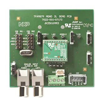
UM10340_5 NXP Semiconductors TFA9879 demonstration PCB 2. Setup demonstration PCB 2.1 Hardware setup Figure 2 is showing the hardware setup of the TFA9879 mono demonstration PCB with screw terminals for connecting the power supply (X3) and the speaker cables (X7). -
Page 6: Pcb Switch Settings
UM10340_5 NXP Semiconductors TFA9879 demonstration PCB REF TYPE Label Description 4, 6, 8 Ground LRCK1 Word clock input 1 SCK1 Bit clock input 1 Header, double row 1, 2, 9, 10 Not connected SDI2 Data input 2 4, 6, 8... -
Page 7: Speaker Dummy Load
UM10340_5 NXP Semiconductors TFA9879 demonstration PCB 2.1.3 Speaker dummy load The TFA9879 is a filter-free Class-D amplifier that will directly drive the loudspeaker. For realistic measurement at a filter-free Class-D amplifier a dummy load, consisting out of a resistor (R ) in series with an inductor (L ), should replace the loudspeaker. -
Page 8: Software Setup (Gui)
UM10340_5 NXP Semiconductors TFA9879 demonstration PCB 2.2 Software setup (GUI) The TFA9879 is controlled via I2C. The Graphic User Interface (GUI) software (including USM drivers), which are supplied by the demonstration PCB, enable easy control of the I2C registers in the TFA9879. -
Page 9: Settings To Play Audio
UM10340_5 NXP Semiconductors TFA9879 demonstration PCB 7. Select a device address (D8, DA, DC or DE) from the GUI (top right side). The installation of I2C GUI is finalized and the indicator of the I2C communication should be green. Figure 7: GUI communication If the indication is still red the following should be checked: •... - Page 10 UM10340_5 NXP Semiconductors TFA9879 demonstration PCB GUI settings: • Select Powerup • Select input 2 • Select Operating Mode “On” • Increase volume (for example to 0dB) Figure 8: GUI settings to play audio © NXP B.V. 2011. All rights reserved.
-
Page 11: Performance Characterization Tfa9879Hn
UM10340_5 NXP Semiconductors TFA9879 demonstration PCB 3. Performance characterization TFA9879HN Table below shows the measured performance figures of the TFA9879HN demonstration PCB. Digital I2S input signal is applied to connector X4 and the audio analyzer is connected via an AUX-0025 passive filter from Audio Precision to the PWM outputs (OUTA, OUTB). - Page 12 UM10340_5 NXP Semiconductors TFA9879 demonstration PCB Symbol Parameters Conditions / Notes Unit Supply current total Power down mode application µA LDO off, DCDC off, ADC off LDO on, DCDC on, ADC on Off mode LDO on, DCDC off, ADC off...
-
Page 13: Schematics
UM10340_5 NXP Semiconductors TFA9879 demonstration PCB 4. Schematics © NXP B.V. 2011. All rights reserved. User manual Rev. 05 — 30 aug. 2011 13 of 20... - Page 14 UM10340_5 NXP Semiconductors TFA9879 demonstration PCB © NXP B.V. 2011. All rights reserved. User manual Rev. 05 — 30 aug. 2011 14 of 20...
-
Page 15: Bill Of Materials
UM10340_5 NXP Semiconductors TFA9879 demonstration PCB 5. Bill Of Materials 5.1 Main PCB 7022-001-07164 Item Qty Reference Part Foot print ADP3336 MSOP8 LTC3440EMS MSOP10 UDA1361TS SSOP16-SOT369-1 C1,C21 C0603 C2,C9,C11,C14 10uF C0603 C3,C12,C17,C20 C0603 C4,C5,C6,C7,C10 C0603 150pF C0603 100nF C0603 47uF... -
Page 16: Translation Pcb 7022-001-07203
UM10340_5 NXP Semiconductors TFA9879 demonstration PCB 5.2 Translation PCB 7022-001-07203 Item Reference Part Foot print TFA9879HN HVQFN24-SOT616-1 C0603 C2,C3 100n C0402 X1,X2 Header Single Row / 10p 2mm X4,X5,X6 SMD-TESTPAD-1MM5 0 Ω R0402 © NXP B.V. 2011. All rights reserved. -
Page 17: Pcb Layout
UM10340_5 NXP Semiconductors TFA9879 demonstration PCB 6. PCB layout 6.1 Main PCB 7022-001-07174 Two layer PCB (74mm x 65mm), 35µm copper and FR4 base material. Figure 9 Copper and silkscreen top layer (top view) Figure 10: Copper and silkscreen top layer (top view) ©... -
Page 18: Translation Pcb 7022-001-07213
UM10340_5 NXP Semiconductors TFA9879 demonstration PCB 6.2 Translation PCB 7022-001-07213 Two layer PCB (20mm x 18mm), 35µm copper and FR4 base material. Figure 9: Copper and silkscreen top layer (top view) Figure 10: Copper and silkscreen bottom layer (top view) ©... -
Page 19: Legal Information
Notice: All referenced brands, product names, service names and trademarks are property of their respective owners. Right to make changes — NXP Semiconductors reserves the right to make changes to information published in this document, including without limitation specifications and product descriptions, at any time and without notice. -
Page 20: Table Of Contents
UM10340_5 NXP Semiconductors TFA9879 demonstration PCB 8. Contents Main PCB 7022-001-07164 ......15 Introduction ............3 Translation PCB 7022-001-07203 ....16 Setup demonstration PCB ........5 PCB layout ............17 Hardware setup ..........5 Main PCB 7022-001-07174 ......17 2.1.1 PCB switch settings ...........
Need help?
Do you have a question about the UM10340-5 and is the answer not in the manual?
Questions and answers