Table of Contents
Advertisement
DVD AV RECEIVER
AVH-P4100DVD
DVD RDS AV RECEIVER
AVH-P4100DVD
AVH-P4100DVD
This service manual should be used together with the following manual(s):
Model No.
Order No.
CX-3250
CRT4300
DTS and DTS Digital Out are registered trademartks and the DTS logos and Symbol are
trademarks of DTS, Inc.
Manufactured under license from Dolby Laboratories. Dolby, Pro Logic, and the double-D
symbol are trademarks of Dolby Laboratories.
For details, refer to "Important Check Points for Good Servicing".
PIONEER CORPORATION
PIONEER ELECTRONICS (USA) INC. P.O. Box 1760, Long Beach, CA 90801-1760, U.S.A.
PIONEER EUROPE NV Haven 1087, Keetberglaan 1, 9120 Melsele, Belgium
PIONEER ELECTRONICS ASIACENTRE PTE. LTD. 253 Alexandra Road, #04-01, Singapore 159936
PIONEER CORPORATION 2009
Mech.Module
LS1
DVD Mech. Module : Circuit Descriptions, Mech. Descriptions, Disassembly
4-1, Meguro 1-chome, Meguro-ku, Tokyo 153-8654, Japan
AVH-P4100DVD/XN/UC
/XNEW5
/XNUW5
Remarks
ORDER NO.
CRT4275
/XN/UC
K-ZZZ. JAN. 2009 Printed in Japan
Advertisement
Table of Contents

Related Manuals for Pioneer AVH-P4100DVD/XNEW5


Summary of Contents for Pioneer AVH-P4100DVD/XNEW5
- Page 1 PIONEER CORPORATION 4-1, Meguro 1-chome, Meguro-ku, Tokyo 153-8654, Japan PIONEER ELECTRONICS (USA) INC. P.O. Box 1760, Long Beach, CA 90801-1760, U.S.A. PIONEER EUROPE NV Haven 1087, Keetberglaan 1, 9120 Melsele, Belgium PIONEER ELECTRONICS ASIACENTRE PTE. LTD. 253 Alexandra Road, #04-01, Singapore 159936 PIONEER CORPORATION 2009 K-ZZZ.
-
Page 2: Safety Information
SAFETY INFORMATION CAUTION This service manual is intended for qualified service technicians; it is not meant for the casual do-it-yourselfer. Qualified technicians have the necessary test equipment and tools, and have been trained to properly and safety repair complex products such as those covered by this manual. Improperly performed repairs can adversely affect the safety and reliability of the product and may void the warranty. - Page 3 WARNING! The AEL (accessible emission level )of the laser power output is less than CLASS 1 but the laser component is capable of emitting radiation exceeding the limit for CLASS 1. A specially instructed person should do servicing operation of the apparatus. Laser diode characteristics Wave length: DVD:660 nm to 670 nm...
- Page 4 [Important Check Points for Good Servicing] In this manual, procedures that must be performed during repairs are marked with the below symbol. Please be sure to confirm and follow these procedures. 1. Product safety Please conform to product regulations (such as safety and radiation regulations), and maintain a safe servicing environment by following the safety instructions described in this manual.
-
Page 5: Table Of Contents
8.2 MONITOR UNIT ADJUSTMENT ......................113 8.3 PCL OUTPUT CONFIRMATION ......................116 9. EXPLODED VIEWS AND PARTS LIST ......................117 9.1 PACKING(AVH-P4100DVD/XN/UC) ....................... 118 9.2 PACKING(AVH-P4100DVD/XNEW5, XNUW5) ..................120 9.3 EXTERIOR(1) ............................122 9.4 EXTERIOR(2) ............................124 9.5 EXTERIOR(3) ............................126 9.6 DVD MECHANISM MODULE.........................128 10. -
Page 6: Service Precautions
1. SERVICE PRECAUTIONS 1.1 SERVICE PRECAUTIONS 1. You should conform to the regulations governing the product (safety, radio and noise, and other regulations), and should keep the safety during servicing by following the safety instructions described in this manual. 2. Be careful in handling ICs. Some ICs such as MOS type are so fragile that they can be damaged by electrostatic induction. -
Page 7: Notes On Soldering
1.2 NOTES ON SOLDERING For environmental protection, lead-free solder is used on the printed circuit boards mounted in this unit. Be sure to use lead-free solder and a soldering iron that can meet specifications for use with lead-free solders for repairs accompanied by reworking of soldering. -
Page 8: Specifications
2. SPECIFICATIONS 2.1 SPECIFICATIONS AVH-P4100DVD/XN/UC General HPF: Frequency ..... 50/63/80/100/125 Hz Power source ......14.4 V DC (10.8 V to 15.1 V Slope ....... –12 dB/oct allowable) Subwoofer (mono): Grounding system....Negative type Frequency ......50/63/80/100/125 Hz Max. current consumption Slope ....... –18 dB/oct ..........10.0 A Gain ......... - Page 9 Signal-to-noise ratio..... 72 dB (IHF-A network) AM tuner Frequency range ....530 kHz to 1 710 kHz (10 kHz) Usable sensitivity....25 μV (S/N: 20 dB) Signal-to-noise ratio..... 62 dB (IHF-A network) CEA2006 Specifications Power output ......14 W RMS × 4 Channels (4 1 % THD+N) S/N ratio ........
- Page 10 AVH-P4100DVD/XNEW5, AVH-P4100DVD/XNUW5 General DVD Player Power source ......14.4 V DC (10.8 V to 15.1 V System ........DVD video, DVD-VR, Video allowable) CD, CD, WMA, MP3, AAC, Grounding system....Negative type DivX, JPEG system Max. current consumption Usable discs ......DVD video, Video CD, CD, ..........10.0 A...
-
Page 11: Disc/Content Format
2.2 DISC/CONTENT FORMAT Handling guideline of discs • Use only normal, round discs. If you insert irregular, non-round, shaped discs they and player may jam in the DVD player or not play prop- erly. • Use only discs featuring any of following logos. - Page 12 is a trademark of DVD Format/Logo Licensing Corporation. AVH-P4100DVD/XN/UC AVH-P4100DVD/XN/UC...
-
Page 13: Panel Facilities
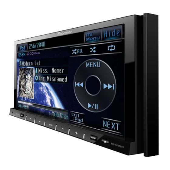
2.3 PANEL FACILITIES AVH-P4100DVD/XN/UC, AVH-P4100DVD/XNEW5 Head unit For details concerning operations, see the re- mote control manual. RESET button Press to return to the factory settings (initial settings). DISP OFF button Press to turn the information display on or off. -
Page 14: Head Unit
AVH-P4100DVD/XNUW5 Head unit Optional remote control The remote control CD-R55 is sold separately. RESET button For details concerning operations, see the re- Press to return to the factory settings (initial mote control manual. settings). DISP OFFAV/NAVI button Press to turn the information display on or off. -
Page 15: Connection Diagram
2.4 CONNECTION DIAGRAM AVH-P4100DVD/XN/UC... - Page 16 AVH-P4100DVD/XN/UC...
- Page 17 AVH-P4100DVD/XN/UC...
- Page 18 AVH-P4100DVD/XN/UC...
- Page 19 AVH-P4100DVD/XN/UC...
- Page 20 AVH-P4100DVD/XN/UC...
-
Page 21: Basic Items For Service
3. BASIC ITEMS FOR SERVICE 3.1 CHECK POINTS AFTER SERVICING To keep the product quality after servicing, please confirm following check points. Procedures Check points Confirm whether the customer complain has The customer complain must not be been solved. reappeared. If the customer complain occurs with the Display, video, audio and operations must be specific media, use it for the operation check. -
Page 22: Pcb Locations
3.2 PCB LOCATIONS IF PCB Keyboard Unit Service PCB Assy Mother PCB Monitor Unit DVD Core Unit Connect PCB Unit Number CWN3797(UC,EW5) Mother Unit Unit Number CWN3796(UW5) Consists of Unit Name Monitor Unit Mother PCB Unit Number YWX5007 IF PCB Unit Name DVD Core Unit Unit Number... -
Page 23: Jigs List
3.3 JIGS LIST DVD Module GGD1524 Mother PCB Drive Unit GGD1170 GGF1461 GGF1495 GGD1380 Monitor Unit - Jigs List Name Jig No. Remarks 60-Pin Relay PCB GGF1495 LCD <--> 60-Pin FFC (GGD1380) 60-Pin FFC GGD1380 60-Pin Relay PCB (GGF1495) <--> Monitor PCB (CN6001) 40-Pin + 20-Pin Relay PCB GGF1461 Monitor Unit (CN5001) <-->... -
Page 24: Cleaning
3.4 CLEANING Before shipping out the product, be sure to clean the following portions by using the prescribed cleaning tools: Portions to be cleaned Cleaning tools DVD pickup lenses Cleaning liquid : GEM1004 Cleaning paper : GED-008 AVH-P4100DVD/XN/UC... - Page 25 AVH-P4100DVD/XN/UC...
-
Page 26: Block Diagram
4. BLOCK DIAGRAM 4.1 OVERALL CONNECTION DIAGRAM 14 REM 13 GNDKEY 12 HDRST 11 LEDB1 10 LEDG1 9 LEDR1 8 LEDB2 7 LEDG2 KEYBOARD 6 LEDR2 MONITOR UNIT 5 KDT0 UNIT 4 KDT1 3 ILMB 2 SWVDD33 1 GNDKEY MONITOR UNIT(uCOM) MONITOR UNIT(MONITOR) CN5001 CN501... - Page 27 LCD MODULE CWX3691 CN6001 ADVY ADVY ADVX ADVX PLXV PLXV PLYV PLYV TH_G CN5001 CN501 JA402 FM/AM ANT JA141 P.B. MUTE B.REM BGSENS B.UP JA101 JA102 CN522 JA951 VCR IN RCA OUT JA2004 IP BUS AVH-P4100DVD/XN/UC...
-
Page 28: Block Diagram
4.2 BLOCK DIAGRAM MOTHER PCB (1/2) CN901 VDD5 SPDIFSENS Q951 SPDIFOUT IECOUT IC951 TC7SET08FUS1 LS_L LOUT IN1_L IPOD CP IC BUSL+ IC561 IN4+_L Q902 Q901 341S2162 BUSL- SYS+B IN4-_L CPRST nRESET LOUT IN2_L I2C_SDA/ TUN_L SPI_SOMI IN5+_L I2C_SCL/ TO 2/2 SPI_SIMO CN1901 STANBY... - Page 29 RXIE CN501 WIREDAD HDRST WIRED MFLPW MFLPWR TO 2/2 M_SRX RXMON S_MTX TXMON MONRST MONIRST ILMB :AVH-P4100DVD/XN/UC SWVDD33 ACC33 :AVH-P4100DVD/XNEW5 TO 2/2 CN5001 PWRVI :AVH-P4100DVD/XNUW5 PWVI RGBON TXNAVI PWRFL PWFL RXNAVI MONVBS RGB VIDEO ISOLATOR IC771 NJM2138V NAVI_R C_+IN C_OUT...
- Page 30 BZ601 BEEP BUZZER PWFL XOUT Q1022 P1022 X601 PWFL 15MHz MFLPW TO 1/2 Q1021 CN801 OPENSW NC(OPENSW) MOT0 MOT0 MOT1 MOT1 PULSE0 PULSE0 PULSE1 DRIVE UNIT PULSE1 INTERFACE HALFSW HALFSW HOMESW HOMESW MOTV MOT5V :AVH-P4100DVD/XN/UC :AVH-P4100DVD/XNEW5 :AVH-P4100DVD/XNUW5 TO 1/2 AVH-P4100DVD/XN/UC...
- Page 31 AVH-P4100DVD/XN/UC...
- Page 32 DVD CORE UNIT NRES VIDEO+AUD IC1501 MN2DS0018M NRES FLASH 16M IC1401 0-15 CWW1753 0-19 USB_ XCFS1 XCSSR IC1402 CWW1754 XCFS2 NEXCE XWR1 NEXWE NRES RESET NEXOE SDRAM IC1480 K4S641632N-LC75 0-11 0-15 DQM0 LDQM DQM0 DQM1 UDQM DQM1 XCAS NCAS XRAS NRAS XCSM NCSM...
- Page 33 CN1901 NRES XRESET VIDEO+AUDIO IC1501 AUDIO 2CH ANALOG OUT MN2DS0018MAUB IC1801 PCM1753DBQ NRES ANALOG LOUT SRCK LOUT SRCK VOUTL ADOUT ADOUT DATA LRCK LRCK LRCK SDODAC ISC_SCL SDODAC SCKDAC I2C_SDA SCKDAC LTDAC RESET CP_Reset LTDAC DACCK IFCOUT DACCK CN901 IC1951 TC7SZU04FU COMPOSIT COMPOSITE...
- Page 34 MONITOR UNIT GERDA IC5702 C.VIDEO MN103SE60PUB CN5001 Q5451 Q5452 LCD_R_[0-5] MONVBS IC5451 AINP0 NJM2505AF CSYNC LCD_G_[0-5] NAVI_R VIDEO_AD NAVI_G MONITOR uCON LCD_B_[0-5] IC5601 IC5101 AK5406XQ NAVI_B PE5669A8 GPIO_05 CSYNC SOGIN DVR[0-5] LCDCSY NAVI_R LCDDEN DVG[0-5] NAVI_G LCDHSY NAVI_B DVB[0-5] LCDVSY LCDCLK S_MTX RXD0/TSI...
- Page 35 LCD PANEL CN6001 LR[0-5] LG[0-5] LB[0-5] MODE COMDC VCOM AMP IC6151 VCOM DRIVE NJM082BV VCOM COMAC Q6001 Q6002 VCOM Q6151 LADDER NETWORK 11,13 10,12 IC6005 V[0,3,5,7,9,10] TC74VHCT04AFTS1 VCCM16V VCC15V VCC3.3V VSHD VSHA VCC53V PWRFL IC6101 CN6101 TK11840L Q6102 Q6103 BLSYNC 1,2,5,6 D1-4 Q6101...
-
Page 36: Diagnosis
5. DIAGNOSIS 5.1 OPERATIONAL FLOWCHART RESET Vdd : pin 23 Vdd = 3.3 V? BSENS : pin8 BSENS = L? ASENS : pin9 ASENS = L? STANDBY : pin27 STANDBY = H? ASENBO : pin123 ASENBO <- H Standby VDCNT5 : pin25 VDCNT5,8 <- H VDCNT8 : pin26 Starts... -
Page 37: Inspection Method Of Pickup Unit
5.2 INSPECTION METHOD OF PICKUP UNIT Disc to be used CD-DA: TCD-782 DVD-Video: TDV-582 Execution method Replace the PICK UP START SKEW ADJ. LD turned on? Check parts Check point: Check point: RF level check LD current check AS MAX check LD current check Is it OK? Is it OK? - Page 38 LD current check Check Status: [Foucs closed] of TEST MODE Disc Check Point Threshold Remarks: LD current GGV1025 DVDLD1-VCC5_3 60 - 390 (mV) 10 - 65 (mA) Expansion NO. Disc Check Point Threshold Remarks: LD current TCD-782 CDLD1-VCC5_3 60 - 360 (mV) 10 - 60 (mA) Expansion Notes: Please pay attention to the laser diode damage by static electricity.
- Page 39 ASMAX check ASMAX value shows the value of RF level. Status: [Foucs closed] of TEST MODE Disc Check Point Threshold Remarks: 8 digits value of Only four last digits are more than GGV1025 ASMAX displayed according to on display 0000 0B00 the product.
-
Page 40: Diagnosis Flowchart
5.3 DIAGNOSIS FLOWCHART AVH-P4100DVD/XN/UC... - Page 41 Check 1: Standby OK? <Check> Check the voltage at the “STANBY” test point while the power is on. Use the “DGND1” test point at the reference. Specification value Check point Module No. Unit VCC33 V- STANBY-DGND1 0.6 V or more Side A STANBY Fig 1.1: STANBY check point...
- Page 42 Check 2: Is VDD5 (VCC33, VCC12) power supply voltage OK? IC1401 FLASH power supply (Data) IC1402 FLASH power supply (Program) VCC33 (= 3.3 V) IC1004 IC1481 SDRAM power supply 3.3 V output regulator IC1501 DV5U power supply IC1005 VCC12 (= 1.2 V) IC1501 DV5U power supply DC/DC converter 1.2 V output...
- Page 43 Check 3: Reset OK? <Check> Check the voltage at the “XRES” test point while the power is on. Use the “DGND1” test point at the reference. Check point Module No. Specification value Unit VCC33 × 1 XRES-DGND1 0.7 or more Side A DGND1 NRES...
- Page 44 Check 4: Is VSENS OK? CN1901 HOST I/F IC1501 R1004, DV5U R1007 IC1004 Regulator IC1005 VCC12 DC/DC converter STANBY XRES Fig 4.1: Power supply configuration and VSENS <Check> Check the voltage at the “VSENS” test point while the power is on. Use the “DGND1”...
- Page 45 Check 5: 27 MHz Normal? <Outline> Each clock is created inside the IC1501 using the 27 MHz master crystal oscillator (X1501). IC1501 DVD-LSI OSCO X1501 27 MHz OSCI crystal VCC33 VCC12 Fig 5.1: Clock configuration <Check method> Turn the power on, and check with DGND being the reference. In case of NG, check the applicable line, periphery of IC1501, soldering of the peripheral components and defective components.
- Page 46 Check 6: Is SDRAM I/F OK? <Outline> In order to secure the MPEG stream data as the buffer, the capacity of communication I/F SDRAM between the LSI and the memory is 64Mbit. Be careful as XCSM, XWE, XCAS and XRAS of IC1480 are called differently in IC1501, namely NCSM, NWE, NCAS, NRAS.
- Page 47 <Check> Check the conductivity at “check point 1” and “check point 2” without power. In case of NG, check the soldering and defective components throughout the “output t input” of the applicable section. Signal name Check point 1 Check point 2 Specification value IC1480 23pin...
- Page 48 Side B Check point 1 (IC1480) Side A Check point 2 (IC1501) Fig 6.2: SDRAM I/F check point AVH-P4100DVD/XN/UC...
- Page 49 Check 7: Is VD8, VCC5 power supply voltage OK? VD8_1 F.E. driver system IC1002 VCC5 (= 5.0 V) VD8_2 Power supply REG IC for PU for VCC 5 V. Fig 7.1: Power supply configuration <Check> Check the voltage at the “VD8_1, VD and VCC5_1” test point while the power is on. Use the “PGND3 and AGND1”...
- Page 50 Check 8: Is AVCC5 voltage OK? IC1003 AVCC5 (= 5.0 V) IC1801 REG IC Audio-DAC for AVCC 5 V. Fig 8.1: Power supply configuration <Check> Playback DVD-REF-A1 TITLE 1 and check the voltage at the stylus. Check with PGND and GNDAU being the reference. Check point Module No.
- Page 51 Check 9: Is DACCLK normal? <Outline> DACCLK for Audio-DAC is created by IC1501 using the 27 MHz master crystal oscillator (X1501). IC1501 X1501 DVD-LSI IC1801 Audio-DAC DACCLK 27 MHz crystal VCC33 VCC12 Fig 9.1: Clock configuration <Check method> DVD: DVD-REF-A1 TITLE 1 CD: Playback a normal CDDA.
- Page 52 Side B Check point 1 (DACCK stylus) Side A Check point 2 (IC1501 148 pin) DGND2 Fig 9.3: 27 MHz, DACCLK check point AVH-P4100DVD/XN/UC...
- Page 53 Check 10: Is the audio circuit OK? <Outline> The serial 3 lines digital output + DACCLK, output from DVD-LSI (IC1501), are converted to analog audio signal at Audio-DAC (IC1801) and are output from the HOST I/F (CN1901). Simultaneously, the analog MUTE signal is also output from DVD-LSI (IC1501) via the HOST I/F. The digital audio signal (IECOUT), output from DVD-LSI (IC1501).
- Page 54 Side A DGND2 ADOUT LRCK Side B SRCK Fig 10.3: Serial 3 lines check points AVH-P4100DVD/XN/UC...
- Page 55 The following checks shall be conducted using the following measurement circuits with GNDAU1 being the reference. 47 kohm 47 kohm GNDAU1 Check point 1 (stylus) Specification value (rms) Reference waveform 1 400 ± 150 mV Waveform 4 1 400 ± 150 mV Waveform 4 Specification value is the root-mean-square value (rms).
- Page 56 Side A IEC DGND2 Fig 10.6: Digital audio signal (IECOUT) check point AVH-P4100DVD/XN/UC...
- Page 57 Check 11: Is the video circuit OK? <Outline> Composite signal and component signal are output from DVD-LSI (IC1501), and are output from the HOST I/F (CN1901) via a buffer circuit. CN1901 HOST I/F IC1501 DVD_LSI Composite COMPOSITE Video section Fig 11.1: Video circuit <Checking method>...
- Page 58 Side A COMPOSITE GNDV Fig 11.3: VIDEO signal check point AVH-P4100DVD/XN/UC...
- Page 59 Check 12:How to judge whether the flash memory has reached its life or not. If the reaction to user operation is slow or operation is slow in general, there is a possibility that the flash memory has reached its life. Make judgment regarding the flash memory life by looking at the display of the LD energizing time.
- Page 60 Check 13: 48 MHz Normal? <Outline> Each clock is created inside the IC1501 using the 48 MHz master crystal oscillator (X1501). IC1501 DVD-LSI X1950 48 MHz crystal USB_CLOCK VCC33 VCC12 Fig 13.1: Clock configuration <Check method> Turn the power on, and check with DGND1 being the reference. In case of NG, check the applicable line, periphery of IC1501, soldering of the peripheral components and defective components.
- Page 61 Side A IC1501 50pin DGND1 Fig 13.3: 48 MHz check point AVH-P4100DVD/XN/UC...
- Page 62 1.USB Memory: Play a song from USB memory and check D+ and D- with the DGND standards. 2.iPod: Connect iPod and check CP_RESET, SDA and SCL with the DGND standards until the pioneer log appears. Play a song from iPod and check D+/D- with the DGND standards.
- Page 63 Side A SDATA CP_ RESET SCLOCK DGND2 AVH-P4100DVD/XN/UC...
- Page 64 AUDIO CH1:LO CH2:RO CH1:ADOUT3 Reference voltage: DGND2 1 V/div. 5 usec/div Reference voltage: GNDAU2 1 V/div. 500 usec/div G-> -> -> Waveform 1 Waveform 4 CH1:SRCK CH1:IECOUT Reference voltage: DGND2 1 V/div. 5 usec/div Reference voltage: DGND2 1 V/div. 500 nsec/div G->...
- Page 65 VIDEO [WHITE 100IRE] CH1:COMPO Reference voltage: GNDV1 200 mV/div. 10 usec/div Waveform 6 USB memory USB memory USB memory Reference voltage:DGND 1 ms/div 2 V/div Reference voltage:DGND 200 ns/div 2 V/div Waveform 7 Waveform 8 AVH-P4100DVD/XN/UC...
- Page 66 iPod iPod iPod Reference voltage:DGND 1 ms/div 2 V/div Reference voltage:DGND 200 ns/div 2 V/div Waveform 9 Waveform 10 iPod iPod Reference voltage:DGND 2 ms/div 1 V/div Reference voltage:DGND 20 ms/div 1 V/div CP_RESET DGND NRES Waveform 11 Waveform 12 iPod Reference voltage:DGND 500 us/div 1 V/div Waveform 13...
-
Page 67: Error Code List
5.4 ERROR CODE LIST Generation source Method of reset UART Source Eject Play Key Error status OSD *1 Meaning Disc (MSC) (iPod) Off/On Off/On A disc containing the unplayable NON-PLAYABLE DISC Format only USB device that doesn't correspond INCOMPATIBLE DEVICE USB device of format alone that UNPLAYABLE FILE cannot be reproduced... - Page 68 X: Cancel the error by operation. -: Error is not cancelled by operation. *: No setting *1 A content displayed on OSD. As for the items having multiple display patterns, the upper row is for the Japanese version Full GUI, and the lower row is for the Touch Panel model and Full GUI (English version).
- Page 69 AVH-P4100DVD/XN/UC...
-
Page 70: Connector Function Description
5.5 CONNECTOR FUNCTION DESCRIPTION WIRED REMOTE VIDEO REAR REAR INPUT/OUTPUT CAMERA IN CONTROL OUTPUT AUX IN OPTICAL OUTPUT ANTENNA AUDIO SUBWOOFER INPUT OUTPUT IP-BUS INPUT FRONT 3 5 7 9 11 13 15 OUTPUT 4 6 8 10 12 14 16 RGB INPUT(UW5) 1. -
Page 71: Service Mode
6. SERVICE MODE 6.1 MONITOR TEST MODE [Method for Mode IN] When the reset start is done while pushing MUTE and TRACK DOWN, it shifts to the monitor test mode. [Display specifications] [Operation specification] Operational description Remote controller key Selection cursor up movement Selection cursor down movement Menu enter 1. - Page 72 2. Touch Panel Calibration [How to activate the touch panel test mode] Choose "Touch Panel Calibration" among the monitor test mode menu screen. [Menu types in the mode] The calibration test mode consists of the following menus. Top menu Outermost circumference inspection 16 points adjustment Coordinate inspection Calibration verification...
- Page 73 [Outermost circumference inspection] [Outline] Outermost circumference value of X and Y is obtained by tracing the outermost circumference of the touch panel screen. When exiting the menu screen by pressing 5 key, the captured value is stored in the EEPROM. Furthermore, when storing the value, checking is made as to whether the value is within the range or not.
- Page 74 [16 points adjustment] [Outline] When correctly touched, the cursor will disappear, and the next cursor will appear. Calibration is conducted by repeating this process 16 times. When the 17th point has been finally touched, setting information for the 16 points and the normal ending information, total of 17 byte data, are written into the EEPROM, and the screen returns to the TOP menu.
- Page 75 [Coordinate inspection] [Outline] The coordinate before correction and after correction at the time of pressing the touch panel are displayed for coordinate verification. Furthermore, the red "+" cursor can be moved by the key operaiont mentioned bellow, and the coordinate of the cursor center is displayed.
- Page 76 [Calibration verification] [Outline] Touch the cursor “+” displayed on the screen. The correct touch will delete the cursor and another cursor will be displayed. The incorrect touch will make the characters of cursor turn red. Repeat this for 4 points, and “OK” is displayed upon the last press of 4th point. [Display specifications] confirming The pushing order...
- Page 77 [Data initialization] [Outline] Result of outermost circumference inspection and of calibration inspection (corrected value) are returned to their initial values. As for the initialized items, the initial values are written into the EEPROM and the adjustment information is cleared. [Display specifications] Conditions for the adjustment completion mark (*) to be lighted up.
- Page 78 3. EEPROM Adjust [Method for Mode IN] Choose "EEPROM Adjust" among the monitor test mode menu screen. [Display specifications] Flicker Adjust Backlight output max value : 196 Backlight output min value : 83 Dimmer threshold value (high) : 192 Dimmer threshold value (low) : 96 Dimmer external light point (high) : 255 Dimmer external light point (medium) : 135 Dimmer external light point (low) : 0...
- Page 79 LCD protection value at High temperature (1) Temperature value : 0 LCD protection value at High temperature (1) Dimmer output : 0 LCD protection value at High temperature (1) Target arrival time : 6 LCD protection value at High temperature (2) Temperature value : 0 LCD protection value at High temperature (2) Dimmer output : 4...
- Page 80 Common inverted output amplitude adjusted value : 173 Brightness adjustment : 32 Noise shaping setting : 1 RGB gamma correction : 0 RGB gamma correction setting R polygonal line position setting arrangement [3] : 31 RGB gamma correction setting R polygonal line position setting arrangement [4] : 39 RGB gamma correction setting R polygonal line position setting arrangement [5] : 47 RGB gamma correction setting...
- Page 81 RGB gamma correction setting R gain arrangement [3] : 32 RGB gamma correction setting R gain arrangement [4] : 32 RGB gamma correction setting R gain arrangement [5] : 32 RGB gamma correction setting R gain arrangement [6] : 32 RGB gamma correction setting G gain arrangement [3] : 32 RGB gamma correction setting...
- Page 82 R cutoff adjustment +3 : 64 G cutoff adjustment +3 : 64 R cutoff adjustment +2 : 64 G cutoff adjustment +2 : 64 R cutoff adjustment +1 : 64 G cutoff adjustment +1 : 64 B cutoff adjustment -1 : 64 G cutoff adjustment -1 : 64 B cutoff adjustment -2 : 64 G cutoff adjustment -2 : 64...
- Page 83 Synchronous separation Top curl adjustment (Strong electric field, TV) Dcs1_ilgain1 Synchronous separation Top curl adjustment (Strong electric field, TV) Dmv1_ilgain1 Synchronous separation Top curl adjustment (Strong electric field, TV) Dcs1_ilgain23 : 56 Synchronous separation Top curl adjustment (Strong electric field, TV) Dmv1_ilgain23 : 56 Synchronous separation...
- Page 84 Synchronous separation Top curl adjustment (Super-weak electric field, TV) Dcs25_ilgain1 : 39 Synchronous separation Top curl adjustment (Super-weak electric field, TV) Dmv25_ilgain1 Synchronous separation Top curl adjustment (Super-weak electric field, TV) Dcs25_ilgain23 : 39 Synchronous separation Top curl adjustment (Super-weak electric field, TV) Dmv25_ilgain23 : 39 Synchronous separation...
- Page 85 Synchronous separation Top curl adjustment (Non signal, TV) Dycomp5_ilgain1 Synchronous separation Top curl adjustment (Non signal, TV) Dycomp5_ilgain23 : 39 Synchronous separation Top curl adjustment (Non signal, Besides TV) Dycomp5_ilgain1 Synchronous separation Top curl adjustment (Non signal, Besides TV) Dycomp5_ilg : 39 Electric field strength judgment value for TV Dwec_th_cs225 : 150 Electric field...
- Page 86 Color demodulate part UV delay adjustment (ulNT358_AVICOL3_03) : 27 Color demodulate part UV delay adjustment (ulPALBG_AVICOL3_03) : 27 Color demodulate part UV delay adjustment (ulPALM_AVICOL3_03) : 26 Color demodulate part UV delay adjustment (ulPALN_AVICOL3_03) : 26 Color demodulate part UV delay adjustment (ulSECAM_AVICOL3_03) : 26 Color demodulate part Phase killer value (ulNT358_AVICOL1_09) : 2 Color demodulate part...
- Page 87 4. EEPROM Initialize [Method for Mode IN] Choose "EEPROM Initialize" among the monitor test mode menu screen. [Display specifications] Default of a cursor is the location of "No". Choose "YES" and decide, initialize a setting value. *) Don't turn off power while initializing. When normally ends, "success"...
- Page 88 5. Display Test (Test Pattern) [Method for Mode IN] Choose "Display Test (Test Pattern)" among the monitor test mode menu screen. [Display specifications] [Operation specification] Operational description Remote controller key Selection cursor up movement Selection cursor down movement Selection cursor left movement Selection cursor right movement Return to test mode mene Menu enter...
- Page 89 [FLICKER ADJUSTER] Display of monochrome stripe signal of the flicker adjustment [Operation specification] Operational description Remote controller key Return to test mode mene [RAMP & 10STEP] Display of step signal and signal for alpha blend check [Operation specification] Operational description Remote controller key alpha blend rate up alpha blend rate down...
- Page 90 [RASTER SIGNAL] Display of signal for step confirmation [Operation specification] Operational description Remote controller key Return to test mode mene Next signal [CONTRAST] Display of Black/White signal [Operation specification] Operational description Remote controller key Return to test mode mene Next signal [CENTER MARKER] Display of signal for screen central location setting.
-
Page 91: Dvd Test Mode
6.2 DVD TEST MODE Test mode display will not appear on the display of this product. Connect the rear monitor output to a monitor. Image of the test mode. [VOL-] + [TRACK UP] + Reset start Switch position of the remote control unit. [AVH mode] (1)-(8) and EJECT is the key of remote control unit. - Page 92 2 x 00 0000 (3),(4) Focus Jump CRG +/- Power_OFF Tracking balance When L0 layer: 2000 0000 It operates while the key 2FFF 0000 When L1 layer: 2100 0000 is being pressed. 2B00 0000 : CRG+ TBAL coefficient (layer 0) 2C00 0000 : CRG- TBAL coefficient (layer 1) TE normalization coefficient (layer 0)
- Page 93 Legend: … Key operation EDC. Image of the test mode … Operational state … The content displayed on the DVD mechanism (video only) 8 characters data is sent to the product side (HOST) by UART communication. EDC1/2 test mode [Note] Image is the same for both EDC1 and EDC2. 0000 0000 EJECT operation [Note] Eject can be effected any time during the EDC test mode.
- Page 94 Simple test mode The selection of the figure of each screen can be selected by "Key command for the test". <Flow chart> TEST MODE 1: LD ON 2: ASMAX 3: Skew Adjustment 4: Error Rate 5: CRG Move Outer 6: Eject Please Input Number 1 select 1: DVD Single Layer...
-
Page 95: Dvd Touch Panel Test Mode
6.3 DVD TOUCH PANEL TEST MODE How to enter: Reset with [VOL-] key and [TrackDOWN] key pressed. How to unlock: Product reset Turning ACC ON Summary: It is for temporary analysis in services. (For temporary analysis of user claim and etc. against DVD touch direct.) (1)Display a frame border in the valid area as a button in the contents by OSD of DVD mecha on DVD-Video menu time. -
Page 96: Disassembly
7. DISASSEMBLY Removing the Panel and Holder (not shown) (EW5, UW5) 1. Remove the Panel. 2. Remove the eight screws and then remove the Holder. 3. Remove the four screws and then remove the Left and Right Holder. Removing the Monitor Assy (Fig.1, 2, 3) Remove the two screws.(Fig.1) Fig.1 Monitor Assy... - Page 97 Removing the Keybord Unit (Fig.7, 8) Remove the three hooks and then remove the Keybord Unit.(Fig.7) Fig.7 Attention when the Keyboard Unit are exchanged.(Fig.8) Keybord Unit _ Refer to figure for how to bend the Cable. _ Notes after exchanges. Fig.8 The following items after the Keyboard Unit •...
- Page 98 Removing the DVD Mechanism Module (Fig.13) Remove the four screws. Disconnect the cable and then remove the DVD Mechanism Module. Fig.13 DVD Mechanism Module Removing the Chassis(Upper) (Fig.14, 15) Holder Remove the two screws. (Fig.14) Remove the five screws and then remove the Heat Sink. (Fig.14) Heat Sink Remove the Holder.
- Page 99 Removing the Mother Unit (Fig.16) Mother Unit Disconnect the cable. Remove the screw. Remove the four screws and then remove the Mother Unit. Fig.16 NOTE: When you remove the top case Don't put tweezers or something into these holes to remove the top Use these holes to remove the top case case.
- Page 100 How to have it 1.Have a specified part. Handling OK Handling NG AVH-P4100DVD/XN/UC...
- Page 101 Mecha Module_Bringing into the Clamp State with No Disc Loaded 1. Remove the relay FFC from the connector on the module PCB side (Fig. 1). (Precaution) When it is difficult to apply 4V to the motor in procedure 2 below, remove the connector on the relay PCB side, then remove the FFC, and remove the solder of the CRG motor lead and apply voltage to the lead.
- Page 102 CRG Mecha_Bringing into the Clamp State with No Disc Loaded 1.Remove the T-case washer and then remove the drive gear. (Fig. 1) 2.Lift the clamp arm assy until it is in the state shown in Fig. 2_b (open-lock state). 3.Put your finger on the area A of Fig. 2_c and then slide it to the direction of the arrow (the direction of the playing state). 4.Push down the clamp arm.
- Page 103 Removing the Module PCB 1.Short-circuit two spots on the land of the pick up FPC. (Fig. 1) 2.Remove the pick up FPC and the relay FFC from the connector. (Fig. 2) 3.Temporarily attach the pick up FPC to the pick up rack. (Fig. 3) (in order to prevent the damage to the pick up FPC) 4.Remove the two PCB clinch screws and then remove the module PCB.
- Page 104 Removing the PU Unit 1.Hook the feed screw biasing spring on the temporary hook (Fig. 2b). Be careful not to get injured by the tip of the spring. 2.Hold the PU at the location A in Fig. 1 and slide and scoot it to the direction of the inner periphery. 3.As in Fig.
-
Page 105: Each Setting And Adjustment
8. EACH SETTING AND ADJUSTMENT 8.1 DVD ADJUSTMENT 1) Precautions This product uses 5 V and 3.3 V as standard voltages. If the reference voltage is connected to GND by The electrical potential that is the reference for signals, mistake, turn the regulator OFF immediately, or is not GND, but VREF (approximately 2.2 V) and VHALF turn the power OFF. - Page 106 - SKEW adjustment When one of the following replacements has taken place, SKEW adjustment for the pick up will be required. (1) Replacement of the pick up unit (2) Replacement of the spindle motor (3) Replacement of the carriage chassis (4) Replacement of the main shaft of the pick up unit Measurement equipment and tools/jigs: Oscilloscope Driver for SKEW adjustment ->...
- Page 107 There are two methods of making adjustment: a method of making adjustment through monitoring RF waves by the oscilloscope (method 1) and a method of making adjustment through checking the numerical value of the RF level by OSD (method 2). Adjusting procedure is shown below, but regarding how to start the test mode and the operating procedure, please refer to the clause on the service test mode.
- Page 108 Skew Adjustment 1: Power OFF RF Level : 000000 Please Input Number 9. Skew Adjustment Select “1: Power OFF.” Skew Adjustment 1: Power OFF RF Level : 000000 Please Input Number 10. TEST MODE Select “6: Eject.” TEST MODE 1: LD ON 2: ASMAX 3: Skew Adjustment 4: Error Rate...
- Page 109 Disc Detection Arm 13. CRG Move Outer Select “1: DVD Single Layer.” CRG Move Outer 1: DVD Single Layer 2: DVD Dual Layer 3: CD 4: CD-RW 5: Return Please Input Number The pickup moves to the outer periphery. Apply the adhesive to fix the skew, the resonance adhesive and the screw lock. Refer to the next page regarding the locations of adhesive joining.
- Page 110 Locations to make SKEW adjustment Locations to adhere the SKEW 1,2,3: BOND QUICK MENDER AVH-P4100DVD/XN/UC...
- Page 111 Bond for resonance 4:Three Bond 1530 adhesive Bond for locking the screw 5,6 : Three Bond 1401M Bond for locking the screw AVH-P4100DVD/XN/UC...
- Page 112 Precautions on handling the PU *Precaution: Do not touch those shaded areas in the following figures. Hologram (Beware of the static) Do not touch the optical part RF level adjusting part Do not touch the spring AVH-P4100DVD/XN/UC...
-
Page 113: Monitor Unit Adjustment
8.2 MONITOR UNIT ADJUSTMENT MONITOR UNIT(SIDE B) - Adjustment Point VCC33 PWRVI -16V MONVBS COMDC AVH-P4100DVD/XN/UC... - Page 114 AVH-P4100DVD/XN/UC...
- Page 115 AVH-P4100DVD/XN/UC...
-
Page 116: Pcl Output Confirmation
8.3 PCL OUTPUT CONFIRMATION - PCL output In the normal operation mode (with the detachable panel installed, the ACC switched ON, the standby mode cancelled), shift the TESTIN IC601(Pin 87) terminal to H. The clock signal is output from the CLKOUT terminal IC601(Pin 62). The frequency of the clock signal is 625 000 Hz that is one 32th of the fundamental frequency. -
Page 117: Exploded Views And Parts List
9. EXPLODED VIEWS AND PARTS LIST OTES : Parts marked by " * " are generally unavailable because they are not in our Master Spare Parts List. The > mark found on some component parts indicates the importance of the safety factor of the part. Therefore, when replacing, be sure to use parts of identical designation. -
Page 118: Packing(Avh-P4100Dvd/Xn/Uc)
9.1 PACKING(AVH-P4100DVD/XN/UC) AVH-P4100DVD/XN/UC AVH-P4100DVD/XN/UC... - Page 119 PACKING(AVH-P4100DVD/XN/UC) SECTION PARTS LIST Mark No. Description Part No. Mark No. Description Part No. 12-1 Owner's Manual CRB2897 Cord Assy CDP1219 12-2 Owner's Manual CRB2898 Cord Assy CDP1166 12-3 Owner's Manual CRB2983 Screw Assy CEA2788 12-4 Installation Manual CRD4377 Polyethylene Bag CEG-127 Screw BMZ50P080FTC...
-
Page 120: Packing(Avh-P4100Dvd/Xnew5, Xnuw5)
9.2 PACKING(AVH-P4100DVD/XNEW5, XNUW5) AVH-P4100DVD/XNEW5 AVH-P4100DVD/XNUW5 AVH-P4100DVD/XN/UC... - Page 121 See Contrast table(2) Polyethylene Bag CEG1426 Contain Box See Contrast table(2) Sheet CNN3089 Protector CHP3708 CNV8969 (2) CONTRAST TABLE AVH-P4100DVD/XNEW5 and AVH-P4100DVD/XNUW5 are constructed the same except for the following: Mark Description AVH-P4100DVD/XNEW5 AVH-P4100DVD/XNUW5 Unit Box CHG6728 CHG6729 Contain Box CHL6728 CHL6729...
-
Page 122: Exterior(1)
9.3 EXTERIOR(1) AVH-P4100DVD/XN/UC... - Page 123 See Contrast table(2) Pin Jack(JA2003) CKB1065 Sheet See Contrast table(2) Pin Jack(JA102) CKB1085 Plug(JA141) CKM1376 (2) CONTRAST TABLE AVH-P4100DVD/XN/UC, AVH-P4100DVD/XNEW5 and AVH-P4100DVD/XNUW5 are constructed the same except for the following: Mark Description AVH-P4100DVD/XN/UC AVH-P4100DVD/XNEW5 AVH-P4100DVD/XNUW5 Screw Not used BMZ30P060FTC BMZ30P060FTC...
-
Page 124: Exterior(2)
9.4 EXTERIOR(2) EW5, UW5 AVH-P4100DVD/XN/UC... - Page 125 See Contrast table(2) Holder CND4805 Holder CND4807 Keyboard Unit See Contrast table(2) Insulator CNN2596 Insulator CNN2778 (2) CONTRAST TABLE AVH-P4100DVD/XN/UC, AVH-P4100DVD/XNEW5 and AVH-P4100DVD/XNUW5 are constructed the same except for the following: Mark Description AVH-P4100DVD/XN/UC AVH-P4100DVD/XNEW5 AVH-P4100DVD/XNUW5 Grille CNS9812 CNS9812 CNS9665 Monitor Unit...
-
Page 126: Exterior(3)
9.5 EXTERIOR(3) Spreads it on the entire gear GEM1024 GEM1043 GEM1048 AVH-P4100DVD/XN/UC... - Page 127 EXTERIOR(3) SECTION PARTS LIST Mark No. Description Part No. Drive Unit CXE1173 Screw AMZ26P030FTC Screw BMZ26P030FTC Screw(M2 x 2) CBA2129 Washer CBF1039 Screw EBA1049 Spring EBH1684 Spring EBL1031 Spring EBL1032 Slit board ENC1582 Bracket ENC1586 Insulator ENM1048 Spacer ENM1049 Insulator ENM1051 Arm(White) ENV1615...
-
Page 128: Dvd Mechanism Module
9.6 DVD MECHANISM MODULE ( C ) ( C ) ( C ) ( B ) ( A ) ( A ) ( C ) ( A ) ( A ) ( C ) ( A ) ( C ) ( C ) ( C ) ( C ) - Page 129 DVD MECHANISM MODULE SECTION PARTS LIST Mark No. Description Part No. Mark No. Description Part No. Holder CNW1195 Screw BMZ20P020FTC Screw BSZ20P040FTC Damper CNW1197 Screw(M2 x 4) CBA1835 Damper CNW1198 Washer CBF1038 Connect PCB Unit CWX3618 Spring CBH2860 Connector(CN701) CKS6003 Connector(CN101) CKS6063 Spring...
- Page 130 ( A ) ( A ) ( C ) ( C ) ( C ) ( C ) ( C ) ( C ) ( C ) ( A ) ( A ) ( A ) (A) : GEM1045 (B) : GEM1038 (C) : GEM1024 AVH-P4100DVD/XN/UC...
- Page 131 AVH-P4100DVD/XN/UC...
-
Page 132: Schematic Diagram
10. SCHEMATIC DIAGRAM 10.1 MOTHER PCB(ANALOG) Note: When ordering service parts, be sure to refer to " EXPLODED VIEWS AND PARTS LIST" or "ELECTRICAL PARTS LIST". JA102 VCR:+8.2 dBs CN2002 IP-BUS&NAVI&WIRED VCR IN CN121 C111 0.1u/50 GNDRF GNDA BUP_1 MALS068X GNDA D104 14.4V... - Page 133 NOTE : NM : No Mount Symbol indicates a resistor. FM(UC): +7.1 dBs No differentiation is made between chip resistors and AM(UC): -2.9 dBs discrete resistors. FM(EW5):+11.1 dBs AM(EW5): +1.1 dBs Symbol indicates a capacitor. RCAOUT IP-BUS:+13.3 dBs No differentiation is made between chip capacitors and R IN AUX:+13.3 dBs discrete capacitors.
-
Page 134: Mother Pcb(Tuner)
10.2 MOTHER PCB(TUNER) MOTHER PCB(TUNER) CHIP SIZE LEGEND FM/AM TUNER UNIT 1608 2125 SYS+B 3216 8.4V GNDBE TUN_R TUN_L GNDBE2 EW5,UW5 Q403 E1 1 6 C1 HSLK B1 2 5 B2 GNDBE GNDBE C2 3 FM(100%)(UC):-14.0 dBs UMH1N AM(30%)(UC):-24.0 dBs FM(100%)(EW5):-10.0 dBs RDSLK AM(30%)(EW5):-20.0 dBs... - Page 135 AVH-P4100DVD/XN/UC...
-
Page 136: Mother Pcb(System)(Guide Page)
10.3 MOTHER PCB(SYSTEM)(GUIDE PAGE) Large size SCH diagram MONITOR UNIT CN5001 CN101 Guide page CN801 CN501 13.5V PWVI 7.8V Detailed page GNDD ACC33 PWFL MOTV 3.3V GNDD GNDV GNDMP GNDFL 8.1V SYSTEM MICOM C618 1u/10 R674 TVON D605 IC602 S-80827CNNB-B8M R626 GNDD AVSDA... - Page 137 MOTHER PCB(SYSTEM) C785 10u/6.3 C779 10u/6.3 C775 10u/6.3 C786 10u/6.3 C787 10u/6.3 R788 IC771 C776 10u/6.3 C777 10u/6.3 7 B_OUT C_OUT 10u/6.3 C778 C_-IN 6 B_-IN 5 B_+IN C_+IN SYS+B A_+IN D_+IN Q771 R798 D_-IN A_-IN GNDD 2SC4081(QRS) D_OUT A_OUT R793 R786 NJM2138V...
- Page 138 AVH-P4100DVD/XN/UC...
- Page 139 AVH-P4100DVD/XN/UC...
- Page 140 AVH-P4100DVD/XN/UC...
- Page 141 AVH-P4100DVD/XN/UC...
-
Page 142: Mother Pcb(Power Supply)
10.4 MOTHER PCB(POWER SUPPLY) CHIP SIZE LEGEND 1001 VDD33V 1341 MOTV 1021 PWVI,PWFL 1381 MOT5V 1608 1401 ACC33V 1061 SYS+B 2125 1421 SWVDD33V 1081 TUN3.3V 1500 1121 HIOUT12V 3216 1201 ACC33V ACC33 IC1401 3.3V TP1401 Q1422 4.8V D1401 5.1V VOUT SWVDD (NC) RB551V-30... - Page 143 MOTHER PCB(POWER SUPPLY) POWERBUS BUP_1 SIDE_A TP1003 VDD33V VDD33 S-812C33AUA-C2N TP1001 TP1002 3.3V Q1002 S1G-6904G2P 2SD1664(PQR) D1002 2SB1132(RS) Q1001 IC1001 C1005 1000u/16 CEAT102M16-P30 PWFL GNDD PWFL 7.8V 8.1V L1022 Q1022 TP1021 P1022 R1024 CTH1262-A 2SB1132(QRS) 100uH > CEK1283-A (1.75A) PWVI PWVI R1021 R1022...
-
Page 144: If Pcb
10.5 IF PCB CHIP SIZE LEGEND 1608 2125 3216 CN2002 BUS- BUS+ ASENBO BUSR+ BUSR- BUSL+ BUSL- AUXL AUAGND AUXR MAINTEST AUVGND AUXV BCAM_IN BCAM_VGGND GNDV GNDD WIREDAD WIRED CN121 GNDSIG CN2001 GNDD GNDV R2004 TP2015 GNDSIG R2006 TP2016 R2007 TP2017 GNDSIG R2003... -
Page 145: Mini Jack
LEGEND IF PCB IP BUS JA2004 BUS+ D2002 BUS+ C2002 MALS068X BUSG 0.1u/50 BUSLG TP2029 R2019 MAINTEST D2007 BUS- BUS- BUSG MALS068X BUSRG BUSL+ BUSL+ ASENB ASENBO BUSR+ BUSR+ BUSR- IP-BUS:+2.2 dBs BUSR- BUSL- BUSL- R2013 R2014 AUX:+2.2 dBs R2020 JA2002 MINI JACK R2021... -
Page 146: Dvd Core Unit(Guide Page)
10.6 DVD CORE UNIT(GUIDE PAGE) (2125) C1801 R1803 ROUT ADAC D1901 C1806 D1902 C1808 R1601 R1955 GNDAU1 R1954 GNDV C1673 27.000MHz R1602 GNDAU CSS1768 R1804 LOUT X1501 R1673 NM R1675 X2 3 GND2 (2125) R1679 GNDD R1670 R1671 GND1 R1603 C1601 AUDIO 2CH ANALOG OUT C1674... - Page 147 DVD CORE UNIT FOCUS SERVO LINE TRACKING SERVO LINE VCC33 1000->1049 :POWER SUPPLY 1100->1199 CARRIAGE SERVO LINE 1200->1299 :ACT+SPDL R1601 1400->1449 :FLASH SPINDLE SERVO LINE AGND2 :SDRAM 1480->1499 1500->1599 :DVN(SYS) RF SIGNAL GNDA 1600->1669 :DVN(FE) 1670->1699 :DVN(BE) 1700->1749 :VIDEO R1602 1800->1849 :AUDIO (ANALOG) 1850->1899...
- Page 148 AVH-P4100DVD/XN/UC...
- Page 149 PICKUP UNIT (SERVICE) AVH-P4100DVD/XN/UC...
- Page 150 AVH-P4100DVD/XN/UC...
- Page 151 AVH-P4100DVD/XN/UC...
-
Page 152: Connect Pcb
10.7 CONNECT PCB CONNECT PCB CN701 GND_B GND3 GND2 GND1 HOME HOME1 HOME1_B HOME HOME_B S101 R101 HOME 8SNS CSN1068-A DSCSNS 8SNS HALL BIAS+ 8SNS1 8SNS1_B 8SNS0 8SNS0_B S103 R102 COIL W COIL U CSN1068-A COIL V CN1201 DSCSNS HALL W+ DSCSNS1 DSCSNS1_B DSCSNS0... - Page 153 AVH-P4100DVD/XN/UC...
-
Page 154: Keyboard Unit
10.8 KEYBOARD UNIT SWVDD33 ILMB U3001 GND2 1 R3005 OUT 2 GNDKEY RS-470 HDRST LEDB1 LEDB1 LEDG1 LEDG1 LEDR1 LEDR1 LEDB2 LEDB2 CN5003 LEDG2 LEDG2 LEDR2 LEDR2 KDT0 KDT1 ILMB ILMB SWVDD33 GNDKEY 8.0V D3005 GNDKEY NSSM038A-6430 0.1u/16 C3012 0.1u/16 C3013 0.1u/16 C3014... - Page 155 KEYBOARD UNIT SWVDD33 U3001 C3005 GND2 1 0.1u/50 OUT 2 GND1 0.0~0.5V 0.5~1.4V 1.4~2.2V 2.2~3.0V 3.0~3.3V RS-470 GNDKEY KDT0 EJECT MUTE VOL+ VOL- DISP.OFF KDT1 SOURCE FORWARD REVERSE R3010 R3008 R3009 R3006 R3007 R3011 1.8k 3.9k 1.8k 3.9k EJECT MUTE VOL+ VOL- RESET...
-
Page 156: Monitor Unit(Ucom)(Guide Page)
10.9 MONITOR UNIT(uCOM)(GUIDE PAGE) CN5101 GNDOSD L5101 CTF1635-A TO TOUCH PANEL GNDOSD CN5401 PWCTL D5402 UDZS5R6(B) TP5101 C5407 1000p/50 D5403 ADVX R5405 UDZS5R6(B) C5408 VADRES VADRES VADSDA 1000p/50 VADSDA PLXV VADSCL D5404 R5402 VADSCL GRST UDZS5R6(B) GRST R5112 TESTIN C5409 1000p/50 PLYV D5405... - Page 157 CHIP SIZE LEGEND 1608 MONITOR UNIT(uCOM) 2125 3216 3225 GD33V FLASH ROM GNDOSD CONNECTOR PART 5001 CON PART 5101 R5244 IC5201 FLASH ROM PART 5201 PEH208A8 SD RAM PART 5301 R5224 FAD_15 R5201 FAD_16 TOUCH PANEL PART 5401 FAD_14 R5202 C.VIDEO PART 5451 BYTE...
- Page 158 AVH-P4100DVD/XN/UC...
- Page 159 TO BACKLIGHT AVH-P4100DVD/XN/UC...
- Page 160 AVH-P4100DVD/XN/UC...
- Page 161 AVH-P4100DVD/XN/UC...
-
Page 162: Monitor Unit(Monitor)(Guide Page)
10.10 MONITOR UNIT(MONITOR)(GUIDE PAGE) VCC3.3V 3.3V VCC33 POWER SUPPLY MAX2.0A PWRVI +15V -16V L5506 Discharge Part CTF1488-A VCC8V Q5505 GD33V (3216) 3.3V 8.0V R5536 3.3V IMZ4 Q5561 DCG1 GD33V L5502 R5564 GNDP DCG2 R5562 R5563 CTH1249-A GNDP 6.8k PWCT2 10uH R5537 68uH R5561... - Page 163 MONITOR UNIT(MONITOR) CN5701 GD33V ge Part Q5561 DCG1 R5564 DCG2 R5563 6.8k R5565 4.7k UMX2N GNDD Q5562 IC6005 DCG3 R5569 DCG4 1A 1 14 Vcc R5568 1Y 2 13 6A 6.8k R5570 2A 3 12 6Y 4.7k 2Y 4 11 5A UMZ1N 10 5Y 9 4A...
- Page 164 TO LCD MO AVH-P4100DVD/XN/UC...
- Page 165 TO LCD MODULE AVH-P4100DVD/XN/UC...
- Page 166 AVH-P4100DVD/XN/UC...
- Page 167 AVH-P4100DVD/XN/UC...
-
Page 168: Service Pcb Assy
10.11 SERVICE PCB ASSY AVH-P4100DVD/XN/UC... - Page 169 SERVICE PCB ASSY CN801 AVH-P4100DVD/XN/UC...
-
Page 170: Waveforms
10.12 WAVEFORMS - DVD CORE UNIT Note:1. The encircled number denote measuring points in the circuit diagram. 2. Reference voltage: 1.65 V(TD1,FD1)(=VHALF) 2.2 V(RF)(=VREF) In the waveform, it is seeing on the GND standard. Offset of 1.65 V or 2.2 V is put in. RF 0.2 V/div(AC) 100 ns/div RF 0.2 V/div(AC) 50 ns/div CDRF(x4CLV) - Page 171 CH1:TD1 0.5 V/div 20 ms/div CH1:TD1 0.5 V/div 10 ms/div CH1:TD1 0.5 V/div 20 ms/div CH2:COP-COM 2.0 V/div 20 ms/div CH2:COP-COM 2.0 V/div 10 ms/div CH2:COP-COM 2.0 V/div 20 ms/div Traverse 5001REV(long)(DVD) Traverse 1001REV(short)(DVD) Traverse 5001FWD(long)(DVD) VHALF VHALF VHALF 0-> 0->...
-
Page 172: Pcb Connection Diagram
11. PCB CONNECTION DIAGRAM 11.1 MOTHER PCB NOTE FOR PCB DIAGRAMS 1.The parts mounted on this PCB include all necessary parts for several destination. For further information for respective destinations, be sure to check with the schematic dia- gram. 2.Viewpoint of PCB diagrams Capacitor Connector S/PDIF OUT... - Page 173 SIDE A VCR IN RCA OUT JA102 IC181 JA101 P130 Q183 C109 C186 R115 R119 R109 R108 Q182 R117 R113 R103 R112 R116 Q101 R102 R185 D103 R104 R186 R189 P101 R105 Q102 Q104 ANTENNA D182 D102 R120 JA402 Q121 R122 R125 Q103...
- Page 174 MOTHER PCB > P 1021 (B,137,20) Fuse 1 A CEK1280 > P 1022 (B,136,17) Fuse 1.75 A CEK1283 > P 1201 (B,19,46) Fuse 4 A CEK1344 D101 P102 Q105 C111 R181 Q181 R214 C201 R225 C218 R223 P401 IC201 C219 IC202 L401 R208...
- Page 175 SIDE B D101 C194 R181 D142 D141 Q181 C195 D183 D184 R225 C218 C219 R217 IC202 R201 R180 R203 R798 Q771 R178 Q165 D167 D1002 Q1001 D163 IC771 R786 Q162 R1001 D162 R177 C167 D1001 C1007 L163 Q164 C1006 C164 R175 D166 R169...
-
Page 176: Dvd Core Unit
11.2 DVD CORE UNIT DVD CORE UNIT SIDE A C1528 R1528 R1531 R1530 R1541 C1517 R1525 C1953 R1519 C1524 C1523 C1526 R1523 R1513 R1516 C1522 R1524 R1509 R1538 C1503 C1622 C1624 C1620 C1619 C1621 L1512 C1625 C1618 C1615 C1616 C1614 C1612 C1611 C1610... - Page 177 DVD CORE UNIT SIDE B C1950 C1486 C1485 R1489 C1407 C1493 C1408 C1480 C1490 C1301 AVH-P4100DVD/XN/UC...
-
Page 178: Connect Pcb
11.3 CONNECT PCB CONNECT PCB SIDE A CN1201 CN701 LOAD/CRG MOTOR AVH-P4100DVD/XN/UC... - Page 179 CONNECT PCB SIDE B SPINDLE MOTOR S101 HOME CN101 DSCSNS R102 S102 R101 C101 8SNS R103 S103 AVH-P4100DVD/XN/UC...
-
Page 180: Keyboard Unit
11.4 KEYBOARD UNIT KEYBOARD UNIT SIDE A C3006 R3008 C3014 C3015 R3001 C3012 AVH-P4100DVD/XN/UC... - Page 181 KEYBOARD UNIT SIDE B CN5003 AVH-P4100DVD/XN/UC...
-
Page 182: Monitor Unit
11.5 MONITOR UNIT MONITOR UNIT BACKLIGHT CN6101 C5013 R5211 R5239 R5201 R5202 R5203 R5205 R5204 R5206 R5207 R5208 R5209 R5210 R5213 R5215 R5324 R5216 IC5201 R5217 R5345 R5327 R5218 R5326 C5308 L5302 R5219 C5307 R5220 C5016 R5221 C5309 R5222 C5305 R5223 R5240 R5212... - Page 183 SIDE A C5502 C5505 C5504 C5506 C5503 C5501 R5239 L5502 L5503 L5501 R5224 C5014 R5244 R5226 R5228 L5507 R5230 C5510 R5232 R5538 R5503 Q5505 C5203 R5536 C5509 IC5201 R5519 Q5502 C5539 R5245 R5537 D5502 R5234 R5515 C5543 R5236 C5528 Q5501 R5238 C5560 R5520...
- Page 184 MONITOR UNIT VCC33 PWRVI L5506 C5555 L5510 R5533 R5525 C5524 R5528 R5869 C5756 R5504 C5547 C5545 C5533 R5532 R5513 R5506 D5504 C5757 C5544 R5530 R5510 C5532 C5754 C5536 C5755 R5511 C5511 C5535 L5508 R5858 R5860 C5516 C5552 D5503 R5856 R5854 R5505 C5514 C5538...
- Page 185 SIDE B R5898 R5896 R5869 C5756 C5757 C5754 C5755 R5861 R5859 C5750 C5751 R5855 R5853 R5852 R5847 R5844 R5842 5843 R5838 C5744 C5745 R5832 R5830 R5828 R5825 R5827 R5823 C5743 C5742 IC5702 R5821 R5817 R5815 C5739 C5736 R5819 R5808 R5812 R5810 R5806 R5798...
-
Page 186: Service Pcb Assy
11.6 SERVICE PCB ASSY SERVICE PCB ASSY SIDE A CN801 AVH-P4100DVD/XN/UC... - Page 187 SERVICE PCB ASSY SIDE B AVH-P4100DVD/XN/UC...
-
Page 188: If Pcb
11.7 IF PCB SIDE B SIDE A IF PCB IF PCB D2011 R2021 R2020 R2013 R2014 D2003 C2004 R2002 R2010 R2005 R2009 AVH-P4100DVD/XN/UC... -
Page 189: Electrical Parts List
12. ELECTRICAL PARTS LIST NOTE: Parts whose parts numbers are omitted are subject to being not supplied. The part numbers shown below indicate chip components. Chip Resistor RS1/_S___J,RS1/__S___J Chip Capacitor (except for CQS..) CKS.., CCS.., CSZS..The > mark found on some component parts indicates the importance of the safety factor of the part. Therefore, when replacing, be sure to use parts of identical designation. - Page 190 Circuit Symbol and No. Part No. Circuit Symbol and No. Part No. L 401 (B,152,84) Inductor LCTAW220J2520 Q 1141 (A,34,76) Transistor 2SC4081 L 402 (A,148,79) Chip Coil LCTAW1R0J2520 Q 1142 (B,34,64) FET RSF014N03 L 403 (A,150,40) Inductor LCTAW1R0J3225 Q 1143 (B,41,68) Digital Transistor DTC143EUA L 404 (B,149,50) Inductor...
- Page 191 Circuit Symbol and No. Part No. Circuit Symbol and No. Part No. R 129 (A,93,87) RS1/16SS102J R 325 (B,97,51) RS1/16SS221J R 161 (A,31,80) RS1/16SS103J R 326 (B,97,52) RS1/16SS221J R 162 (A,39,79) RS1/16SS473J R 327 (A,96,55) RS1/16SS0R0J R 163 (B,43,82) RS1/16SS103J R 328 (A,99,75) RS1/16SS0R0J...
- Page 192 Circuit Symbol and No. Part No. Circuit Symbol and No. Part No. R 619 (A,124,26) RS1/16SS104J R 776 (A,72,83) (UW5) RS1/16SS472J R 620 (A,107,18) RS1/16SS104J R 777 (A,75,87) (UW5) RS1/16SS472J R 621 (A,119,64) RS1/16SS103J R 778 (A,75,84) (UW5) RS1/16SS472J R 622 (A,124,66) RS1/16SS104J R 779...
- Page 193 Circuit Symbol and No. Part No. Circuit Symbol and No. Part No. C 108 (A,109,114) CKSRYB104K50 R 1147 (B,35,66) RS1/16S5101D C 109 (A,114,114) CKSRYB104K50 R 1148 (B,35,61) RS1/16SS0R0J C 110 (A,123,114) CKSRYB104K50 R 1150 (B,42,63) RS1/16SS1102D R 1151 (B,38,59) RS1/16SS621J C 111 (B,154,109) CKSRYB104K50...
- Page 194 Circuit Symbol and No. Part No. Circuit Symbol and No. Part No. C 331 (B,105,71) CKSSYB104K10 C 903 (A,75,33) CKSSYB104K10 C 334 (A,97,80) CEVW470M16 C 952 (A,23,107) CKSSYB104K10 C 335 (B,97,73) CKSSYB104K10 C 1002 (A,19,79) CEVW470M6R3 C 336 (A,96,70) CEVW220M16 C 1003 (B,19,70) CKSSYB103K16...
- Page 195 Circuit Symbol and No. Part No. Circuit Symbol and No. Part No. C 2005 (B,22,22) CKSRYB104K50 IC 6101 (A,16,38) IC TK11840L IC 6151 (A,18,22) IC NJM082BV Q 5001 (B,116,19) Transistor UMX1N Q 5002 (B,106,12) Transistor 2SC4081 Unit Number : (UC,EW5) Q 5003 (B,116,27) Transistor UMX1N...
- Page 196 Circuit Symbol and No. Part No. Circuit Symbol and No. Part No. L 5603 (A,68,43) Inductor(UW5) CTF1635 R 5024 (B,106,15) RS1/16SS103J L 5701 (A,53,49) Inductor CTF1635 L 5702 (A,59,50) Inductor CTF1635 R 5026 (B,115,13) RS1/16SS221J L 5705 (A,52,54) Inductor CTF1473 R 5027 (B,115,12) RS1/16SS221J...
- Page 197 Circuit Symbol and No. Part No. Circuit Symbol and No. Part No. R 5154 (A,99,41) RS1/16SS473J R 5315 (A,41,48) RS1/16SS820J R 5201 (A,52,76) RS1/16SS0R0J R 5316 (A,43,48) RS1/16SS820J R 5202 (A,49,75) RS1/16SS0R0J R 5317 (A,44,48) RS1/16SS820J R 5203 (A,52,74) RS1/16SS0R0J R 5318 (A,45,48) RS1/16SS820J...
- Page 198 Circuit Symbol and No. Part No. Circuit Symbol and No. Part No. R 5505 (B,119,62) RS1/16SS201J R 5620 (A,83,45) (UW5) RS1/16S0R0J R 5621 (B,90,25) (UW5) RS1/16SS222J R 5506 (B,120,68) RS1/16S1002D R 5622 (B,92,25) (UW5) RS1/16SS222J R 5507 (B,117,60) RS1/16S1001D R 5508 (B,119,61) RS1/16SS201J R 5623...
- Page 199 Circuit Symbol and No. Part No. Circuit Symbol and No. Part No. R 5780 (B,30,37) RS1/16SS181J R 5844 (B,26,60) RS1/16SS151J R 5781 (B,82,40) (UW5) RS1/16SS151J R 5845 (B,27,62) RS1/16SS151J R 5783 (B,87,38) (UW5) RS1/16SS151J R 5847 (B,28,60) RS1/16SS151J R 5784 (B,71,44) RS1/16S0R0J R 5849...
- Page 200 Circuit Symbol and No. Part No. Circuit Symbol and No. Part No. R 5911 (B,42,73) RS1/16SS0R0J R 6152 (A,17,17) RS1/16S3901D R 5912 (B,41,71) RS1/16SS0R0J R 6153 (B,17,18) RS1/16SS102J R 5913 (B,41,73) RS1/16SS0R0J R 6154 (B,17,21) RS1/16SS102J R 5914 (B,40,75) RS1/16SS0R0J R 6155 (A,20,29) RS1/16S1002D...
- Page 201 Circuit Symbol and No. Part No. Circuit Symbol and No. Part No. C 5505 (A,125,78) 10 uF DCH1201 C 5610 (A,88,25) (UW5) CKSSYB104K10 C 5506 (A,124,78) CKSRYB105K6R3 C 5611 (A,67,37) (UW5) CSZSR470M10 C 5507 (B,120,55) CKSSYB104K10 C 5612 (A,74,29) (UW5) CKSSYB104K10 C 5508 (B,121,61)
- Page 202 Circuit Symbol and No. Part No. Circuit Symbol and No. Part No. C 5749 (B,31,58) CKSSYB104K10 C 5750 (B,68,61) CKSSYB105K6R3 IC 1002 (B,21,41) Regulator IC S-1133B50-U5 IC 1003 (B,35,23) IC S-1200B50-M5 C 5751 (B,70,61) CKSSYB104K10 IC 1004 (B,25,11) IC NJM2885DL1-33 C 5752 (B,33,64) CKSSYB105K6R3...
- Page 203 Circuit Symbol and No. Part No. Circuit Symbol and No. Part No. R 1217 (B,8,25) RS1/16SS1R0J R 1602 (A,44,25) RS1/16SS123J R 1218 (B,8,26) RS1/16SS1R0J R 1603 (A,43,30) RN1/16SE1002D R 1222 (B,26,39) RS1/16SS271J R 1604 (A,50,35) RS1/16SS105J R 1300 (B,39,24) RS1/16SS0R0J R 1605 (A,49,37) RS1/16SS105J...
- Page 204 Circuit Symbol and No. Part No. Circuit Symbol and No. Part No. C 1404 (B,58,25) CKSQYB475K6R3 C 1623 (A,45,35) CKSRYB105K10 C 1408 (B,47,25) CKSSYB104K10 C 1624 (A,58,37) CKSSYB104K10 C 1409 (B,47,23) CKSQYB475K6R3 C 1625 (A,56,37) CKSSYB104K10 C 1480 (B,47,21) CKSSYB104K10 C 1671 (A,44,17) CKSSYB104K10...
Need help?
Do you have a question about the AVH-P4100DVD/XNEW5 and is the answer not in the manual?
Questions and answers