Table of Contents
Advertisement
Quick Links
Cover
RL78/G10
16
16-Bit Single-Chip Microcontrollers
All information contained in these materials, including products and product specifications,
represents information on the product at the time of publication and is subject to change by
Renesas Electronics Corp. without notice. Please review the latest information published by
Renesas Electronics Corp. through various means, including the Renesas Electronics Corp.
website (http://www.renesas.com).
www.renesas.com
User's Manual: Hardware
Rev.3.11
Dec 2016
Advertisement
Table of Contents

Subscribe to Our Youtube Channel
Related Manuals for Renesas RL78/G10


Summary of Contents for Renesas RL78/G10
- Page 1 All information contained in these materials, including products and product specifications, represents information on the product at the time of publication and is subject to change by Renesas Electronics Corp. without notice. Please review the latest information published by Renesas Electronics Corp. through various means, including the Renesas Electronics Corp.
- Page 2 Renesas Electronics products are not subject to radiation resistance design. Please be sure to implement safety measures to guard them against the possibility of physical injury, and injury or damage caused by fire in the event of the failure of a Renesas Electronics product, such as safety design for hardware and software including but not limited to redundancy, fire control and malfunction prevention, appropriate treatment for aging degradation or any other appropriate measures.
- Page 3 NOTES FOR CMOS DEVICES (1) VOLTAGE APPLICATION WAVEFORM AT INPUT PIN: Waveform distortion due to input noise or a reflected wave may cause malfunction. If the input of the CMOS device stays in the area between VIL (MAX) and VIH (MIN) due to noise, etc., the device may malfunction. Take care to prevent chattering noise from entering the device when the input level is fixed, and also in the transition period when the input level passes through the area between VIL (MAX) and VIH (MIN).
- Page 4 This manual is intended to give users an understanding of the functions described in the Organization below. Organization The RL78/G10 manual is separated into two parts: this manual and the software edition (common to the RL78 family). RL78/G10 RL78 family User’s Manual...
- Page 5 All trademarks and registered trademarks are the property of their respective owners. EEPROM is a trademark of Renesas Electronics Corporation. Windows, Windows NT and Windows XP are registered trademarks or trademarks of Microsoft Corporation in the United States and/or other countries.
-
Page 6: Table Of Contents
CONTENTS CHAPTER 1 OUTLINE..........................1 1.1 Features ............................1 1.2 List of Part Numbers ........................3 1.3 Pin Configuration (Top View) ......................4 1.3.1 10-pin products ........................... 4 1.3.2 16-pin products ........................... 4 1.4 Pin Identification ..........................5 1.5 Block Diagram ..........................6 1.5.1 10-pin products ........................... - Page 7 3.3.1 Relative addressing .......................... 42 3.3.2 Immediate addressing ........................42 3.3.3 Table indirect addressing ......................... 43 3.3.4 Register direct addressing ........................ 43 3.4 Addressing for Processing Data Addresses ................44 3.4.1 Implied addressing ........................... 44 3.4.2 Register addressing ......................... 44 3.4.3 Direct addressing ..........................
- Page 8 CHAPTER 5 CLOCK GENERATOR ...................... 75 5.1 Functions of Clock Generator ..................... 75 5.2 Configuration of Clock Generator ....................76 5.3 Registers Controlling Clock Generator ..................78 5.3.1 Clock operation mode control register (CMC) .................. 79 5.3.2 System clock control register (CKC) ....................80 5.3.3 Clock operation status control register (CSC) ..................
- Page 9 6.3.6 Timer channel start register 0 (TS0, TSH0 (8-bit mode)) ............... 127 6.3.7 Timer channel stop register 0 (TT0, TTH0 (8-bit mode)) ..............128 6.3.8 Timer output enable register 0 (TOE0) ................... 129 6.3.9 Timer output register 0 (TO0) ......................130 6.3.10 Timer output level register 0 (TOL0) .....................
- Page 10 CHAPTER 7 12-BIT INTERVAL TIMER ....................224 7.1 Functions of 12-bit Interval Timer ..................... 224 7.2 Configuration of 12-bit Interval Timer ..................224 7.3 Registers Controlling 12-bit Interval Timer ................225 7.3.1 Peripheral enable register 0 (PER0) ....................225 7.3.2 Operation speed mode control register (OSMC) ................226 7.3.3 Interval timer control register (ITMCH, ITMCL) ................
- Page 11 10.3.7 A/D test register (ADTES) ......................252 10.3.8 Registers controlling port function of analog input pins ..............252 10.4 A/D Converter Conversion Operations .................. 253 10.5 Input Voltage and Conversion Results .................. 255 10.6 A/D Converter Operation Modes ..................... 256 10.7 A/D Converter Setup Flowchart ....................
- Page 12 11.4.1 Comparator 0 Digital Filter Operation ................... 272 11.4.2 Comparator 0 Interrupt Operation ....................272 11.4.3 Comparator 0 Output ........................272 11.5 Comparator Setting Flowchart ....................272 11.5.1 Enabling Comparator Operation ....................273 11.5.2 Disabling Comparator Operation ....................274 CHAPTER 12 SERIAL ARRAY UNIT ....................275 12.1 Functions of Serial Array Unit ....................
- Page 13 12.5.5 Slave reception ..........................345 12.5.6 Slave transmission/reception ......................352 12.5.7 Calculating transfer clock frequency ..................... 362 12.5.8 Procedure for processing errors that occurred during 3-wire serial I/O (CSI00, CSI01) communication ..........................364 12.6 Operation of UART (UART0) Communication ............... 365 12.6.1 UART transmission ........................
- Page 14 13.5.8 Interrupt request (INTIICA0) generation timing and wait control ........... 437 13.5.9 Address match detection method ....................438 13.5.10 Error detection ..........................438 13.5.11 Extension code ........................... 438 13.5.12 Arbitration ........................... 439 13.5.13 Wakeup function ......................... 441 13.5.14 Communication reservation ......................444 13.5.15 Cautions .............................
- Page 15 16.1 Overview ............................ 524 16.2 Registers controlling standby function ................. 525 16.3 Standby Function Operation ....................525 16.3.1 HALT mode ..........................525 16.3.2 STOP mode ..........................529 CHAPTER 17 RESET FUNCTION ......................533 17.1 Timing of Reset Operation ...................... 535 17.2 States of Operation During Reset Periods................
- Page 16 20.4.1 Serial programming procedure ..................... 555 20.4.2 Flash memory programming mode ....................556 20.4.3 Communication mode ........................557 20.4.4 Communication commands ......................557 20.5 Processing Time of Each Command When Using PG-FP5 (Reference Values) ....557 CHAPTER 21 ON-CHIP DEBUG FUNCTION ..................558 21.1 Connecting E1 On-chip Debugging Emulator ...............
- Page 17 24.6.3 Internal reference voltage characteristics ..................602 24.6.4 SPOR circuit characteristics ......................603 24.6.5 Power supply voltage rising slope characteristics ................ 603 24.7 RAM Data Retention Characteristics ..................603 24.8 Flash Memory Programming Characteristics ................ 604 24.9 Dedicated Flash Memory Programmer Communication (UART) ......... 604 24.10 Timing of Entry to Flash Memory Programming Modes ............
-
Page 18: Chapter 1 Outline
R01UH0384EJ0311 RL78/G10 Rev. 3.11 RENESAS MCU Dec 22, 2016 CHAPTER 1 OUTLINE 1.1 Features Ultra-low power consumption technology • V = single power supply voltage of 2.0 to 5.5 V (Use this product within the voltage range from 2.25 to 5.5 V because the detection voltage (V... - Page 19 RL78/G10 CHAPTER 1 OUTLINE A/D converter • 8/10-bit resolution A/D converter (V = 2.4 to 5.5 V) • Analog input: 4/7 Note channels Note • Internal reference voltage (0.815 V (typ.)) Note Comparator • 1 channel • Operation mode: High-speed mode, low-speed mode •...
-
Page 20: List Of Part Numbers
RL78/G10 CHAPTER 1 OUTLINE 1.2 List of Part Numbers Figure 1-1. Part Number, Memory Size, and Package of RL78/G10 Part No. R 5 F 1 0 Y 1 6 A S P #V0 Packaging style #V0: Tray #X0: Embossed Tape... -
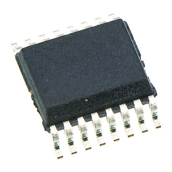
Page 21: Pin Configuration (Top View)
RL78/G10 CHAPTER 1 OUTLINE Note For the fields of application, refer to Figure 1-1 Part Number, Memory Size, and Package of RL78/G10. Caution The part number represents the number at the time of publication. Be sure to review the latest part number through the target product page in the Renesas Electronics Corp.website. -
Page 22: Pin Identification
RL78/G10 CHAPTER 1 OUTLINE 1.4 Pin Identification ANI0 to ANI6 : Analog Input INTP0 to INTP3 : Interrupt Request From Peripherals KR0 to KR5 : Key Return P00 to P07 : Port 0 P40, P41 : Port 4 P121, P122, P125... -
Page 23: Block Diagram
RL78/G10 CHAPTER 1 OUTLINE 1.5 Block Diagram 1.5.1 10-pin products PORT 0 P00 to P04 TAU0 (2 ch) PORT 4 TI00 /TO00 ch00 PORT 12 P125 TI01 /TO01 ch01 PORT 13 P137 Code flash: 4 KB SAU0 (1 ch) RxD0... -
Page 24: 16-Pin Products
RL78/G10 CHAPTER 1 OUTLINE 1.5.2 16-pin products TAU0 (4 ch) ch00 TI00 / TO00 PORT 0 P00 to P07 TI01 / TO01 ch01 PORT 4 P40, P41 TI02 / TO02 ch02 PORT 12 P121, P122, P125 ch03 TI03 / TO03... -
Page 25: Outline Of Functions
RL78/G10 CHAPTER 1 OUTLINE 1.6 Outline of Functions This outline describes the function at the time when Peripheral I/O redirection register (PIOR) is set to 00H. Item 10-pin 16-pin R5F10Y14 R5F10Y16 R5F10Y17 R5F10Y44 R5F10Y46 R5F10Y47 Code flash memory 1 KB... - Page 26 RL78/G10 CHAPTER 1 OUTLINE Item 10-pin 16-pin R5F10Y14 R5F10Y16 R5F10Y17 R5F10Y44 R5F10Y46 R5F10Y47 On-chip debug function Provided Power supply voltage = 2.0 to 5.5 V Note 3 = - 40 to + 85 °C Operating ambient temperature The number of outputs varies, depending on the setting of channels in use and the number of the master Notes 1.
-
Page 27: Chapter 2 Pin Functions
RL78/G10 CHAPTER 2 PIN FUNCTIONS CHAPTER 2 PIN FUNCTIONS 2.1 Port Functions The input or output, buffer, and pull-up resistor settings are also valid for the alternate functions. 2.1.1 10-pin products Function Pin Type After Reset Alternate Function Function Name... -
Page 28: 16-Pin Products
RL78/G10 CHAPTER 2 PIN FUNCTIONS 2.1.2 16-pin products Function Pin Type After Reset Alternate Function Function Name Release 7-1-2 Input port SO00/TXD0/INTP1 Port 0. 8-bit I/O port. Analog input ANI0/SI00/RXD0/ 7-3-2 port Input/output can be specified in 1-bit units. SDA00/KR2... -
Page 29: Functions Other Than Port Pins
RL78/G10 CHAPTER 2 PIN FUNCTIONS 2.2 Functions other than port pins 2.2.1 Functions for each product Function 16-pin 10-pin Function 16-pin 10-pin Name products products Name products products ANI0 √ √ RxD0 √ √ ANI1 √ √ TxD0 √ √... -
Page 30: Description Of Functions
RL78/G10 CHAPTER 2 PIN FUNCTIONS 2.2.2 Description of functions Function Name Functions ANI0 to ANI6 input Analog input pins of A/D converter (See Figure 10-23 Analog Input Pin Connection.) IVCOUT0 output Comparator output IVCMP0 input Analog input for the comparator... -
Page 31: Connection Of Unused Pins
RL78/G10 CHAPTER 2 PIN FUNCTIONS 2.3 Connection of Unused Pins Table 2-2 shows the connections of unused pins. Remark The pins mounted depend on the product. Refer to 1.3 Pin Configuration (Top View) and 2.1 Port Functions. Table 2-2. Connection of Unused Pins... -
Page 32: Block Diagrams Of Pins
RL78/G10 CHAPTER 2 PIN FUNCTIONS 2.4 Block Diagrams of Pins Figures 2-1 to 2-8 show the block diagrams of the pins described in 2.1.1 10-pin products and 2.1.2 16-pin products. Figure 2-1. Pin Block Diagram for Pin Type 2-1-2 Alternate function Remark For alternate functions, see 2.1 Port Functions. - Page 33 RL78/G10 CHAPTER 2 PIN FUNCTIONS Figure 2-2. Pin Block Diagram for Pin Type 2-2-1 Clock generator OSCSEL Alternate function P122/X2/EXCLK/Alternate function EXCLK, OSCSEL N-ch P-ch Alternate function P121/X1/Alternate function R01UH0384EJ0311 Rev. 3.11 Dec 22, 2016...
- Page 34 RL78/G10 CHAPTER 2 PIN FUNCTIONS Figure 2-3. Pin Block Diagram for Pin Type 3-1-1 PU register P-ch (PUmn) Alternate function RESET PORTSELB Remark For alternate functions, see 2.1 Port Functions. R01UH0384EJ0311 Rev. 3.11 Dec 22, 2016...
- Page 35 RL78/G10 CHAPTER 2 PIN FUNCTIONS Figure 2-4. Pin Block Diagram for Pin Type 7-1-1 PU register P-ch (PUmn) Alternate function PORT Output latch (Pmn) P-ch N-ch PM register (PMmn) Alternate function (SAU) Alternate function (other than SAU ) Remarks 1. For alternate functions, see 2.1 Port Functions.
- Page 36 RL78/G10 CHAPTER 2 PIN FUNCTIONS Figure 2-5. Pin Block Diagram for Pin Type 7-1-2 PU register P-ch (PUmn) Alternate function PORT Output latch (Pmn) P-ch N-ch PM register (PMmn) POM register (POMmn) Alternate function (SAU) Alternate function (other than SAU )
- Page 37 RL78/G10 CHAPTER 2 PIN FUNCTIONS Figure 2-6. Pin Block Diagram for Pin Type 7-3-1 PU register (PUmn) P-ch PMC register (PMCmn) Alternate function PORT Output latch (Pmn) P-ch N-ch PM register (PMmn) Alternate function (SAU) Alternate function (other than SAU )
- Page 38 RL78/G10 CHAPTER 2 PIN FUNCTIONS Figure 2-7. Pin Block Diagram for Pin Type 7-3-2 PU register (PUmn) P-ch PMC register (PMCmn) Alternate function PORT Output latch (Pmn) P-ch N-ch PM register (PMmn) POM register (POMmn) Alternate function (SAU) Alternate function...
- Page 39 RL78/G10 CHAPTER 2 PIN FUNCTIONS Figure 2-8. Pin Block Diagram for Pin Type 7-9-1 PU register P-ch (PUmn) PMC register (PMCmn) Alternate function PORT Output latch (Pmn) P-ch N-ch PM register (PMmn) Alternate function (SAU) Alternate function (other than SAU )
-
Page 40: Chapter 3 Cpu Architecture
RL78/G10 CHAPTER 3 CPU ARCHITECTURE CHAPTER 3 CPU ARCHITECTURE The RL78/G10 has the RL78-S1 core. The features of the RL78-S1 core are as follows. • CISC architecture with 3-stage pipeline • Address space: 1 MB • General-purpose register : 8-bit register × 8 •... -
Page 41: Memory Space
RL78/G10 CHAPTER 3 CPU ARCHITECTURE 3.1 Memory Space Products in the RL78/G10 can access a 1 MB address space. Figures 3-1 to 3-3 show the memory maps. Figure 3-1. Memory Map for the R5F10Y14 and R5F10Y44 003FFH FFFFFH Special function register (SFR) - Page 42 RL78/G10 CHAPTER 3 CPU ARCHITECTURE Figure 3-2. Memory Map for the R5F10Y16 and R5F10Y46 007FFH FFFFFH Special function register (SFR) 256 bytes FFF00H FFEFFH General-purpose register 8 bytes FFEF8H FFEF7H Reserved FFEE0H FFEDFH 256 bytes FFDE0H FFDDFH Program area Reserved...
- Page 43 RL78/G10 CHAPTER 3 CPU ARCHITECTURE Figure 3-3. Memory Map for the R5F10Y17 and R5F10Y47 00FFFH FFFFFH Special function register (SFR) 256 bytes FFF00H FFEFFH General-purpose register 8 bytes FFEF8H FFEF7H Reserved FFEE0H FFEDFH 512 bytes FFCE0H FFCDFH Program area Reserved...
-
Page 44: Internal Program Memory Space
CHAPTER 3 CPU ARCHITECTURE 3.1.1 Internal program memory space The internal program memory space stores the program and table data. The RL78/G10 products incorporate internal ROM (flash memory), as shown below. Table 3-1. Internal ROM Capacity Part Number Internal ROM... - Page 45 RL78/G10 CHAPTER 3 CPU ARCHITECTURE (2) CALLT instruction table area The 64-byte area of 00080H to 000BFH can store the subroutine entry address of a 2-byte call instruction (CALLT). Set the subroutine entry address to a value in a range of 00000H to 0FFFFH (because an address code is 2 bytes).
-
Page 46: Mirror Area
RL78/G10 CHAPTER 3 CPU ARCHITECTURE 3.1.2 Mirror area <R> The products with 1/2/4 KB flash memory mirror the code flash area of 00000H to 003FFH/007FFH/00FFFH to the area of F8000H to F83FFH/F87FFH/F8FFFH (the code flash area to be mirrored is set by the processor mode control register (PMC)). -
Page 47: Internal Data Memory Space
RL78/G10 CHAPTER 3 CPU ARCHITECTURE 3.1.3 Internal data memory space The RL78/G10 products incorporate the following RAMs. Table 3-3. Internal RAM Capacity Part Number Internal RAM R5F10Y14, R5F10Y44 128 bytes (FFE60H to FFEDFH) R5F10Y16, R5F10Y46 256 bytes (FFDE0H to FFEDFH) -
Page 48: Data Memory Addressing
Several addressing modes are provided for addressing the memory relevant to the execution of instructions for the RL78/G10, based on operability and other considerations. For areas containing data memory in particular, special addressing methods designed for the functions of the special function registers (SFR) and general-purpose registers are available for use. -
Page 49: Processor Registers
RL78/G10 CHAPTER 3 CPU ARCHITECTURE 3.2 Processor Registers The RL78/G10 products incorporate the following processor registers. 3.2.1 Control registers The control registers control the program sequence, statuses and stack memory. The control registers consist of a program counter (PC), a program status word (PSW) and a stack pointer (SP). - Page 50 RL78/G10 CHAPTER 3 CPU ARCHITECTURE (d) In-service priority flags (ISP1, ISP0) These flags manage the priority of acknowledgeable maskable vectored interrupts. Vectored interrupt requests specified lower than the value of ISP0 and ISP1 flags by the priority specification flag registers (PR00L, PR00H, PR10L, PR10H, PR01L, PR11L) (see 14.3.3 Priority specification flag registers (PR00L, PR00H, PR10L,...
-
Page 51: General-Purpose Registers
RL78/G10 CHAPTER 3 CPU ARCHITECTURE 3.2.2 General-purpose registers The general-purpose registers are a bank of eight 8-bit registers (X, A, C, B, E, D, L, and H) mapped to addresses (FFEF8H to FFEFFH) of the data memory. Each register can be used as an 8-bit register, and two 8-bit registers can also be used in a pair as a 16-bit register (AX, BC, DE, and HL). -
Page 52: Es And Cs Registers
RL78/G10 CHAPTER 3 CPU ARCHITECTURE 3.2.3 ES and CS registers The ES register and CS register are used to specify the higher address for data access and when a branch instruction is executed (register direct addressing), respectively. The default value of the ES register after reset is 0FH, and that of the CS register is 00H. -
Page 53: Special Function Registers (Sfrs)
RL78/G10 CHAPTER 3 CPU ARCHITECTURE 3.2.4 Special function registers (SFRs) Unlike a general-purpose register, each SFR has a special function. SFRs are allocated to the FFF00H to FFFFFH area. SFRs can be manipulated like general-purpose registers, using operation, transfer, and bit manipulation instructions. - Page 54 RL78/G10 CHAPTER 3 CPU ARCHITECTURE Table 3-4. SFR List (1/2) Address Special Function Register (SFR) Name Symbol Manipulable Bit Range After Reset 1-bit 8-bit FFF00H Port register 0 √ √ √ √ FFF04H Port register 4 √ √ FFF0CH Port register 12 Undefined √...
- Page 55 RL78/G10 CHAPTER 3 CPU ARCHITECTURE Table 3-4. SFR List (2/2) Address Special Function Register (SFR) Name Symbol Manipulable Bit Range After Reset 1-bit 8-bit Note 1 FFFA0H Clock operation mode control register − √ Clock operation status control register Note 1 √...
-
Page 56: Extended Special Function Registers (2Nd Sfrs: 2Nd Special Function Registers)
RL78/G10 CHAPTER 3 CPU ARCHITECTURE 3.2.5 Extended special function registers (2nd SFRs: 2nd Special Function Registers) Unlike a general-purpose register, each extended SFR (2nd SFR) has a special function. Extended SFRs are allocated to the F0000H to F07FFH area. SFRs other than those in the SFR area (FFF00H to FFFFFH) are allocated to this area. - Page 57 RL78/G10 CHAPTER 3 CPU ARCHITECTURE Table 3-5. Extended SFR (2nd SFR) List (1/2) Address Special Function Register (SFR) Name Symbol Manipulable Bit Range After Reset 1-bit 8-bit F0010H A/D converter mode register 2 ADM2 √ √ <R> Note 1 −...
- Page 58 RL78/G10 CHAPTER 3 CPU ARCHITECTURE Table 3-5. Extended SFR (2nd SFR) List (2/2) Address Special Function Register (SFR) Name Symbol Manipulable Bit Range After Reset 1-bit 8-bit Note F0184H Timer counter register 02L TCR02L − √ F0185H Timer counter register 02H...
-
Page 59: Instruction Address Addressing
RL78/G10 CHAPTER 3 CPU ARCHITECTURE 3.3 Instruction Address Addressing 3.3.1 Relative addressing [Function] Relative addressing stores in the program counter (PC) the result of adding a displacement value included in the instruction word (signed complement data: −128 to +127 or −32768 to +32767) to the program counter (PC)’s value (the start address of the next instruction), and specifies the program address to be used as the branch destination. -
Page 60: Register Direct Addressing
RL78/G10 CHAPTER 3 CPU ARCHITECTURE 3.3.3 Table indirect addressing [Function] Table indirect addressing specifies a table address in the CALLT table area (0080H to 00BFH) with the 5-bit immediate data in the instruction word, stores the contents at that table address and the next address in the program counter (PC) as 16-bit data, and specifies the program address. -
Page 61: Addressing For Processing Data Addresses
RL78/G10 CHAPTER 3 CPU ARCHITECTURE 3.4 Addressing for Processing Data Addresses 3.4.1 Implied addressing [Function] Instructions for accessing registers (such as accumulators) that have special functions are directly specified with the instruction word, without using any register specification field in the instruction word. -
Page 62: Direct Addressing
RL78/G10 CHAPTER 3 CPU ARCHITECTURE 3.4.3 Direct addressing [Function] Direct addressing uses immediate data in the instruction word as an operand address to directly specify the target address. [Operand format] Identifier Description !addr16 Label or 16-bit immediate data (only the space from F0000H to FFFFFH is specifiable) -
Page 63: Short Direct Addressing
RL78/G10 CHAPTER 3 CPU ARCHITECTURE 3.4.4 Short direct addressing [Function] Short direct addressing directly specifies the target addresses using 8-bit data in the instruction word. This type of addressing is applied only to the space from FFE20H to FFF1FH. Note that it is prohibited to use the area from FFEE0H to FFEF7H. In the products with 128 bytes of RAM, it is also prohibited to use the area from FFE20H to FFE5FH. -
Page 64: Sfr Addressing
RL78/G10 CHAPTER 3 CPU ARCHITECTURE 3.4.5 SFR addressing [Function] SFR addressing directly specifies the target SFR addresses using 8-bit data in the instruction word. This type of addressing is applied only to the space from FFF00H to FFFFFH. [Operand format]... -
Page 65: Register Indirect Addressing
RL78/G10 CHAPTER 3 CPU ARCHITECTURE 3.4.6 Register indirect addressing [Function] Register indirect addressing directly specifies the target addresses using the contents of the register pair specified with the instruction word as an operand address. [Operand format] Identifier Description − [DE], [HL] (only the space from F0000H to FFFFFH is specifiable) −... -
Page 66: Based Addressing
RL78/G10 CHAPTER 3 CPU ARCHITECTURE 3.4.7 Based addressing [Function] Based addressing uses the contents of a register pair specified with the instruction word or 16-bit immediate data as a base address, and 8-bit immediate data or 16-bit immediate data as offset data. The sum of these values is used to specify the target address. - Page 67 RL78/G10 CHAPTER 3 CPU ARCHITECTURE Figure 3-25. Example of [HL + byte], [DE + byte] [HL + byte], [DE + byte] <1> <2> <1> <2> FFFFFH Instruction code Target OP-code Target memory array <2> Offset of data <2> byte <1>...
- Page 68 RL78/G10 CHAPTER 3 CPU ARCHITECTURE Figure 3-28. Example of ES:[HL + byte], ES:[DE + byte] ES: [HL + byte], ES: [DE + byte] <1> <2> <3> <1> <2> <3> XFFFFH Instruction code <2> Target memory <3> Target OP-code array Offset...
- Page 69 RL78/G10 CHAPTER 3 CPU ARCHITECTURE Figure 3-30. Example of ES:word[BC] ES: word [BC] <1> <2> <3> XFFFFH Array of Instruction code Target memory <3> word-sized <3> Offset data OP-code rp(BC) <2> Low Addr. Address of a word within an array <2>...
-
Page 70: Based Indexed Addressing
RL78/G10 CHAPTER 3 CPU ARCHITECTURE 3.4.8 Based indexed addressing [Function] Based indexed addressing uses the contents of a register pair specified with the instruction word as the base address, and the content of the B register or C register similarly specified with the instruction word as offset address. -
Page 71: Stack Addressing
RL78/G10 CHAPTER 3 CPU ARCHITECTURE 3.4.9 Stack addressing [Function] The stack area is indirectly addressed with the stack pointer (SP) values. This addressing is automatically employed when the PUSH, POP, subroutine call, and return instructions are executed or the register is saved/restored upon generation of an interrupt request. - Page 72 RL78/G10 CHAPTER 3 CPU ARCHITECTURE Figure 3-34. Example of POP POP rp <1> <2> SP + 2 <1> SP + 1 Stack (SP+1) Instruction code area (SP) <2> OP-code F0000H Stack addressing is specified <1>. The contents of addresses SP and SP + 1 are stored in the lower-order and higher-order bytes of the pair of registers indicated by rp <2>, respectively.
- Page 73 RL78/G10 CHAPTER 3 CPU ARCHITECTURE Figure 3-36. Example of RET <1> SP+4 <1> SP+3 (SP+3) Instruction code Stack SP+2 (SP+2) OP-code area SP+1 (SP+1) <3> (SP) <2> F0000H Stack addressing is specified <1>. The contents of addresses SP, SP + 1, and SP + 2 are stored in PC bits 7 to 0, 15 to 8, and 19 to 16, respectively <2>.
- Page 74 RL78/G10 CHAPTER 3 CPU ARCHITECTURE Figure 3-38. Example of RETI, RETB RETI, RETB <1> SP+4 <1> SP+3 (SP+3) Instruction code SP+2 (SP+2) Stack OP-code area SP+1 (SP+1) <3> (SP) <2> F0000H Stack addressing is specified <1>. Memory The contents of addresses SP, SP + 1, SP + 2, and SP + 3 are stored in PC bits 7 to 0, 15 to 8, 19 to 16, and the PSW, respectively <2>.
-
Page 75: Chapter 4 Port Functions
RL78/G10 CHAPTER 4 PORT FUNCTIONS CHAPTER 4 PORT FUNCTIONS 4.1 Port Functions The RL78 microcontrollers are provided with digital I/O ports, which enable variety of control operations. In addition to the function as digital I/O ports, these ports have several alternate functions. For details of the alternate functions, see CHAPTER 2 PIN FUNCTIONS. -
Page 76: Port 0
RL78/G10 CHAPTER 4 PORT FUNCTIONS 4.2.1 Port 0 Port 0 is an I/O port with output latches. Port 0 can be set to the input mode or output mode in 1-bit units using port Note mode register 0 (PM0). When the P00 to P07 pins are used as input pins, use of the on-chip pull-up resistors can be specified in 1-bit units by pull-up resistor option register 0 (PU0). -
Page 77: Registers Controlling Port Function
RL78/G10 CHAPTER 4 PORT FUNCTIONS 4.3 Registers Controlling Port Function Port functions are controlled by the following registers. • Port mode registers 0, 4 (PM0, PM4) • Port registers 0, 4, 12, 13 (P0, P4, P12, P13) • Pull-up resistor option registers 0, 4, 12 (PU0, PU4, PU12) •... -
Page 78: Port Mode Registers 0, 4 (Pm0, Pm4)
RL78/G10 CHAPTER 4 PORT FUNCTIONS 4.3.1 Port mode registers 0, 4 (PM0, PM4) These registers specify input or output mode for the port in 1-bit units. These registers can be set by a 1-bit or 8-bit memory manipulation instruction. Reset signal generation sets these registers to FFH. -
Page 79: Port Registers 0, 4, 12, 13 (P0, P4, P12, P13)
RL78/G10 CHAPTER 4 PORT FUNCTIONS 4.3.2 Port registers 0, 4, 12, 13 (P0, P4, P12, P13) These registers set the output latch value of a port. If the data is read in the input mode, the pin level is read. If it is read in the output mode, the output latch value is... -
Page 80: Pull-Up Resistor Option Registers 0, 4, 12 (Pu0, Pu4, Pu12)
RL78/G10 CHAPTER 4 PORT FUNCTIONS 4.3.3 Pull-up resistor option registers 0, 4, 12 (PU0, PU4, PU12) These registers specify whether the on-chip pull-up resistors are to be used or not. On-chip pull-up resistors can be used in 1-bit units only for the bits that satisfy the following usage conditions for the pins to which the use of an on-chip pull-up resistor has been specified in these registers. -
Page 81: Port Output Mode Register 0 (Pom0)
RL78/G10 CHAPTER 4 PORT FUNCTIONS 4.3.4 Port output mode register 0 (POM0) This register sets CMOS output or N-ch open drain output in 1-bit units. N-ch open drain output (V tolerant) mode can be selected for the SDA00 pin during simplified I C communication with an external device. -
Page 82: Port Mode Control Register 0 (Pmc0)
RL78/G10 CHAPTER 4 PORT FUNCTIONS 4.3.5 Port mode control register 0 (PMC0) This register sets the digital I/O or analog input in 1-bit units. This register can be set by a 1-bit or 8-bit memory manipulation instruction. Reset signal generation sets this register to FFH. -
Page 83: Peripheral I/O Redirection Register (Pior)
RL78/G10 CHAPTER 4 PORT FUNCTIONS 4.3.6 Peripheral I/O redirection register (PIOR) This register is used to specify whether to enable or disable the peripheral I/O redirect function. This function is used to switch ports to which alternate functions are assigned. -
Page 84: Port Function Operations
RL78/G10 CHAPTER 4 PORT FUNCTIONS 4.4 Port Function Operations Port operations differ depending on whether the input or output mode is set, as shown below. 4.4.1 Writing to I/O port (1) Output mode A value is written to the output latch by a transfer instruction, and the output latch contents are output from the pin. -
Page 85: Register Settings When An Alternate Function Is Used
RL78/G10 CHAPTER 4 PORT FUNCTIONS 4.5 Register Settings When an Alternate Function Is Used 4.5.1 Basic concepts on using an alternate function If a given pin is also used alternately for analog input, first in the port mode control register 0 (PMC0) specify whether the pin is to be used in analog input or digital output. -
Page 86: Register Settings For Alternate Functions That Do Not Use An Output Function
RL78/G10 CHAPTER 4 PORT FUNCTIONS 4.5.2 Register settings for alternate functions that do not use an output function If the output from an alternate function associated with a pin is not used, the settings described below must be specified. If the pin is subject to a peripheral I/O redirect function, the output can be changed to another pin by setting the peripheral I/O redirection register (PIOR). - Page 87 RL78/G10 CHAPTER 4 PORT FUNCTIONS Table 4-5. Examples of Register And Output Latch Settings With Pin Functions (1/4) Function PIOR POM0 PMC0 Alternate function output pins pins Name SAU output Non-SAU function − × − × × − √ √...
- Page 88 RL78/G10 CHAPTER 4 PORT FUNCTIONS Table 4-5. Examples of Register And Output Latch Settings With Pin Functions (2/4) Function PIOR POM0 PMC0 Alternate function output pins pins Name SAU output Non-SAU function − − × × × √ − Input −...
- Page 89 RL78/G10 CHAPTER 4 PORT FUNCTIONS Table 4-5. Examples of Register And Output Latch Settings With Pin Functions (3/4) Function PIOR POM0 PMC0 (EXCLK,OSCSEL) pins pins Name − − − − × − √ P121 P121 Input 00/10/11 − − −...
-
Page 90: Cautions When Using Port Function
RL78/G10 CHAPTER 4 PORT FUNCTIONS 4.6 Cautions When Using Port Function 4.6.1 Cautions on 1-bit manipulation instruction for port register n (Pn) When a 1-bit manipulation instruction is executed on a port that provides both input and output functions, the output latch value of an input port that is not subject to manipulation may be written in addition to the targeted bit. -
Page 91: Notes On Specifying The Pin Settings
RL78/G10 CHAPTER 4 PORT FUNCTIONS 4.6.2 Notes on specifying the pin settings For an output pin to which multiple alternate functions are assigned, the output of the unused alternate functions must be set to its initial state so as to prevent conflicting outputs. This also applies to the functions assigned by using the peripheral I/O redirection register (PIOR). -
Page 92: Chapter 5 Clock Generator
RL78/G10 CHAPTER 5 CLOCK GENERATOR CHAPTER 5 CLOCK GENERATOR 5.1 Functions of Clock Generator The clock generator generates the clock to be supplied to the CPU and peripheral hardware. The following three kinds of system clocks and clock oscillators are selectable. -
Page 93: Configuration Of Clock Generator
RL78/G10 CHAPTER 5 CLOCK GENERATOR (2) Low Speed On-chip Oscillator clock This circuit oscillates a clock of f = 15 kHz (typ.). The low speed on-chip oscillator clock cannot be used as the CPU clock. Only the following peripheral hardware runs on the low speed on-chip oscillator clock. - Page 94 RL78/G10 CHAPTER 5 CLOCK GENERATOR R01UH0384EJ0311 Rev. 3.11 Dec 22, 2016...
-
Page 95: Registers Controlling Clock Generator
RL78/G10 CHAPTER 5 CLOCK GENERATOR Remark f X1 clock oscillation frequency High-speed on-chip oscillator clock frequency External main system clock frequency High-speed system clock frequency Main system clock frequency MAIN CPU/peripheral hardware clock frequency Low-speed on-chip oscillator clock frequency 5.3 Registers Controlling Clock Generator The clock generator is controlled by the following registers depending on the products. -
Page 96: Clock Operation Mode Control Register (Cmc)
RL78/G10 CHAPTER 5 CLOCK GENERATOR 5.3.1 Clock operation mode control register (CMC) This register is used to set the operation mode of the X1/P121/(INTP3) and X2/EXCLK/P122/(INTP2) pins, and to select a gain of the oscillator. The CMC register can be written only once by an 8-bit memory manipulation instruction after reset release. This register can be read by an 8-bit memory manipulation instruction. -
Page 97: System Clock Control Register (Ckc)
RL78/G10 CHAPTER 5 CLOCK GENERATOR 5.3.2 System clock control register (CKC) This register is used to select a main system clock. The CKC register can be set by a 1-bit or 8-bit memory manipulation instruction. Reset signal generation sets this register to 00H. -
Page 98: Clock Operation Status Control Register (Csc)
RL78/G10 CHAPTER 5 CLOCK GENERATOR 5.3.3 Clock operation status control register (CSC) This register is used to control the operations of the high-speed system clock and high-speed on-chip oscillator clock, (except the low-speed on-chip oscillator clock). The CSC register can be set by a 1-bit or 8-bit memory manipulation instruction. -
Page 99: Oscillation Stabilization Time Counter Status Register (Ostc)
RL78/G10 CHAPTER 5 CLOCK GENERATOR 5.3.4 Oscillation stabilization time counter status register (OSTC) This is the register that indicates the count status of the X1 clock oscillation stabilization time counter. The X1 clock oscillation stabilization time can be checked in the following case: •... - Page 100 RL78/G10 CHAPTER 5 CLOCK GENERATOR 3. The X1 clock oscillation stabilization wait time does not include the time until clock oscillation starts (“a” below). STOP mode release X1 pin voltage waveform Remark f : X1 clock oscillation frequency R01UH0384EJ0311 Rev. 3.11...
-
Page 101: Oscillation Stabilization Time Select Register (Osts)
RL78/G10 CHAPTER 5 CLOCK GENERATOR 5.3.5 Oscillation stabilization time select register (OSTS) This register is used to select the X1 clock oscillation stabilization wait time when the STOP mode is released. When the X1 clock is selected as the CPU clock, the operation automatically waits for the time set using the OSTS register after the STOP mode is released. -
Page 102: Peripheral Enable Register 0 (Per0)
RL78/G10 CHAPTER 5 CLOCK GENERATOR 5.3.6 Peripheral enable register 0 (PER0) This register is used to enable or disable supplying the clock to the peripheral hardware. Clock supply to the hardware that is not used is also stopped so as to decrease the power consumption and noise. -
Page 103: Operation Speed Mode Control Register (Osmc)
RL78/G10 CHAPTER 5 CLOCK GENERATOR Figure 5-7. Format of Peripheral Enable Register 0 (PER0) (2/2) Address: F00F0H After reset: 00H Symbol <7> <6> <5> <4> <2> <0> PER0 TMKAEN CMPEN ADCEN IICA0EN SAU0EN TAU0EN Note Note Note IICA0EN Control of serial interface IICA input clock supply Stops input clock supply. -
Page 104: High-Speed On-Chip Oscillator Frequency Selection Register (Hocodiv)
RL78/G10 CHAPTER 5 CLOCK GENERATOR 5.3.8 High-speed on-chip oscillator frequency selection register (HOCODIV) This register is used to change the frequency of the high-speed on-chip oscillator clock set with the option byte (000C2H). HOCODIV can be set by an 8-bit memory manipulation instruction. -
Page 105: System Clock Oscillator
RL78/G10 CHAPTER 5 CLOCK GENERATOR 5.4 System Clock Oscillator 5.4.1 X1 oscillator (16-pin products only) The X1 oscillator oscillates with a crystal resonator or ceramic resonator (1 to 20 MHz) connected to the X1 and X2 pins. An external clock can be input. In that case, input the clock signal to the EXCLK pin. - Page 106 RL78/G10 CHAPTER 5 CLOCK GENERATOR Figure 5-11 shows examples of incorrect resonator connection. Figure 5-11. Examples of Incorrect Resonator Connection (1/2) (a) Too long wiring (b) Crossed signal line PORT (c) The X1 and X2 signal line wires cross. (d) A power supply/GND pattern exists under the X1 and X2 wires.
- Page 107 RL78/G10 CHAPTER 5 CLOCK GENERATOR Figure 5-11. Examples of Incorrect Resonator Connection (2/2) (e) Wiring near high alternating current (f) Current flowing through ground line of oscillator (potential at points A, B, and C fluctuates) High current (g) Signals are fetched R01UH0384EJ0311 Rev.
-
Page 108: High-Speed On-Chip Oscillator
5.4.2 High-speed on-chip oscillator The high-speed on-chip oscillator is incorporated in the RL78/G10. The frequency can be selected from among 20, 10, 5, 2.5, or 1.25 MHz by using the option byte (000C2H). Oscillation can be controlled by bit 0 (HIOSTOP) of the clock... - Page 109 RL78/G10 CHAPTER 5 CLOCK GENERATOR Figure 5-12. Clock Generator Operation When Power Supply Voltage Is Turned On Power supply voltage (V SPOR release reset voltage <1> Internal reset signal Switched by software SPOR reset Note 3 processing <3> <5> CPU clock...
-
Page 110: Controlling Clock
RL78/G10 CHAPTER 5 CLOCK GENERATOR 5.6 Controlling Clock 5.6.1 Example of setting high-speed on-chip oscillator After a reset release, the CPU/peripheral hardware clock (f ) always starts operating with the high-speed on-chip oscillator clock. The frequency of the high-speed on-chip oscillator can be selected by using FRQSEL0 to FRQSEL2 of the option byte (000C2H). -
Page 111: Example Of Setting X1 Oscillation Clock
RL78/G10 CHAPTER 5 CLOCK GENERATOR 5.6.2 Example of setting X1 oscillation clock After a reset release, the CPU/peripheral hardware clock (f ) always starts operating with the high-speed on-chip oscillator clock. To subsequently change the clock to the X1 clock, set the oscillator and start oscillation by using the... -
Page 112: Cpu Clock Status Transition Diagram
RL78/G10 CHAPTER 5 CLOCK GENERATOR 5.6.3 CPU clock status transition diagram Figure 5-13 shows the CPU clock status transition diagram of this product. Figure 5-13. CPU Clock Status Transition Diagram Power ON High-speed on-chip oscillator: Woken up X1 oscillation/EXCLK input: Stops (input port mode) being greater than the detection voltage for the SPOR circuit and release from the reset state due to any reset source. - Page 113 RL78/G10 CHAPTER 5 CLOCK GENERATOR Table 5-3 shows transition of the CPU clock and examples of setting the SFR registers. Table 5-3. CPU Clock Transition and SFR Register Setting Examples (1/2) (1) CPU clock changing from high-speed on-chip oscillator clock (A) to high-speed system clock (B) (The CPU operates with the high-speed on-chip oscillator clock immediately after a reset release (A).)
- Page 114 RL78/G10 CHAPTER 5 CLOCK GENERATOR Table 5-3. CPU Clock Transition and SFR Register Setting Examples (2/2) (2) CPU clock changing from high-speed system clock (B) to high-speed on-chip oscillator clock (A) (Setting sequence of SFR registers) Setting Flag of SFR Register...
-
Page 115: Condition Before Changing Cpu Clock And Processing After Changing Cpu Clock
RL78/G10 CHAPTER 5 CLOCK GENERATOR 5.6.4 Condition before changing CPU clock and processing after changing CPU clock Condition before changing the CPU clock and processing after changing the CPU clock are shown below. Table 5-4. Changing CPU Clock CPU Clock... -
Page 116: Time Required For Switchover Of Cpu Clock And Main System Clock
RL78/G10 CHAPTER 5 CLOCK GENERATOR 5.6.5 Time required for switchover of CPU clock and main system clock The main system clock can be switched between the high-speed on-chip oscillator clock and the high-speed system clock by specifying bit 4 (MCM0) of the system clock control register (CKC). -
Page 117: Resonator And Oscillator Constants
RL78/G10 CHAPTER 5 CLOCK GENERATOR 5.7 Resonator and Oscillator Constants The resonators for which the operation is verified and their oscillator constants are shown below. Cautions 1. The constants for these oscillator circuits are reference values based on specific environments set up for evaluation by the manufacturers. - Page 118 RL78/G10 CHAPTER 5 CLOCK GENERATOR (1) X1 oscillation: As of December, 2013 Manufacturer Resonator Part Number SMD/ Frequency Recommended Circuit Constants Oscillation Voltage Lead (MHz) (reference) Range (V) Note 1 C1 (pF) C2 (pF) Rd (kΩ) MIN. MAX. Murata Crystal...
-
Page 119: Chapter 6 Timer Array Unit
RL78/G10 CHAPTER 6 TIMER ARRAY UNIT CHAPTER 6 TIMER ARRAY UNIT The number of units or channels of the timer array unit differs, depending on the product. Channel 10-pin 16-pin Channel 0 √ √ √ √ Channel 1 Channel 2 −... - Page 120 RL78/G10 CHAPTER 6 TIMER ARRAY UNIT For details about each function, see the table below. Independent channel operation function Simultaneous channel operation function • One-shot pulse output (→ refer to 6.9.1) • Interval timer (→ refer to 6.8.1) • Square wave output (→ refer to 6.8.1) •...
-
Page 121: Functions Of Timer Array Unit
RL78/G10 CHAPTER 6 TIMER ARRAY UNIT 6.1 Functions of Timer Array Unit Timer array unit has the following functions. 6.1.1 Independent channel operation function By operating a channel independently, it can be used for the following purposes without being affected by the operation mode of other channels. - Page 122 RL78/G10 CHAPTER 6 TIMER ARRAY UNIT (6) Measurement of high-/low-level width of input signal Counting is started by a single edge of the signal input to the timer input pin (TI0n), and the count value is captured at the other edge. In this way, the high-level or low-level width of the input signal can be measured.
-
Page 123: Simultaneous Channel Operation Function
RL78/G10 CHAPTER 6 TIMER ARRAY UNIT 6.1.2 Simultaneous channel operation function By using the combination of a master channel (a reference timer mainly controlling the cycle) and a slave channel (a timer operating according to the master channel), channels can be used for the following purposes. - Page 124 RL78/G10 CHAPTER 6 TIMER ARRAY UNIT (3) PWM (Pulse Width Modulation) output function Two channels are used as a set to generate a pulse with a specified period and a specified duty factor. Compare operation Operation clock Interrupt request signal...
-
Page 125: 8-Bit Timer Operation Function (Channels 1 And 3 Only)
RL78/G10 CHAPTER 6 TIMER ARRAY UNIT 6.1.3 8-bit timer operation function (channels 1 and 3 only) The 8-bit timer operation function makes it possible to use a 16-bit timer in a configuration consisting of two 8-bit timers (higher and lower). -
Page 126: Configuration Of Timer Array Unit
RL78/G10 CHAPTER 6 TIMER ARRAY UNIT 6.2 Configuration of Timer Array Unit Timer array unit includes the following hardware. Table 6-1. Configuration of Timer Array Unit Item Configuration Timer/counter Timer counter register 0n (TCR0nH, TCR0nL) Register Timer data register 0n (TDR0nH, TDR0nL) - Page 127 RL78/G10 CHAPTER 6 TIMER ARRAY UNIT Figures 6-1 and 6-2 show the block diagrams of the timer array unit. Figure 6-1. Entire Configuration of Timer Array Unit Timer clock select register 0 (TPS0) PRS013 PRS012 PRS011 PRS010 PRS003 PRS002 PRS001 PRS000...
- Page 128 RL78/G10 CHAPTER 6 TIMER ARRAY UNIT Figure 6-2. Internal Block Diagram of Channel of Timer Array Unit (a) Channels 0 and 2 Note 1 Interrupt signal from master channel CK00 Timer controller Output TCLK TO00 controller Note 2 CK01 TO02...
- Page 129 RL78/G10 CHAPTER 6 TIMER ARRAY UNIT Note (c) Channel 3 Interrupt signal from master channel Timer controller Output CK00 TCLK TO03 controller CK01 Output latch Mode (Pxx) PMxx selection Interrupt INTTM0n controller Edge (Timer interrupt) TI03 detection Timer counter register 03 (TCR03)
-
Page 130: Timer Counter Register 0N (Tcr0N)
RL78/G10 CHAPTER 6 TIMER ARRAY UNIT 6.2.1 Timer counter register 0n (TCR0n) TCR0n register consists of two 8-bit read-only registers (TCR0nH and TCR0nL) and is used to count clocks (f TCLK When data is read from the TCR0n register, the TCR0nH and TCR0nL registers must be accessed consecutively. - Page 131 RL78/G10 CHAPTER 6 TIMER ARRAY UNIT The TCR0n register read value differs as follows according to operation mode changes and the operating status. Table 6-3. Timer Counter Register 0n (TCR0n) Read Value in Various Operation Modes Note Operation Mode Count Mode...
-
Page 132: Timer Data Register 0N (Tdr0N)
RL78/G10 CHAPTER 6 TIMER ARRAY UNIT 6.2.2 Timer data register 0n (TDR0n) The TDR0n register consists of two eight bit registers (TDR0nH, TDR0nL) for which the capture or comparison functions can be selected. Switching between the capture and comparison functions is by using the MD0n3 to MD0n0 bits of the timer mode register 0n (TMR0n) to select the operating mode. - Page 133 RL78/G10 CHAPTER 6 TIMER ARRAY UNIT Figure 6-4. Format of Timer Data Register 0n (TDR0nH, TDR0nL) (n = 0, 2) Address: FFF18H (TDR00L), FFF19H (TDR00H), After reset: 00H FFF64H (TDR02L), FFF65H (TDR02H) FFF19H (TDR00H) FFF18H (TDR00L) TDR0n Figure 6-5. Format of Timer Data Register 0n (TDR0n) (n = 1, 3)
-
Page 134: Registers Controlling Timer Array Unit
RL78/G10 CHAPTER 6 TIMER ARRAY UNIT 6.3 Registers Controlling Timer Array Unit Timer array unit is controlled by the following registers. • Peripheral enable register 0 (PER0) • Timer clock select register 0 (TPS0) • Timer channel enable status register 0 (TE0, TEH0) •... -
Page 135: Peripheral Enable Register 0 (Per0)
RL78/G10 CHAPTER 6 TIMER ARRAY UNIT 6.3.1 Peripheral enable register 0 (PER0) This registers is used to enable or disable supplying the clock to the peripheral hardware. Clock supply to a hardware macro that is not used is stopped in order to reduce the power consumption and noise. -
Page 136: Timer Clock Select Register 0 (Tps0)
RL78/G10 CHAPTER 6 TIMER ARRAY UNIT 6.3.2 Timer clock select register 0 (TPS0) The TPS0 register is a 16-bit register that is used to select four types of operation clocks (CK00, CK01) that are commonly supplied to each channel from the prescaler. -
Page 137: Timer Mode Register 0N (Tmr0N)
RL78/G10 CHAPTER 6 TIMER ARRAY UNIT 6.3.3 Timer mode register 0n (TMR0n) The TMR0n register consists of two eight-bit registers (TMR0nH, TMR0nL) which set an operation mode of channel n. This register is used to select the operation clock (f... - Page 138 RL78/G10 CHAPTER 6 TIMER ARRAY UNIT Figure 6-8. Format of Timer Mode Register 0n (TMR0n) (1/3) Address: : F0190H (TMR00L), F0191H (TMR00H) After reset: 00H : F0192H (TMR01L), F0193H (TMR01H) : F0194H (TMR02L), F0195H (TMR02H) : F0196H (TMR03L), F0197H (TMR03H)
- Page 139 RL78/G10 CHAPTER 6 TIMER ARRAY UNIT Figure 6-8. Format of Timer Mode Register 0n (TMR0n) (2/3) Symbol TMR00H CKS001 CCS00 STS002 STS001 STS000 Symbol TMR02H CKS021 CCS02 MASTER02 STS022 STS021 STS020 Symbol TMR0nH CKS0n1 CCS0n SPLIT0n STS0n2 STS0n1 STS0n0 (n = 1, 3)
- Page 140 RL78/G10 CHAPTER 6 TIMER ARRAY UNIT Figure 6-8. Format of Timer Mode Register 0n (TMR0n) (3/3) Symbol TMR0nL CIS0n1 CIS0n0 MD0n3 MD0n2 MD0n1 MD0n0 (n = 0 to 3) CIS0n1 CIS0n0 Selection of TI0n pin input valid edge Falling edge...
- Page 141 RL78/G10 CHAPTER 6 TIMER ARRAY UNIT Notes 1. In one-count mode, the interrupt request signal (INTTM0n) when starting a count operation and TO0n output are not controlled. 2. If the start trigger (TS0n = 1) is issued during operation, the counter is initialized, and recounting is started (interrupt request signal (INTTM0n) is not generated).
-
Page 142: Timer Status Register 0N (Tsr0N)
RL78/G10 CHAPTER 6 TIMER ARRAY UNIT 6.3.4 Timer status register 0n (TSR0n) The TSR0n register indicates the overflow status of the counter of channel n. The TSR0n register is valid only in the capture mode (MD0n3 to MD0n1 = 010B) and capture & one-count mode (MD0n3 to MD0n1 = 110B). -
Page 143: Timer Channel Enable Status Register 0 (Te0, Teh0 (8-Bit Mode))
RL78/G10 CHAPTER 6 TIMER ARRAY UNIT 6.3.5 Timer channel enable status register 0 (TE0, TEH0 (8-bit mode)) The TE0 and TEH0 registers are used to enable or stop the timer operation of each channel. Each bit of the TE0 and TEH0 registers correspond to each bit of the timer channel start register 0 (TS0, TSH0) and the timer channel stop register 0 (TT0, TTH0). -
Page 144: Timer Channel Start Register 0 (Ts0, Tsh0 (8-Bit Mode))
RL78/G10 CHAPTER 6 TIMER ARRAY UNIT 6.3.6 Timer channel start register 0 (TS0, TSH0 (8-bit mode)) The TS0 and TSH0 registers are trigger registers that are used to initialize timer counter register 0n (TCR0n) and start the counting operation of each channel. -
Page 145: Timer Channel Stop Register 0 (Tt0, Tth0 (8-Bit Mode))
RL78/G10 CHAPTER 6 TIMER ARRAY UNIT 6.3.7 Timer channel stop register 0 (TT0, TTH0 (8-bit mode)) The TT0 and TTH0 registers are trigger registers that are used to stop the counting operation of each channel. When a bit of TT0 and TTH0 registers is set to 1, the corresponding bit of timer channel enable status register 0 (TE0, TEH0) is cleared to 0. -
Page 146: Timer Output Enable Register 0 (Toe0)
RL78/G10 CHAPTER 6 TIMER ARRAY UNIT 6.3.8 Timer output enable register 0 (TOE0) The TOE0 register is used to enable or disable timer output of each channel. Channel n for which timer output has been enabled becomes unable to rewrite the value of the TO0n bit of timer output register 0 (TO0) described later by software, and the value reflecting the setting of the timer output function through the count operation is output from the timer output pin (TO0n). -
Page 147: Timer Output Register 0 (To0)
RL78/G10 CHAPTER 6 TIMER ARRAY UNIT 6.3.9 Timer output register 0 (TO0) The TO0 register is a buffer register of timer output of each channel. The value of each bit in this register is output from the timer output pin (TO0n) of each channel. -
Page 148: Timer Output Level Register 0 (Tol0)
RL78/G10 CHAPTER 6 TIMER ARRAY UNIT 6.3.10 Timer output level register 0 (TOL0) The TOL0 register is a register that controls the timer output level of each channel. The setting of the inverted output of channel n by this register is reflected at the timing of set or reset of the timer output signal while the timer output is enabled (TOE0n = 1) in the Slave channel output mode (TOM0n = 1). -
Page 149: Timer Output Mode Register 0 (Tom0)
RL78/G10 CHAPTER 6 TIMER ARRAY UNIT 6.3.11 Timer output mode register 0 (TOM0) The TOM0 register is used to control the timer output mode of each channel. When a channel is used for the independent channel operation function, set the corresponding bit of the channel to be used to 0. -
Page 150: Noise Filter Enable Register 1 (Nfen1)
RL78/G10 CHAPTER 6 TIMER ARRAY UNIT 6.3.12 Noise filter enable register 1 (NFEN1) The NFEN1 register is used to set whether the noise filter can be used for the timer input (TI0n) pin signal to each channel. Enable the noise filter by setting the corresponding bits to 1 on the pins in need of noise removal. -
Page 151: Input Switch Control Register (Isc)
RL78/G10 CHAPTER 6 TIMER ARRAY UNIT 6.3.13 Input switch control register (ISC) The ISC register is used to implement baud rate correction by using channel 1 in association with the serial array unit. When the ISC1 bit is set to 1, the input signal of the serial data input (RxD0) pin is selected as a timer input (TI01). -
Page 152: Registers Controlling Port Functions Of Pins To Be Used For Timer I/O
RL78/G10 CHAPTER 6 TIMER ARRAY UNIT 6.3.14 Registers controlling port functions of pins to be used for timer I/O Using the timer array unit functions requires setting of the registers that control the port functions multiplexed on the target channels (port mode register (PMxx), port register (Pxx), and port mode control register (PMCxx)). For details, see 4.3.1 Port mode registers 0, 4 (PM0, PM4), 4.3.2 Port registers 0, 4, 12, 13 (P0, P4, P12, P13), and 4.3.5 Port mode... -
Page 153: Basic Rules Of Timer Array Unit
RL78/G10 CHAPTER 6 TIMER ARRAY UNIT 6.4 Basic Rules of Timer Array Unit 6.4.1 Basic rules of simultaneous channel operation function When simultaneously using multiple channels, namely, a combination of a master channel (a reference timer mainly counting the cycle) and slave channels (timers operating according to the master channel), the following rules apply. - Page 154 RL78/G10 CHAPTER 6 TIMER ARRAY UNIT Example TAU0 Channel group 1 CK00 Channel 0: Master (Simultaneous channel operation Channel 1: Slave function) Channel group 2 (Simultaneous channel operation CK01 Channel 2: Master function) * The operating clock of channel group 1 may Channel 3: Slave be different from that of channel group 2.
-
Page 155: Basic Rules Of 8-Bit Timer Operation Function (Only Channels 1 And 3)
RL78/G10 CHAPTER 6 TIMER ARRAY UNIT 6.4.2 Basic rules of 8-bit timer operation function (only channels 1 and 3) The 8-bit timer operation function makes it possible to use a 16-bit timer channel in a configuration consisting of two 8- bit timer channels. -
Page 156: Operation Of Counter
RL78/G10 CHAPTER 6 TIMER ARRAY UNIT 6.5 Operation of Counter 6.5.1 Count clock (f TCLK The count clock (f ) of the timer array unit can be selected between following by CCS0n bit of timer mode register 0n TCLK (TMR0n). . - Page 157 RL78/G10 CHAPTER 6 TIMER ARRAY UNIT (2) When valid edge of input signal via the TI0n pin is selected (CCS0n = 1) The count clock (f ) is the signal that detects valid edge of input signal via the TI0n pin and synchronizes next...
-
Page 158: Start Timing Of Counter
RL78/G10 CHAPTER 6 TIMER ARRAY UNIT 6.5.2 Start timing of counter Timer count register 0n (TCR0n) operation becomes enabled by setting of TS0n bit of timer channel start register 0 (TS0). Operations from count operation enabled state to timer count register 0n (TCR0n) count start is shown in Table 6-5. -
Page 159: Counter Operation
RL78/G10 CHAPTER 6 TIMER ARRAY UNIT 6.5.3 Counter operation Here, the counter operation in each mode is explained. (1) Interval timer mode operation <1> Operation is enabled (TE0n = 1) by writing 1 to the TS0n bit. Timer count register 0n (TCR0n) holds the initial value until count clock (f ) generation. - Page 160 RL78/G10 CHAPTER 6 TIMER ARRAY UNIT (2) Event counter mode operation <1> Timer count register 0n (TCR0n) holds its initial value while operation is stopped (TE0n = 0). <2> Operation is enabled (TE0n = 1) by writing 1 to the TS0n bit.
- Page 161 RL78/G10 CHAPTER 6 TIMER ARRAY UNIT (3) Capture mode operation (input pulse interval measurement) <1> Operation is enabled (TE0n = 1) by writing 1 to the TS0n bit. <2> Timer count register 0n (TCR0n) holds the initial value until count clock (f ) generation.
- Page 162 RL78/G10 CHAPTER 6 TIMER ARRAY UNIT (4) One-count mode operation <1> Operation is enabled (TE0n = 1) by writing 1 to the TS0n bit. <2> Timer count register 0n (TCR0n) holds the initial value until start trigger generation. <3> Rising edge of the TI0n input is detected.
- Page 163 RL78/G10 CHAPTER 6 TIMER ARRAY UNIT (5) Capture & one-count mode operation (high-level width is measured) <1> Operation is enabled (TE0n = 1) by writing 1 to the TS0n bit of timer channel start register 0 (TS0). <2> Timer count register 0n (TCR0n) holds the initial value until start trigger generation.
-
Page 164: Channel Output (To0N Pin) Control
RL78/G10 CHAPTER 6 TIMER ARRAY UNIT 6.6 Channel Output (TO0n pin) Control 6.6.1 TO0n pin output circuit configuration Figure 6-29. Output Circuit Configuration <5> TO0n register Interrupt signal of the master channel (INTTM0n) TO0n pin Interrupt signal of the slave channel... -
Page 165: To0N Pin Output Setting
RL78/G10 CHAPTER 6 TIMER ARRAY UNIT 6.6.2 TO0n pin output setting The following figure shows the procedure and status transition of the TO0n output pin from initial setting to timer operation start. Figure 6-30. Status Transition from Timer Output Setting to Operation Start... -
Page 166: Cautions On Channel Output Operation
RL78/G10 CHAPTER 6 TIMER ARRAY UNIT 6.6.3 Cautions on channel output operation (1) Changing values set in the registers TO0, TOE0, TOL0, and TOM0 during timer operation Since the timer operations (operations of timer count register 0n (TCR0n) and timer data register 0n (TDR0n)) are... - Page 167 RL78/G10 CHAPTER 6 TIMER ARRAY UNIT (b) When operation starts with slave channel output mode (TOM0p = 1) setting (PWM output) When slave channel output mode (TOM0p = 1), the active level is determined by timer output level register 0 (TOL0p) setting.
- Page 168 RL78/G10 CHAPTER 6 TIMER ARRAY UNIT (3) Operation of TO0n pin in slave channel output mode (TOM0n = 1) (a) When timer output level register 0 (TOL0) setting has been changed during timer operation When the TOL0 register setting has been changed during timer operation, the setting becomes valid at the generation timing of the TO0n pin change condition.
- Page 169 RL78/G10 CHAPTER 6 TIMER ARRAY UNIT Figure 6-34. Set/Reset Timing Operating Statuses (a) Basic operation timing TCLK INTTM0n Internal reset Master signal channel TO0n pin/ TO0n Toggle Toggle Internal set signal 1 clock delay INTTM0p Slave channel Internal reset signal...
-
Page 170: Collective Manipulation Of To0N Bit
RL78/G10 CHAPTER 6 TIMER ARRAY UNIT 6.6.4 Collective manipulation of TO0n bit In timer output register 0 (TO0), the setting bits for all the channels are located in one register in the same way as timer channel start register 0 (TS0). Therefore, the TO0n bit of all the channels can be manipulated collectively. -
Page 171: Timer Interrupt And To0N Pin Output At Count Operation Start
RL78/G10 CHAPTER 6 TIMER ARRAY UNIT 6.6.5 Timer interrupt and TO0n pin output at count operation start In the interval timer mode or capture mode, the MD0n0 bit in timer mode register 0n (TMR0n) sets whether or not to generate a timer interrupt at count start. -
Page 172: Timer Input (Ti0N) Control
RL78/G10 CHAPTER 6 TIMER ARRAY UNIT 6.7 Timer Input (TI0n) Control 6.7.1 TI0n input circuit configuration A signal is input from a timer input pin, goes through a noise filter and an edge detector, and is sent to a timer controller. -
Page 173: Cautions On Channel Input Operation
RL78/G10 CHAPTER 6 TIMER ARRAY UNIT 6.7.3 Cautions on channel input operation When a timer input pin is set as unused, the operating clock is not supplied to the noise filter. Therefore, after settings are made to use the timer input pin, the following wait time is necessary before a trigger is specified to enable operation of the channel corresponding to the timer input pin. -
Page 174: Independent Channel Operation Function Of Timer Array Unit
RL78/G10 CHAPTER 6 TIMER ARRAY UNIT 6.8 Independent Channel Operation Function of Timer Array Unit 6.8.1 Operation as interval timer/square wave output (1) Interval timer The timer array unit can be used as a reference timer that generates the interrupt request signal (INTTM0n) at fixed intervals. - Page 175 RL78/G10 CHAPTER 6 TIMER ARRAY UNIT Figure 6-40. Block Diagram of Operation as Interval Timer/Square Wave Output CK01 Operation clock Timer counter Output CK00 TO0n pin register 0n (TCR0n) controller Timer data Interrupt Interrupt signal TS0n register 0n (TDR0n) controller (INTTM0n) Figure 6-41.
- Page 176 RL78/G10 CHAPTER 6 TIMER ARRAY UNIT Figure 6-42. Example of Set Contents of Registers for Operation as Interval Timer/Square Wave Output (1/2) (a) Timer mode register 0n (TMR0nH, TMR0nL) TMR0nH TMR0nL TMR0n Note CKS0n1 CCS0n STS0n2 STS0n1 STS0n0 CIS0n1 CIS0n0...
- Page 177 RL78/G10 CHAPTER 6 TIMER ARRAY UNIT Figure 6-42. Example of Set Contents of Registers for Operation as Interval Timer/Square Wave Output (2/2) (d) Timer output level register 0 (TOL0) Bit n TOL0 0: Setting is invalid because master channel output mode is set (TOM0n = 0).
- Page 178 RL78/G10 CHAPTER 6 TIMER ARRAY UNIT Figure 6-43. Procedure for Operating Interval Timer/Outputting Square Wave (1/2) Software Operation Hardware Status Power-off status default (Clock supply is stopped and writing to SFR of the TAU is setting disabled.) Sets the TAU0EN bit of peripheral enable register 0 (PER0) to 1 (when the TAU0EN bit is 0, read/write operation is disabled).
- Page 179 RL78/G10 CHAPTER 6 TIMER ARRAY UNIT Figure 6-43. Procedure for Operating Interval Timer/Outputting Square Wave (2/2) Software Operation Hardware Status To hold the TO0n pin output level Clears the TO0n bit to 0 after the value to stop be held (output latch) is set in the port register.
-
Page 180: Operation As External Event Counter
RL78/G10 CHAPTER 6 TIMER ARRAY UNIT 6.8.2 Operation as external event counter The timer array unit can be used as an external event counter that counts the number of times the valid input edge (external event) is detected in the TI0n pin. When a specified count value is reached, the event counter generates the interrupt request signal (INTTM0n). - Page 181 RL78/G10 CHAPTER 6 TIMER ARRAY UNIT Figure 6-45. Example of Basic Timing of Operation as External Event Counter TS0n TE0n TI0n TCR0n 0000H TDR0n 0003H 0002H INTTM0n 4 events 4 events 3 events Remarks 1. n: Channel number n = 0, 1 (for 10-pin products); n = 0 to 3 (for 16-pin products) 2.
- Page 182 RL78/G10 CHAPTER 6 TIMER ARRAY UNIT Figure 6-46. Example of Set Contents of Registers in External Event Counter Mode (1/2) (a) Timer mode register 0n (TMR0nH, TMR0nL) TMR0nH TMR0nL TMR0n Note CKS0n1 CCS0n STS0n2 STS0n1 STS0n0 CIS0n1 CIS0n0 MD0n3 MD0n2...
- Page 183 RL78/G10 CHAPTER 6 TIMER ARRAY UNIT Figure 6-46. Example of Set Contents of Registers in External Event Counter Mode (2/2) (d) Timer output level register 0 (TOL0) Bit n TOL0 0: Setting is invalid because master channel output mode is set (TOM0n = 0).
- Page 184 RL78/G10 CHAPTER 6 TIMER ARRAY UNIT Figure 6-47. Procedure for Operating External Event Counter Software Operation Hardware Status Power-off status default (Clock supply is stopped and writing to SFR of the TAU setting is disabled.) Sets the TAU0EN bit of peripheral enable register 0 (PER0) to 1 (when the TAU0EN bit is 0, read/write operation is disabled).
-
Page 185: Operation As Frequency Divider (Only Channels 0 And 3)
RL78/G10 CHAPTER 6 TIMER ARRAY UNIT 6.8.3 Operation as frequency divider (only channels 0 and 3) The timer array unit can be used as a frequency divider that divides a clock input to the TI0n pin and outputs the result clock from the TO0n pin. - Page 186 RL78/G10 CHAPTER 6 TIMER ARRAY UNIT Figure 6-49. Example of Basic Timing of Operation as Frequency Divider (MD00n = 1) TS0n TE0n TI0n TCR0n 0000H TDR0n 0002H 0001H TO0n INTTM0n Divided Divided by 6 by 4 Remark n: Channel number n = 0 (for 10-pin products);...
- Page 187 RL78/G10 CHAPTER 6 TIMER ARRAY UNIT Figure 6-50. Example of Set Contents of Registers During Operation as Frequency Divider (1/2) (a) Timer mode register 0n (TMR0nH, TMR0nL) TMR0nH TMR0nL TMR0n CKS0n1 CCS0n STS0n2 STS0n1 STS0n0 CIS0n1 CIS0n0 MD0n3 MD0n2 MD0n1...
- Page 188 RL78/G10 CHAPTER 6 TIMER ARRAY UNIT Figure 6-50. Example of Set Contents of Registers During Operation as Frequency Divider (2/2) (d) Timer output level register 0 (TOL0) Bit n TOL0 0: Setting is invalid because master channel output mode is set (TOM0n = 0).
- Page 189 RL78/G10 CHAPTER 6 TIMER ARRAY UNIT Figure 6-51. Procedure for Operating Frequency Divider Software Operation Hardware Status Power-off status (Clock supply is stopped and writing to SFR of the TAU is default disabled.) setting Sets the TAU0EN bit of peripheral enable register 0 (PER0) to 1 (when the TAU0EN bit is 0, read/write operation is disabled).
-
Page 190: Operation As Input Pulse Interval Measurement
RL78/G10 CHAPTER 6 TIMER ARRAY UNIT 6.8.4 Operation as input pulse interval measurement The count value can be captured on detection of a valid edge of TI0n pin input and the interval of the pulse input to TI0n pin can be measured. In addition, the count value can be captured by setting TS0n to 1 by software during the period of TE0n = 1. - Page 191 RL78/G10 CHAPTER 6 TIMER ARRAY UNIT Figure 6-53. Example of Basic Timing of Operation as Input Pulse Interval Measurement (MD0n0 = 0) TS0n TE0n TI0n FFFFH TCR0n 0000H TDR0n 0000H INTTM0n Remarks 1. n: Channel number n = 0, 1 (for 10-pin products); n = 0 to 3 (for 16-pin products) 2.
- Page 192 RL78/G10 CHAPTER 6 TIMER ARRAY UNIT Figure 6-54. Example of Set Contents of Registers to Measure Input Pulse Interval (1/2) (a) Timer mode register 0n (TMR0nH, TMR0nL) TMR0nH TMR0nL TMR0n Note1 CKS0n1 CCS0n STS0n2 STS0n1 STS0n0 CIS0n1 CIS0n0 MD0n3 MD0n2...
- Page 193 RL78/G10 CHAPTER 6 TIMER ARRAY UNIT Figure 6-54. Example of Set Contents of Registers to Measure Input Pulse Interval (2/2) (d) Timer output level register 0 (TOL0) Bit n TOL0 0: Setting is invalid because master channel output mode is set (TOM0n = 0).
- Page 194 RL78/G10 CHAPTER 6 TIMER ARRAY UNIT Figure 6-55. Procedure for Measuring Input Pulse Interval Software Operation Hardware Status Power-off status default (Clock supply is stopped and writing to SFR of the TAU setting is disabled.) Sets the TAU0EN bit of peripheral enable register 0 (PER0) to 1 (when the TAU0EN bit is 0, read/write operation is disabled).
-
Page 195: Operation As Input Signal High-/Low-Level Width Measurement
RL78/G10 CHAPTER 6 TIMER ARRAY UNIT 6.8.5 Operation as input signal high-/low-level width measurement By starting counting at one edge of the TI0n pin input and capturing the number of counts at another edge, the signal width (high-level width/low-level width) of TI0n can be measured. The signal width of TI0n can be calculated by the following expression. - Page 196 RL78/G10 CHAPTER 6 TIMER ARRAY UNIT Figure 6-56. Block Diagram of Operation as Input Signal High-/Low-Level Width Measurement CK01 Operation clock CK00 Timer counter Interrupt Interrupt signal register 0n (TCR0n) controller (INTTM0n) TNFEN0n Timer data Noise Edge TI0n pin register 0n (TDR0n)
- Page 197 RL78/G10 CHAPTER 6 TIMER ARRAY UNIT Figure 6-58. Example of Set Contents of Registers to Measure Input Signal High-/Low-Level Width (1/2) (a) Timer mode register 0n (TMR0nH, TMR0nL) TMR0nH TMR0nL TMR0n Note CKS0n1 CCS0n STS0n2 STS0n1 STS0n0 CIS0n1 CIS0n0 MD0n3...
- Page 198 RL78/G10 CHAPTER 6 TIMER ARRAY UNIT Figure 6-58. Example of Set Contents of Registers to Measure Input Signal High-/Low-Level Width (2/2) (e) Timer output mode register 0 (TOM0) Bit n TOM0 0: Sets master channel output mode. TOM0n Remark n: Channel number n = 0, 1 (for 10-pin products);...
- Page 199 RL78/G10 CHAPTER 6 TIMER ARRAY UNIT Figure 6-59. Procedure for Measuring Input Signal High-/Low-Level Width Software Operation Hardware Status Power-off status default (Clock supply is stopped and writing to SFR of the TAU setting is disabled.) Sets the TAU0EN bit of peripheral enable register 0 (PER0) to 1 (when the TAU0EN bit is 0, read/write operation is disabled).
-
Page 200: Operation As Delay Counter
RL78/G10 CHAPTER 6 TIMER ARRAY UNIT 6.8.6 Operation as delay counter It is possible to start counting down when the valid edge of the TI0n pin input is detected (an external event), and then generate the interrupt request signal (INTTM0n) after any specified interval. - Page 201 RL78/G10 CHAPTER 6 TIMER ARRAY UNIT Figure 6-61. Example of Basic Timing of Operation as Delay Counter TS0n TE0n TI0n FFFFH TCR0n 0000H TDR0n INTTM0n n: Channel number Remarks n = 0, 1 (for 10-pin products); n = 0 to 3 (for 16-pin products)
- Page 202 RL78/G10 CHAPTER 6 TIMER ARRAY UNIT Figure 6-62. Example of Set Contents of Registers to Delay Counter (1/2) (a) Timer mode register 0n (TMR0nH, TMR0nL) TMR0nH TMR0nL TMR0n Note1 CKS0n1 CCS0n STS0n2 STS0n1 STS0n0 CIS0n1 CIS0n0 MD0n3 MD0n2 MD0n1 MD0n0...
- Page 203 RL78/G10 CHAPTER 6 TIMER ARRAY UNIT Figure 6-62. Example of Set Contents of Registers to Delay Counter (2/2) (d) Timer output level register 0 (TOL0) Bit n TOL0 0: Setting is invalid because master channel output mode is set (TOM0n = 0).
- Page 204 RL78/G10 CHAPTER 6 TIMER ARRAY UNIT Figure 6-63. Procedure for Operating Delay Counter Software Operation Hardware Status Power-off status default (Clock supply is stopped and writing to SFR of the TAU setting is disabled.) Sets the TAU0EN bit of peripheral enable register 0 (PER0) to 1 (when the TAU0EN bit is 0, read/write operation is disabled).
-
Page 205: Simultaneous Channel Operation Function Of Timer Array Unit
RL78/G10 CHAPTER 6 TIMER ARRAY UNIT 6.9 Simultaneous Channel Operation Function of Timer Array Unit 6.9.1 Operation as one-shot pulse output By using two channels as a set, a one-shot pulse having any delay (output delay time) can be generated from the signal input to the TI0n pin. - Page 206 RL78/G10 CHAPTER 6 TIMER ARRAY UNIT Figure 6-64. Block Diagram of Operation for One-Shot Pulse Output Master channel (one-count mode) CK01 Operation clock Timer counter register 0n (TCR0n) CK00 TS0n Timer data Interrupt Interrupt signal register 0n (TDR0n) controller Noise...
- Page 207 RL78/G10 CHAPTER 6 TIMER ARRAY UNIT Figure 6-65. Example of Basic Timing of Operation for One-Shot Pulse Output TS0n TE0n TI0n Master FFFFH channel TCR0n 0000H TDR0n TO0n INTTM0n TS0p TE0p FFFFH TCR0p Slave 0000H channel TDR0p TO0p INTTM0p Remarks 1. n: Master channel number (n = 0, 2) p: Slave channel number (n <...
- Page 208 RL78/G10 CHAPTER 6 TIMER ARRAY UNIT Figure 6-66. Example of Set Contents of Registers for One-Shot Pulse Output (Master Channel) (1/2) (a) Timer mode register 0n (TMR0nH, TMR0nL) TMR0nH TMR0nL TMR0n CKS0n1 CCS0n STS0n2 STS0n1 STS0n0 CIS0n1 CIS0n0 MD0n3 MD0n2...
- Page 209 RL78/G10 CHAPTER 6 TIMER ARRAY UNIT Figure 6-66. Example of Set Contents of Registers for One-Shot Pulse Output (Master Channel) (2/2) (e) Timer output mode register 0 (TOM0) Bit n TOM0 0: Sets master channel output mode. TOM0n n: Master channel number (n = 0, 2) Remark R01UH0384EJ0311 Rev.
- Page 210 RL78/G10 CHAPTER 6 TIMER ARRAY UNIT Figure 6-67. Example of Set Contents of Registers for One-Shot Pulse Output (Slave Channel) (1/2) (a) Timer mode register 0p (TMR0pH, TMR0pL) TMR0pH TMR0pL TMR0p Note CKS0p1 CCS0p STS0p2 STS0p1 STS0p0 CIS0p1 CIS0p0 MD0p3...
- Page 211 RL78/G10 CHAPTER 6 TIMER ARRAY UNIT Figure 6-67. Example of Set Contents of Registers for One-Shot Pulse Output (Slave Channel) (2/2) (e) Timer output mode register 0 (TOM0) Bit p TOM0 1: Sets the slave channel output mode. TOM0p n: Master channel number (n = 0, 2) Remark p: Slave channel number (n <...
- Page 212 RL78/G10 CHAPTER 6 TIMER ARRAY UNIT Figure 6-68. Procedure for Outputting One-Shot Pulse (1/2) Software Operation Hardware Status Power-off status default (Clock supply is stopped and writing to SFR of the TAU setting is disabled.) Sets the TAU0EN bit of peripheral enable registers 0 (PER0) to 1 (when the TAU0EN bit is 0, read/write Power-on status.
- Page 213 RL78/G10 CHAPTER 6 TIMER ARRAY UNIT Figure 6-68. Procedure for Outputting One-Shot Pulse (2/2) Software Operation Hardware Status Operation Sets the TOE0p bit of the slave channel to 1 to enable start TO0p operation (only when operation is resumed). Sets the target bits of the TS0 register (master and slave) to 1 at the same time.
-
Page 214: Two-Channel Input With One-Shot Pulse Output Function
RL78/G10 CHAPTER 6 TIMER ARRAY UNIT 6.9.2 Two-channel input with one-shot pulse output function By using signal input to two pins (TI0n and TI0p), a one-shot pulse having any delay pulse width can be generated. The two-channel input with one-shot pulse output function is provided only in the 16-pin products. - Page 215 RL78/G10 CHAPTER 6 TIMER ARRAY UNIT Figure 6-69. Block Diagram of Operation for Two-channel Input with One-shot Pulse Output Function Master channel (one-count mode) CK01 Operation clock Timer counter register 0n (TCR0n) CK00 TS0n Timer data Interrupt Interrupt signal Noise...
- Page 216 RL78/G10 CHAPTER 6 TIMER ARRAY UNIT Figure 6-70. Example of Basic Timing of Operation for Two-channel Input with One-shot Pulse Output Function TS0n TE0n TI0n Master channel FFFFH TCR0n 0000H TDR0n TO0n INTTM0n TS0p TE0p TI0p FFFFH TCR0p 0000H Slave...
- Page 217 RL78/G10 CHAPTER 6 TIMER ARRAY UNIT Figure 6-71. Example of Set Contents of Registers for Two-channel Input with One-shot Pulse Output Function (Master Channel) (1/2) (a) Timer mode register 0n (TMR0nH, TMR0nL) TMR0nH TMR0nL TMR0n CKS0n1 CCS0n STS0n2 STS0n1 STS0n0...
- Page 218 RL78/G10 CHAPTER 6 TIMER ARRAY UNIT Figure 6-71. Example of Set Contents of Registers for Two-channel Input with One-shot Pulse Output Function (Master Channel) (2/2) (e) Timer output mode register 0 (TOM0) Bit n TOM0 0: Sets master channel output mode.
- Page 219 RL78/G10 CHAPTER 6 TIMER ARRAY UNIT Figure 6-72. Example of Set Contents of Registers for Two-channel Input with One-shot Pulse Output Function (Slave Channel) (1/2) (a) Timer mode register 0p (TMR0pH, TMR0pL) TMR0pH TMR0pL TMR0p CKS0p1 CCS0p STS0p2 STS0p1 STS0p0...
- Page 220 RL78/G10 CHAPTER 6 TIMER ARRAY UNIT Figure 6-72. Example of Set Contents of Registers for Two-channel Input with One-shot Pulse Output Function (Slave Channel) (2/2) (e) Timer output mode register 0 (TOM0) Bit p TOM0 1: Sets the slave channel output mode.
- Page 221 RL78/G10 CHAPTER 6 TIMER ARRAY UNIT Figure 6-73. Procedure for Two-channel Input with One-shot Pulse Output Function (1/2) Software Operation Hardware Status Power-off status default (Clock supply is stopped and writing to SFR of the TAU setting is disabled.) Sets the TAU0EN bit of peripheral enable registers 0 (PER0) to 1 (when the TAU0EN bit is 0, read/write Power-on status.
- Page 222 RL78/G10 CHAPTER 6 TIMER ARRAY UNIT Figure 6-73. Procedure for Two-channel Input with One-shot Pulse Output Function (2/2) Software Operation Hardware Status Operation Sets the TOE0p bit of the slave channel to 1 to enable start TO0p operation (only when operation is resumed).
-
Page 223: Operation As Pwm Output Function
RL78/G10 CHAPTER 6 TIMER ARRAY UNIT 6.9.3 Operation as PWM output function Two channels can be used as a set to generate a pulse of any period and duty factor. When channel 1 or 3 is used as an 8-bit timer (SPLIT0n = 1), only the lower 8-bit timer can be used as the slave channel for the PWM output function. - Page 224 RL78/G10 CHAPTER 6 TIMER ARRAY UNIT Figure 6-74. Block Diagram of Operation as PWM Output Function Master channel (interval timer mode) CK01 Operation clock Timer counter register 0n (TCR0n) CK00 Timer data Interrupt Interrupt signal TS0n register 0n (TDR0n) controller...
- Page 225 RL78/G10 CHAPTER 6 TIMER ARRAY UNIT Figure 6-75. Example of Basic Timing of Operation as PWM Output Function TS0n TE0n FFFFH Master TCR0n channel 0000H TDR0n TO0n INTTM0n TS0p TE0p FFFFH TCR0p Slave 0000H channel TDR0p TO0p INTTM0p Remark 1. n: Master channel number (n = 0, 2) p: Slave channel number (n <...
- Page 226 RL78/G10 CHAPTER 6 TIMER ARRAY UNIT Figure 6-76. Example of Set Contents of Registers for PWM Output Function (Master Channel) (a) Timer mode register 0n (TMR0nH, TMR0nL) TMR0nH TMR0nL TMR0n CKS0n1 CCS0n STS0n2 STS0n1 STS0n0 CIS0n1 CIS0n0 MD0n3 MD0n2 MD0n1...
- Page 227 RL78/G10 CHAPTER 6 TIMER ARRAY UNIT Figure 6-77. Example of Set Contents of Registers for PWM Output Function (Slave Channel) (1/2) (a) Timer mode register 0p (TMR0pH, TMR0pL) TMR0pH TMR0pL TMR0p Note CKS0p1 CCS0p STS0p2 STS0p1 STS0p0 CIS0p1 CIS0p0 MD0p3...
- Page 228 RL78/G10 CHAPTER 6 TIMER ARRAY UNIT Figure 6-77. Example of Set Contents of Registers for PWM Output Function (Slave Channel) (2/2) (e) Timer output mode register 0 (TOM0) Bit p TOM0 1: Sets the slave channel output mode. TOM0p n: Master channel number (n = 0, 2) Remark p: Slave channel number (n <...
- Page 229 RL78/G10 CHAPTER 6 TIMER ARRAY UNIT Figure 6-78. Procedure for Using PWM Output Function (1/2) Software Operation Hardware Status Power-off status default (Clock supply is stopped and writing to SFR of the TAU setting is disabled.) Sets the TAU0EN bit of peripheral enable register 0 (PER0) to 1 (when the TAU0EN bit is 0, read/write operation is disabled).
- Page 230 RL78/G10 CHAPTER 6 TIMER ARRAY UNIT Figure 6-78. Procedure for Using PWM Output Function (2/2) Software Operation Hardware Status Operation Sets the TOE0p bit of the slave register to 1 and enables start operation of TO0n (only when operation is resumed).
-
Page 231: Operation As Multiple Pwm Output Function
RL78/G10 CHAPTER 6 TIMER ARRAY UNIT 6.9.4 Operation as multiple PWM output function By extending the PWM output function and using multiple slave channels, many PWM waveforms with different duty values can be output. The multiple PWM output function is provided only in the 16-pin products. - Page 232 RL78/G10 CHAPTER 6 TIMER ARRAY UNIT Figure 6-79. Block Diagram of Operation as Multiple PWM Output Function (Output Two Types of PWMs) Master channel (interval timer mode) CK01 Operation clock Timer counter register 0n (TCR0n) CK00 Timer data Interrupt Interrupt signal...
- Page 233 RL78/G10 CHAPTER 6 TIMER ARRAY UNIT Figure 6-80. Example of Basic Timing of Operation as Multiple PWM Output Function (Output Two Types of PWMs) TS0n TE0n FFFFH Master TCR0n channel 0000H TDR0n TO0n INTTM0n TS0p TE0p FFFFH TCR0p Slave 0000H...
- Page 234 RL78/G10 CHAPTER 6 TIMER ARRAY UNIT Remarks 1. n: Channel number (n = 0) p: Slave channel number 1, q: Slave channel number 2 n < p < q ≤ 3 (Where p and q are consecutive integers greater than n) 2.
- Page 235 RL78/G10 CHAPTER 6 TIMER ARRAY UNIT Figure 6-81. Example of Set Contents of Registers for Multiple PWM Output Function (Master Channel) (2/2) (b) Timer output register 0 (TO0) Bit 0 0: Outputs 0 from TO00. TO00 (c) Timer output enable register 0 (TOE0)
- Page 236 RL78/G10 CHAPTER 6 TIMER ARRAY UNIT Figure 6-82. Example of Set Contents of Registers for Multiple PWM Output Function (Slave Channel) (Output Two Types of PWMs) (1/2) (a) Timer mode register 0p, 0q (TMR0p, TMR0q) TMR0p Note CKS0p1 CCS0p STS0p2...
- Page 237 RL78/G10 CHAPTER 6 TIMER ARRAY UNIT Figure 6-82. Example of Set Contents of Registers for Multiple PWM Output Function (Slave Channel) (Output Two Types of PWMs) (2/2) (b) Timer output register 0 (TO0) Bit q Bit p 0: Outputs 0 from TO0p or TO0q.
- Page 238 RL78/G10 CHAPTER 6 TIMER ARRAY UNIT Figure 6-83. Procedure for Using Multiple PWM Output Function (Output Two Types of PWMs) (1/2) Software Operation Hardware Status Power-off status default (Clock supply is stopped and writing to SFR of the TAU setting is disabled.)
- Page 239 RL78/G10 CHAPTER 6 TIMER ARRAY UNIT Figure 6-83. Procedure for Using Multiple PWM Output Function (Output Two Types of PWMs) (2/2) Software Operation Hardware Status Operation Sets the TOE0p and TOE0q bits of the slave register to 1 start and enables the TO0p and TO0q outputs by the count operation (only when resuming operation).
-
Page 240: Cautions When Using Timer Array Unit
RL78/G10 CHAPTER 6 TIMER ARRAY UNIT 6.10 Cautions When Using Timer Array Unit 6.10.1 Cautions when using timer output Depending on the product, a timer output and other alternate functions may be assigned to some pins. In such case, the outputs of the other alternate functions must be set to their initial states. -
Page 241: Chapter 7 12-Bit Interval Timer
RL78/G10 CHAPTER 7 12-BIT INTERVAL TIMER CHAPTER 7 12-BIT INTERVAL TIMER Note 16-pin products have a single 12-bit interval timer. 7.1 Functions of 12-bit Interval Timer An interrupt request signal (INTIT) is generated at any previously specified time interval. It can be utilized as the trigger for waking up from STOP mode and HALT mode. -
Page 242: Registers Controlling 12-Bit Interval Timer
RL78/G10 CHAPTER 7 12-BIT INTERVAL TIMER 7.3 Registers Controlling 12-bit Interval Timer The 12-bit interval timer is controlled by the following registers. • Peripheral enable register 0 (PER0) • Operation speed mode control register (OSMC) • Interval timer control register (ITMC) 7.3.1 Peripheral enable register 0 (PER0) -
Page 243: Operation Speed Mode Control Register (Osmc)
RL78/G10 CHAPTER 7 12-BIT INTERVAL TIMER 7.3.2 Operation speed mode control register (OSMC) The WUTMMCK0 bit can be used to control supply of the 12-bit interval timer count clock. Set the WUTMMCK0 bit to 1 before operating the 12-bit interval timer. -
Page 244: Interval Timer Control Register (Itmch, Itmcl)
RL78/G10 CHAPTER 7 12-BIT INTERVAL TIMER 7.3.3 Interval timer control register (ITMCH, ITMCL) This register is used to set up the starting and stopping of the 12-bit interval timer operation and to specify the timer compare value. Set the eight lower-order bits (ITCMP7 to ITCMP0) of the value for comparison in the ITMCL register and then set the four higher-order bits (ITCMP11 to ITCMP8) of the value for comparison and make the setting to stop or start counter operation in the ITMCH register. -
Page 245: 12-Bit Interval Timer Operation
RL78/G10 CHAPTER 7 12-BIT INTERVAL TIMER 7.4 12-bit Interval Timer Operation 7.4.1 12-bit interval timer operation timing The count value specified for the ITCMP11 to ITCMP0 bits is used as an interval to operate an 12-bit interval timer that repeatedly generates interrupt requests (INTIT). -
Page 246: Start Of Count Operation And Re-Enter To Halt/Stop Mode After Returned From Halt/Stop Mode
RL78/G10 CHAPTER 7 12-BIT INTERVAL TIMER 7.4.2 Start of count operation and re-enter to HALT/STOP mode after returned from HALT/STOP mode When setting the RINTE bit after returned from HALT or STOP mode and entering HALT or STOP mode again, write 1 to the RINTE bit, and confirm the written value of the RINTE bit is reflected or wait for at least one cycle of the count clock. -
Page 247: Chapter 8 Clock Output/Buzzer Output Controller
RL78/G10 CHAPTER 8 CLOCK OUTPUT/BUZZER OUTPUT CONTROLLER CHAPTER 8 CLOCK OUTPUT/BUZZER OUTPUT CONTROLLER 8.1 Functions of Clock Output/Buzzer Output Controller The clock output controller is intended for clock output for supply to peripheral ICs. Buzzer output is a function to output a square wave of buzzer frequency. -
Page 248: Configuration Of Clock Output/Buzzer Output Controller
RL78/G10 CHAPTER 8 CLOCK OUTPUT/BUZZER OUTPUT CONTROLLER 8.2 Configuration of Clock Output/Buzzer Output Controller The clock output/buzzer output controller includes the following hardware. Table 8-1. Configuration of Clock Output/Buzzer Output Controller Item Configuration Control registers Clock output select register 0 (CKS0) -
Page 249: Clock Output Select Register 0 (Cks0)
RL78/G10 CHAPTER 8 CLOCK OUTPUT/BUZZER OUTPUT CONTROLLER 8.3.1 Clock output select register 0 (CKS0) This register sets output enable/disable for clock output or for the buzzer frequency output pin (PCLBUZ0), and sets the output clock. The CKS0 register is set by a 1-bit or 8-bit memory manipulation instruction. -
Page 250: Registers Controlling Port Functions Of Clock Output/Buzzer Output Pin
RL78/G10 CHAPTER 8 CLOCK OUTPUT/BUZZER OUTPUT CONTROLLER 8.3.2 Registers controlling port functions of clock output/buzzer output pin Using the port pin for the clock output/buzzer output controller requires setting of the registers that control the port function multiplexed on the clock output/buzzer output pin (PCLBUZ0 pin): (port mode registers 0, 4 (PM0, PM4), port registers 0, 4 (P0, P4), port mode control register 0 (PMC0), peripheral I/O redirection register (PIOR)). -
Page 251: Operations Of Clock Output/Buzzer Output Controller
RL78/G10 CHAPTER 8 CLOCK OUTPUT/BUZZER OUTPUT CONTROLLER 8.4 Operations of Clock Output/Buzzer Output Controller One pin can be used to output a clock or buzzer sound. The PCLBUZ0 pin outputs a clock/buzzer selected by the clock output select register 0 (CKS0). -
Page 252: Chapter 9 Watchdog Timer
RL78/G10 CHAPTER 9 WATCHDOG TIMER CHAPTER 9 WATCHDOG TIMER 9.1 Functions of Watchdog Timer The count operation is specified by the user option byte (000C0H) in the watchdog timer. The watchdog timer operates on the low-speed on-chip oscillator clock. The watchdog timer is used to detect an inadvertent program loop. If a program loop is detected, an internal reset signal is generated. -
Page 253: Configuration Of Watchdog Timer
RL78/G10 CHAPTER 9 WATCHDOG TIMER 9.2 Configuration of Watchdog Timer The watchdog timer includes the following hardware. Table 9-1. Configuration of Watchdog Timer Item Configuration Control register Watchdog timer enable register (WDTE) How the counter operation is controlled and overflow time are set by the option byte. -
Page 254: Register Controlling Watchdog Timer
RL78/G10 CHAPTER 9 WATCHDOG TIMER 9.3 Register Controlling Watchdog Timer The watchdog timer is controlled by the watchdog timer enable register (WDTE). 9.3.1 Watchdog timer enable register (WDTE) Writing “ACH” to the WDTE register clears the watchdog timer counter and starts counting again. -
Page 255: Operation Of Watchdog Timer
RL78/G10 CHAPTER 9 WATCHDOG TIMER 9.4 Operation of Watchdog Timer 9.4.1 Controlling operation of watchdog timer <1> When the watchdog timer is used, its operation is specified by the option byte (000C0H). • Enable counting operation of the watchdog timer by setting bit 4 (WDTON) of the option byte (000C0H) to 1 (the counter starts operating after a reset release) (for details, see CHAPTER 19). -
Page 256: Setting Time Of Watchdog Timer
RL78/G10 CHAPTER 9 WATCHDOG TIMER 9.4.2 Setting time of watchdog timer Set the overflow time and interval interrupt time of the watchdog timer by using bits 3 to 1 (WDCS2 to WDCS0) of the option byte (000C0H). If an overflow occurs, an internal reset signal is generated. The present count is cleared and the watchdog timer starts counting again by writing “ACH”... -
Page 257: Chapter 10 A/D Converter
RL78/G10 CHAPTER 10 A/D CONVERTER CHAPTER 10 A/D CONVERTER The number of analog input channels of the A/D converter differs, depending on the product. 10-pin products: 4 channels (ANI0 to ANI3) Note 16-pin products: 7 channels (ANI0 to ANI6), internal reference voltage (0.815 V (typ.)) - Page 258 RL78/G10 CHAPTER 10 A/D CONVERTER R01UH0384EJ0311 Rev. 3.11 Dec 22, 2016...
-
Page 259: Configuration Of A/D Converter
RL78/G10 CHAPTER 10 A/D CONVERTER 10.2 Configuration of A/D Converter The A/D converter includes the following hardware. Note (1) ANI0 to ANI6 pins These are the analog input pins of the 7 channels of the A/D converter. They input analog signals to be converted into digital signals. -
Page 260: Registers Used In A/D Converter
RL78/G10 CHAPTER 10 A/D CONVERTER (5) Successive approximation register (SAR) The SAR register is a register that sets voltage tap data whose values from the comparison voltage generator match the voltage values of the analog input pins, 1 bit at a time starting from the most significant bit (MSB). -
Page 261: Peripheral Enable Register 0 (Per0)
RL78/G10 CHAPTER 10 A/D CONVERTER 10.3.1 Peripheral enable register 0 (PER0) This register is used to enable or disable supplying the clock to the peripheral hardware. Clock supply to a hardware macro that is not used is stopped in order to reduce the power consumption and noise. -
Page 262: A/D Converter Mode Register 0 (Adm0)
RL78/G10 CHAPTER 10 A/D CONVERTER 10.3.2 A/D converter mode register 0 (ADM0) This register sets the conversion time for analog input to be A/D converted, and starts/stops conversion. The ADM0 register can be set by a 1-bit or 8-bit memory manipulation instruction. - Page 263 RL78/G10 CHAPTER 10 A/D CONVERTER Table 10-1. Settings of ADCS and ADCE Bits ADCS ADCE A/D Conversion Operation Conversion stopped state Conversion standby state Setting prohibited Conversion-in-progress state Figure 10-4. Timing Chart When A/D Voltage Comparator Is Used A/D voltage comparator: enables operation...
- Page 264 RL78/G10 CHAPTER 10 A/D CONVERTER Table 10-3. 8-Bit Resolution A/D Conversion Time Selection A/D Converter Mode Conversion Number of Conversion Conversion Time Selection (μs) Register 0 (ADM0) Clock Conversion Time Clock Note 2 Note 1 1.25 MHz 2.5 MHz 5 MHz...
- Page 265 RL78/G10 CHAPTER 10 A/D CONVERTER Figure 10-5. A/D Converter Sampling and A/D Conversion Timing 1 is written to ADCS. ADCS Sampling timing INTAD Sampling Successive conversion Conversion standby status Conversion time R01UH0384EJ0311 Rev. 3.11 Dec 22, 2016...
-
Page 266: A/D Converter Mode Register 2 (Adm2)
RL78/G10 CHAPTER 10 A/D CONVERTER 10.3.3 A/D converter mode register 2 (ADM2) This register is used to set the resolution of the A/D converter. The ADM2 register can be set by a 1-bit or 8-bit memory manipulation instruction. Reset signal generation clears this register to 00H. -
Page 267: A/D Conversion Result Lower-Order Bit Storage Register (Adcrl)
RL78/G10 CHAPTER 10 A/D CONVERTER 10.3.5 A/D conversion result lower-order bit storage register (ADCRL) This register is an 8-bit register that holds the two lower-order bits of the result of 10-bit A/D conversion. The six lower- order bits are fixed to 0. -
Page 268: Analog Input Channel Specification Register (Ads)
RL78/G10 CHAPTER 10 A/D CONVERTER 10.3.6 Analog input channel specification register (ADS) This register specifies the input channel of the analog voltage to be A/D converted. The ADS register can be set by a 1-bit or 8-bit memory manipulation instruction. -
Page 269: A/D Test Register (Adtes)
RL78/G10 CHAPTER 10 A/D CONVERTER 10.3.7 A/D test register (ADTES) This register is used to select VSS as the analog input to be A/D converted. When the internal reference voltage (0.815 V (typ.)) is selected as the target of A/D conversion, the sampling capacitor must be discharged before A/D conversion of this voltage proceeds. -
Page 270: A/D Converter Conversion Operations
RL78/G10 CHAPTER 10 A/D CONVERTER 10.4 A/D Converter Conversion Operations The A/D converter conversion operations are described below. <1> The voltage input to the selected analog input channel is sampled by the sample & hold circuit. <2> When sampling has been done for a certain time, the sample & hold circuit is placed in the hold state and the sampled voltage is held until the A/D conversion operation has ended. - Page 271 RL78/G10 CHAPTER 10 A/D CONVERTER Figure 10-12. Conversion Operation of A/D Converter 1 is written to ADCS ADCS Conversion time Sampling time Conversion A/D converter Sampling Conversion A/D conversion standby operation standby Conversion Undefined result Conversion ADCRH, ADCRL result INTAD A/D conversion is performed once when the bit 7 (ADCS) of the A/D converter mode register 0 (ADM0) is set to 1 by software.
-
Page 272: Input Voltage And Conversion Results
RL78/G10 CHAPTER 10 A/D CONVERTER 10.5 Input Voltage and Conversion Results Note The relationship between the analog input voltage input to the analog input pins (ANI0 to ANI6 , internal reference voltage) and the theoretical A/D conversion result (stored in the A/D conversion result register (ADCR = ADCRH + ADCRL)) is shown by the following expression. -
Page 273: A/D Converter Operation Modes
RL78/G10 CHAPTER 10 A/D CONVERTER 10.6 A/D Converter Operation Modes The operation of the A/D converter is described below. In addition, the setting procedure is described in 10.7 A/D Converter Setup Flowchart. <1> In the conversion stop status, the ADCE bit of A/D converter mode register 0 (ADM0) is set to 1, and the system enters the conversion standby status. -
Page 274: A/D Converter Setup Flowchart
RL78/G10 CHAPTER 10 A/D CONVERTER 10.7 A/D Converter Setup Flowchart The A/D converter setup flowchart is described below. 10.7.1 Setting up A/D conversion of voltages on ANI0 to ANI6 Figure 10-15. Setting Up A/D Conversion of Voltages on ANI0 to ANI6 Start of setup The ADCEN bit of the PER0 register is set (1), and a clock is provided to the A/D converter. -
Page 275: Setting Up A/D Conversion Of The Internal Reference Voltage (16-Pin Products Only)
RL78/G10 CHAPTER 10 A/D CONVERTER 10.7.2 Setting up A/D conversion of the internal reference voltage (16-pin products only) Figure 10-16. Setting Up A/D Conversion of Internal Reference Voltage Start of setup The ADCEN bit of the PER0 register is set (1), and a clock is provided to the A/D converter. -
Page 276: How To Read A/D Converter Characteristics Table
RL78/G10 CHAPTER 10 A/D CONVERTER 10.8 How to Read A/D Converter Characteristics Table Here, special terms unique to the A/D converter are explained. 10.8.1 Resolution This is the minimum analog input voltage that can be identified. That is, the percentage of the analog input voltage per bit of digital output is called 1LSB (Least Significant Bit). -
Page 277: Zero-Scale Error
RL78/G10 CHAPTER 10 A/D CONVERTER 10.8.4 Zero-scale error This shows the difference between the actual measurement value of the analog input voltage and the theoretical value (1/2LSB) when the digital output changes from 0..000 to 0..001. If the actual measurement value is greater than the theoretical value, it shows the difference between the actual measurement value of the analog input voltage and the theoretical value (3/2LSB) when the digital output changes from 0……001 to 0……010. -
Page 278: Conversion Time
RL78/G10 CHAPTER 10 A/D CONVERTER 10.8.8 Conversion time This expresses the time from the start of sampling to when the digital output is obtained. The sampling time is included in the conversion time in the characteristics table. 10.8.9 Sampling time This is the time the analog switch is turned on for the analog voltage to be sampled by the sample &... -
Page 279: Cautions For A/D Converter
RL78/G10 CHAPTER 10 A/D CONVERTER 10.9 Cautions for A/D Converter 10.9.1 Operating current in STOP mode Shift to STOP mode after stopping the A/D converter (by setting bit 7 (ADCS) of A/D converter mode register 0 (ADM0) to 0). The operating current can be reduced by setting bit 0 (ADCE) of the ADM0 register to 0 at the same time. -
Page 280: Analog Input (Anin) Pins
RL78/G10 CHAPTER 10 A/D CONVERTER Figure 10-23. Analog Input Pin Connection If there is a possibility that noise equal to or higher than or equal to or lower than V may enter, clamp with a diode with a small V value (0.3 V or lower). -
Page 281: Interrupt Request Flag (Adif)
RL78/G10 CHAPTER 10 A/D CONVERTER 10.9.7 Interrupt request flag (ADIF) The interrupt request flag (ADIF) is not cleared even if the analog input channel specification register (ADS) is changed. When A/D conversion is stopped and then resumed, clear ADIF flag before the A/D conversion operation is resumed. -
Page 282: Chapter 11 Comparator
RL78/G10 CHAPTER 11 COMPARATOR CHAPTER 11 COMPARATOR Caution The 16-pin product has one comparator channel. 11.1 Comparator Functions The comparator integrates the following functions: • The comparator response speed can be selected. High-speed mode: Decreased response delay time, with increased power consumption. - Page 283 RL78/G10 CHAPTER 11 COMPARATOR R01UH0384EJ0311 Rev. 3.11 Dec 22, 2016...
-
Page 284: Registers Controlling The Comparator
RL78/G10 CHAPTER 11 COMPARATOR 11.3 Registers Controlling the Comparator The following lists the registers to control the comparator. • Peripheral enable register 0 (PER0) • Comparator mode setting register (COMPMDR) • Comparator filter control register (COMPFIR) • Comparator output control register (COMPOCR) •... -
Page 285: Comparator Mode Setting Register (Compmdr)
RL78/G10 CHAPTER 11 COMPARATOR 11.3.2 Comparator Mode Setting Register (COMPMDR) This register selects the comparator reference voltage, starts/stops the comparison operation, and indicates the comparison result state. The COMPMDR register can be set by a 1-bit or 8-bit memory manipulation instruction. Note that the C0MON bit can only be read. -
Page 286: Comparator Filter Control Register (Compfir)
RL78/G10 CHAPTER 11 COMPARATOR 11.3.3 Comparator Filter Control Register (COMPFIR) This register selects the effective edge for the comparator interrupt signal, and enables or disables the digital filter. If noise elimination is required, set the C0FCK1 and C0FCK0 bits so that the digital filter is enabled. When the digital filter is enabled, the comparator output is checked if its level remains the same for three consecutive digital filter sampling clock cycles. -
Page 287: Comparator Output Control Register (Compocr)
RL78/G10 CHAPTER 11 COMPARATOR 11.3.4 Comparator Output Control Register (COMPOCR) This register selects the comparator response speed, controls the VCOUT0 output, and enables or disables the interrupt request signal. The COMPOCR register can be set by a 1-bit or 8-bit memory manipulation instruction. -
Page 288: Comparator Operation
RL78/G10 CHAPTER 11 COMPARATOR 11.4 Comparator Operation The C0MON bit in the COMPMDR register is set to 1 when the analog input voltage on the IVCMP0 pin is higher than the reference voltage. When lower, the C0MON bit is set to 0. -
Page 289: Comparator 0 Digital Filter Operation
RL78/G10 CHAPTER 11 COMPARATOR 11.4.1 Comparator 0 Digital Filter Operation Comparator 0 incorporates a digital filter. The sampling clock is selected by bits C0FCK1 and C0FCK0 in the COMPFIR register. The comparator 0 output signal is sampled every sampling clock, and when the level of the output signal matches three times, the digital filter output changes at the next sampling clock. -
Page 290: Enabling Comparator Operation
RL78/G10 CHAPTER 11 COMPARATOR 11.5.1 Enabling Comparator Operation Figure 11-8. Procedure for Enabling Comparator Operation Start Set bit CMPEN in PER0 to 1 to supply clock to comparator. (Mandatory) Set PER0 register. Set the ports for IVCMP0 and IVREF0 pins to analog input function. -
Page 291: Disabling Comparator Operation
RL78/G10 CHAPTER 11 COMPARATOR 11.5.2 Disabling Comparator Operation Figure 11-9. Procedure for Disabling Comparator Operation Start Disable comparator interrupt request. (Mandatory) • Clear bit C0IE in COMPOCR to 0 to disable interrupt request. Set C0IE bit. Clear comparator interrupt request flag. -
Page 292: Chapter 12 Serial Array Unit
Serial array unit 0 has maximum of two serial channels. Each channel can achieve 3-wire serial (CSI), UART, and simplified I C communication. Function assignment of each channel supported by the RL78/G10 is as shown below. • 10-pin products Unit... -
Page 293: Functions Of Serial Array Unit
CHAPTER 12 SERIAL ARRAY UNIT 12.1 Functions of Serial Array Unit Each serial interface supported by the RL78/G10 has the following features. 12.1.1 3-wire serial I/O (CSI00, CSI01) Data is transmitted or received in synchronization with the serial clock (SCK) output from the master channel. -
Page 294: Uart (Uart0)
RL78/G10 CHAPTER 12 SERIAL ARRAY UNIT 12.1.2 UART (UART0) This is a start-stop synchronization function using two lines: serial data transmission (T D) and serial data reception D) lines. By using these two communication lines, each data frame, which consist of a start bit, data, parity bit, and stop bit, is transferred asynchronously (using the internal baud rate) between the microcontroller and the other communication party. -
Page 295: Iic00)
RL78/G10 CHAPTER 12 SERIAL ARRAY UNIT 12.1.3 Simplified I C (IIC00) This is a clocked communication function to communicate with two or more devices by using two lines: serial clock (SCL) and serial data (SDA). This simplified I C is designed for single communication with a device such as EEPROM, flash memory, or A/D converter, and therefore, it functions only as a master. -
Page 296: Configuration Of Serial Array Unit
RL78/G10 CHAPTER 12 SERIAL ARRAY UNIT 12.2 Configuration of Serial Array Unit The serial array unit includes the following hardware. Table 12-1. Configuration of Serial Array Unit Item Configuration Shift register 8 bits Note 2 Buffer register Serial data register 0nL (SDR0nL... - Page 297 RL78/G10 CHAPTER 12 SERIAL ARRAY UNIT Figure 12-1 shows the block diagram of the serial array unit 0. Figure 12-1. Block Diagram of Serial Array Unit 0 Noise filter enable Serial clock output (CKO0) Serial output register 0 (SO0) register 0 (NFEN0)
-
Page 298: Shift Register
RL78/G10 CHAPTER 12 SERIAL ARRAY UNIT 12.2.1 Shift register This is a 9-bit register that converts parallel data into serial data or vice versa. During reception, it converts data input to the serial pin into parallel data. When data is transmitted, the value set to this register is output as serial data from the serial output pin. -
Page 299: Registers Controlling Serial Array Unit
RL78/G10 CHAPTER 12 SERIAL ARRAY UNIT 12.3 Registers Controlling Serial Array Unit Serial array unit is controlled by the following registers. • Peripheral enable register 0 (PER0) • Serial clock select register 0 (SPS0) • Serial mode register 0n (SMR0nH, SMR0nL) •... -
Page 300: Peripheral Enable Register 0 (Per0)
RL78/G10 CHAPTER 12 SERIAL ARRAY UNIT 12.3.1 Peripheral enable register 0 (PER0) PER0 is used to enable or disable supplying the clock to the peripheral hardware. Clock supply to a hardware macro that is not used is stopped in order to reduce the power consumption and noise. -
Page 301: Serial Clock Select Register 0 (Sps0)
RL78/G10 CHAPTER 12 SERIAL ARRAY UNIT 12.3.2 Serial clock select register 0 (SPS0) The SPS0 register is an 8-bit register that is used to select two types of operation clocks (CK00, CK01) that are commonly supplied to each channel. CK01 is selected by bits 7 to 4 of the SPS0 register, and CK00 is selected by bits 3 to 0. -
Page 302: Serial Mode Register 0N (Smr0Nh, Smr0Nl)
RL78/G10 CHAPTER 12 SERIAL ARRAY UNIT 12.3.3 Serial mode register 0n (SMR0nH, SMR0nL) The SMR0nH and SMR0nL registers are registers that set an operation mode of channel n. It is also used to select an operation clock (f ), specify whether the serial clock (f... - Page 303 RL78/G10 CHAPTER 12 SERIAL ARRAY UNIT Figure 12-5. Format of Serial Mode Register 0n (SMR0nH, SMR0nL) (2/2) Address: F0111H (SMR00H), F0113H (SMR01H) Address: F0110H (SMR00L), F0112H (SMR01L) After reset: 00H After reset: 20H Symbol: SMR0nH Symbol: SMR0nL Note 1 Note 2...
-
Page 304: Serial Communication Operation Setting Register 0N (Scr0Nh, Scr0Nl)
RL78/G10 CHAPTER 12 SERIAL ARRAY UNIT 12.3.4 Serial communication operation setting register 0n (SCR0nH, SCR0nL) The SCR0nH and SCR0nL registers are communication operation setting registers of channel n. It is used to set a data transmission/reception mode, phase of data and clock, whether an error signal is to be masked or not, parity bit, start bit, stop bit, and data length. - Page 305 RL78/G10 CHAPTER 12 SERIAL ARRAY UNIT Figure 12-6. Format of Serial Communication Operation Setting Register 0n (SCR0nH, SCR0nL) (2/2) Address: F0119H (SCR00H) , F011BH (SCR01H) Address: F0118H (SCR00L) , F011AH (SCR01L) After reset: 00H After reset: 87H Symbol: SCR0nH Symbol: SCR0nL...
-
Page 306: Serial Data Register 0N (Sdr0Nh, Sdr0Nl)
RL78/G10 CHAPTER 12 SERIAL ARRAY UNIT 12.3.5 Serial data register 0n (SDR0nH, SDR0nL) The SDR0nH and SDR0nL registers are the transmit/receive data registers of channel n. The SDR0nH and SDR0nL registers are set by an 8-bit memory manipulation instruction. Reset signal generation clears the SDR0nH and SDR0nL registers to 00H. -
Page 307: Serial Flag Clear Trigger Register 0N (Sir0N)
RL78/G10 CHAPTER 12 SERIAL ARRAY UNIT 12.3.6 Serial flag clear trigger register 0n (SIR0n) The SIR0n register is a trigger register that is used to clear each error flag of channel n. When each bit (FECT0n, PECT0n, OVCT0n) of this register is set to 1, the corresponding bit (FEF0n, PEF0n, OVF0n) of serial status register 0n (SSR0n) is cleared to 0. -
Page 308: Serial Status Register 0N (Ssr0N)
RL78/G10 CHAPTER 12 SERIAL ARRAY UNIT 12.3.7 Serial status register 0n (SSR0n) The SSR0n register indicates the communication status and error occurrence status of channel n. The errors indicated by this register are framing errors, parity errors, and overrun errors. - Page 309 RL78/G10 CHAPTER 12 SERIAL ARRAY UNIT Figure 12-9. Format of Serial Status Register 0n (SSR0n) (2/2) Address: F0100H (SSR00), F0102H (SSR01) , After reset: 00H Symbol Note SSR0n TSF0n BFF0n FEF0n PEF0n OVF0n Note FEF0n Framing error detection flag of channel n No error occurs.
-
Page 310: Serial Channel Start Register 0 (Ss0)
RL78/G10 CHAPTER 12 SERIAL ARRAY UNIT 12.3.8 Serial channel start register 0 (SS0) The SS0 register is a trigger register that is used to enable communication/count for each channel. When 1 is written to a bit of this register (SS0n), the corresponding bit (SE0n) of serial channel enable status register 0 (SE0) is set to 1 (operation is enabled). -
Page 311: Serial Channel Stop Register 0 (St0)
RL78/G10 CHAPTER 12 SERIAL ARRAY UNIT 12.3.9 Serial channel stop register 0 (ST0) The ST0 register is a trigger register that is used to enable stopping communication/count for each channel. When 1 is written to a bit of this register (ST0n), the corresponding bit (SE0n) of serial channel enable status register 0 (SE0) is cleared to 0 (operation is stopped). -
Page 312: Serial Channel Enable Status Register 0 (Se0)
RL78/G10 CHAPTER 12 SERIAL ARRAY UNIT 12.3.10 Serial channel enable status register 0 (SE0) The SE0 register indicates whether the data transmission/reception operation of each channel is enabled or disabled. When 1 is written to a bit of serial channel start register 0 (SS0), the corresponding bit of this register is set to 1. When 1 is written to a bit of serial channel stop register 0 (ST0), the corresponding bit of this register is cleared to 0. -
Page 313: Serial Output Enable Register 0 (Soe0)
RL78/G10 CHAPTER 12 SERIAL ARRAY UNIT 12.3.11 Serial output enable register 0 (SOE0) The SOE0 register is used to enable or disable output of the serial communication operation of each channel. If serial output is enabled for channel n, the value of the SO0n bit of serial output register 0 (SO0) cannot be rewritten by software, and a value is output from the serial data output pin according to the communication operation. -
Page 314: Serial Output Register 0 (So0)
RL78/G10 CHAPTER 12 SERIAL ARRAY UNIT 12.3.12 Serial output register 0 (SO0) The SO0 register is a buffer register for serial output of each channel. The value of the SO0n bit of this register is output from the serial data output pin of channel n. -
Page 315: Serial Clock Output Register 0 (Cko0)
RL78/G10 CHAPTER 12 SERIAL ARRAY UNIT 12.3.13 Serial clock output register 0 (CKO0) The CKO0 register is a buffer register for serial clock output of each channel. The value of the CKO0n bit of this register is output from the serial clock output pin of channel n. -
Page 316: Serial Output Level Register 0 (Sol0)
RL78/G10 CHAPTER 12 SERIAL ARRAY UNIT 12.3.14 Serial output level register 0 (SOL0) The SOL0 register is used to set inversion of the data output level of channel 0. This register can be set only in the UART mode. Be sure to set 0 to corresponding bit in the CSI mode and simplified C mode. -
Page 317: Noise Filter Enable Register 0 (Nfen0)
RL78/G10 CHAPTER 12 SERIAL ARRAY UNIT 12.3.15 Noise filter enable register 0 (NFEN0) The NFEN0 register is used to set whether the noise filter can be used for the input signal from the serial data input pin of UART. Disable the noise filter of the pin used for CSI or simplified I C communication, by clearing the corresponding bit of this register to 0. -
Page 318: Input Switch Control Register (Isc)
RL78/G10 CHAPTER 12 SERIAL ARRAY UNIT 12.3.16 Input switch control register (ISC) The ISC1 and ISC0 bits in the ISC register are used to handle the combination of the external interrupt and the timer array unit at the time of baud rate correction of UART0. -
Page 319: Registers Controlling Port Functions Of Serial Input/Output Pins
RL78/G10 CHAPTER 12 SERIAL ARRAY UNIT 12.3.17 Registers controlling port functions of serial input/output pins Using the serial array unit requires setting of the registers that control the port functions multiplexed on the target channel (port mode register (PM0), port register (P0), port output mode register (POM0), port mode control register (PMC0)). -
Page 320: Operation Stop Mode
RL78/G10 CHAPTER 12 SERIAL ARRAY UNIT 12.4 Operation Stop Mode Each serial interface of serial array unit has the operation stop mode. In this mode, serial communication cannot be executed, thus reducing the power consumption. In addition, the serial interface function alternate pins can be used as port function pins in this mode. -
Page 321: Stopping The Operation By Channels
RL78/G10 CHAPTER 12 SERIAL ARRAY UNIT 12.4.2 Stopping the operation by channels The stopping of the operation by channels is set using each of the following registers. Figure 12-21. Each Register Setting When Stopping Operation by Channels (a) Serial channel stop register 0 (ST0) … This register is a trigger register that is used to enable stopping communication/count by each channel. -
Page 322: Operation Of 3-Wire Serial I/O (Csi00, Csi01) Communication
RL78/G10 CHAPTER 12 SERIAL ARRAY UNIT Note 12.5 Operation of 3-Wire Serial I/O (CSI00, CSI01 ) Communication This is a clocked communication function that uses three lines: serial clock (SCK) and serial data (SI and SO) lines. [Data transmission/reception] • Data length of 7 or 8 bits •... -
Page 323: Master Transmission
RL78/G10 CHAPTER 12 SERIAL ARRAY UNIT 12.5.1 Master transmission Master transmission is that the RL78/G10 outputs a transfer clock and transmits data to another device. Note 1 3-Wire Serial I/O CSI00 CSI01 Target channel Channel 0 of SAU0 Channel 1 of SAU0... - Page 324 RL78/G10 CHAPTER 12 SERIAL ARRAY UNIT (1) Register setting Note Figure 12-22. Example of Contents of Registers for Master Transmission of 3-Wire Serial I/O (CSI00, CSI01 (1/2) (a) Serial mode register 0n (SMR0nH, SMR0nL) Symbol: SMR0nH Symbol: SMR0nL CKS0n CCS0n...
- Page 325 RL78/G10 CHAPTER 12 SERIAL ARRAY UNIT Note Figure 12-22. Example of Contents of Registers for Master Transmission of 3-Wire Serial I/O (CSI00, CSI01 (2/2) (e) Serial output register 0 (SO0) … Sets only the bits of the target channel. Symbol:...
- Page 326 RL78/G10 CHAPTER 12 SERIAL ARRAY UNIT (2) Operation procedure Figure 12-23. Initial Setting Procedure for Master Transmission Starting initial setting Release the serial array unit from the Setting the PER0 register reset status and start clock supply. Set the operation clock.
- Page 327 RL78/G10 CHAPTER 12 SERIAL ARRAY UNIT Figure 12-24. Procedure for Stopping Master Transmission Starting setting to stop If there is any data being transferred, wait for their completion. (Selective) TSF0n = 0? (If there is an urgent must stop, do not wait) Write 1 to the ST0n bit of the target channel.
- Page 328 RL78/G10 CHAPTER 12 SERIAL ARRAY UNIT Figure 12-25. Procedure for Resuming Master Transmission Starting setting for resumption Wait until stop the communication target (slave) or communication operation (Essential) Slave ready? completed Disable data output and clock output of Port manipulation...
- Page 329 RL78/G10 CHAPTER 12 SERIAL ARRAY UNIT (3) Processing flow (in single-transmission mode) Figure 12-26. Timing Chart of Master Transmission (in Single-Transmission Mode) (Type 1: DAP0n = 0, CKP0n = 0) SS0n ST0n SE0n SDR0nL Transmit data 1 Transmit data 2...
- Page 330 RL78/G10 CHAPTER 12 SERIAL ARRAY UNIT Figure 12-27. Flowchart of Master Transmission (in Single-Transmission Mode) Starting CSI communication For the initial setting, refer to Figure 12-23. SAU default setting (Select Transfer end interrupt) Set data for transmission and the number of data. Clear communication end flag...
- Page 331 RL78/G10 CHAPTER 12 SERIAL ARRAY UNIT (4) Processing flow (in continuous transmission mode) Figure 12-28. Timing Chart of Master Transmission (in Continuous Transmission Mode) (Type 1: DAP0n = 0, CKP0n = 0) <1> SS0n ST0n <6> SE0n SDR0nL Transmit data 1...
- Page 332 RL78/G10 CHAPTER 12 SERIAL ARRAY UNIT Figure 12-29. Flowchart of Master Transmission (in Continuous Transmission Mode) Starting setting For the initial setting, refer to Figure 12-23. <1> SAU default setting (Select buffer empty interrupt) Set data for transmission and the number of data. Clear communication end flag...
-
Page 333: Master Reception
RL78/G10 CHAPTER 12 SERIAL ARRAY UNIT 12.5.2 Master reception Master reception is that the RL78/G10 outputs a transfer clock and receives data from other device. Note 1 CSI00 CSI01 3-Wire Serial I/O Target channel Channel 0 of SAU0 Channel 1 of SAU0... - Page 334 RL78/G10 CHAPTER 12 SERIAL ARRAY UNIT (1) Register setting Note Figure 12-30. Example of Contents of Registers for Master Reception of 3-Wire Serial I/O (CSI00, CSI01 (1/2) (a) Serial mode register 0n (SMR0nH, SMR0nL) Symbol: SMR0nH Symbol: SMR0nL CKS0n CCS0n...
- Page 335 RL78/G10 CHAPTER 12 SERIAL ARRAY UNIT Note Figure 12-30. Example of Contents of Registers for Master Reception of 3-Wire Serial I/O (CSI00, CSI01 (2/2) (f) Serial output enable register 0 (SOE0) … The register that not used in this mode.
- Page 336 RL78/G10 CHAPTER 12 SERIAL ARRAY UNIT (2) Operation procedure Figure 12-31. Initial Setting Procedure for Master Reception Starting initial setting Release the serial array unit from the Setting the PER0 register reset status and start clock supply. Setting the SPS0 register Set the operation clock.
- Page 337 RL78/G10 CHAPTER 12 SERIAL ARRAY UNIT Figure 12-33. Procedure for Resuming Master Reception Starting setting for resumption Wait until stop the communication target (slave) or communication operation Completing slave (Essential) completed preparations? Disable clock output of the target channel by setting a port register and a...
- Page 338 RL78/G10 CHAPTER 12 SERIAL ARRAY UNIT (3) Processing flow (in single-reception mode) Figure 12-34. Timing Chart of Master Reception (in Single-Reception Mode) (Type 1: DAP0n = 0, CKP0n = 0) SS0n ST0n SE0n Receive data 2 Receive data 3 Receive data 1...
- Page 339 RL78/G10 CHAPTER 12 SERIAL ARRAY UNIT Figure 12-35. Flowchart of Master Reception (in Single-Reception Mode) Starting CSI communication For the initial setting, refer to Figure 12-31. SAU default setting (Select Transfer end interrupt) Setting storage area of the receive data, number of communication data...
- Page 340 RL78/G10 CHAPTER 12 SERIAL ARRAY UNIT (4) Processing flow (in continuous reception mode) Figure 12-36. Timing Chart of Master Reception (in Continuous Reception Mode) (Type 1: DAP0n = 0, CKP0n = 0) <1> SS0n <8> ST0n SE0n Receive data 3...
- Page 341 RL78/G10 CHAPTER 12 SERIAL ARRAY UNIT Figure 12-37. Flowchart of Master Reception (in Continuous Reception Mode) Starting CSI communication For the initial setting, refer to Figure 12-31. buffer empty (Select interrupt) SAU default setting <1> Setting storage area of the receive data, number of communication data...
-
Page 342: Master Transmission/Reception
RL78/G10 CHAPTER 12 SERIAL ARRAY UNIT 12.5.3 Master transmission/reception Master transmission/reception is that the RL78/G10 outputs a transfer clock and transmits/receives data to/from other device. Note 1 3-Wire Serial I/O CSI00 CSI01 Target channel Channel 0 of SAU0 Channel 1 of SAU0... - Page 343 RL78/G10 CHAPTER 12 SERIAL ARRAY UNIT (1) Register setting Figure 12-38. Example of Contents of Registers for Master Transmission/Reception of 3-Wire Serial I/O Note (CSI00, CSI01 ) (1/2) (a) Serial mode register 0n (SMR0nH, SMR0nL) Symbol:SMR0nH Symbol:SMR0nL CKS0n CCS0n STS0n...
- Page 344 RL78/G10 CHAPTER 12 SERIAL ARRAY UNIT Figure 12-38. Example of Contents of Registers for Master Transmission/Reception of 3-Wire Serial I/O Note (CSI00, CSI01 ) (2/2) (f) Serial output enable register 0 (SOE0) … Sets only the bits of the target channel to 1.
- Page 345 RL78/G10 CHAPTER 12 SERIAL ARRAY UNIT (2) Operation procedure Figure 12-39. Initial Setting Procedure for Master Transmission/Reception Starting initial setting Release the serial array unit from the Setting the PER0 register reset status and start clock supply. Set the operation clock.
- Page 346 RL78/G10 CHAPTER 12 SERIAL ARRAY UNIT Figure 12-40. Procedure for Stopping Master Transmission/Reception Starting setting to stop If there is any data being transferred, wait for their completion. (Selective) TSF0n = 0? (If there is an urgent must stop, do not wait) Write 1 to the ST0n bit of the target channel.
- Page 347 RL78/G10 CHAPTER 12 SERIAL ARRAY UNIT Figure 12-41. Procedure for Resuming Master Transmission/Reception Starting setting for resumption Wait until stop the communication target (slave) or communication operation Completing slave (Essential) completed preparations? Disable data output and clock output of (Selective)
- Page 348 RL78/G10 CHAPTER 12 SERIAL ARRAY UNIT (3) Processing flow (in single-transmission/reception mode) Figure 12-42. Timing Chart of Master Transmission/Reception (in Single-Transmission/Reception Mode) (Type 1: DAP0n =0, CKP0n = 0) SS0n ST0n SE0n Receive data 3 Receive data 1 Receive data 2...
- Page 349 RL78/G10 CHAPTER 12 SERIAL ARRAY UNIT Figure 12-43. Flowchart of Master Transmission/Reception (in Single-Transmission/Reception Mode) Starting CSI communication For the initial setting, refer to Figure 12-39. SAU default setting (Select transfer end interrupt) Setting storage data and number of data for transmission/reception data...
- Page 350 RL78/G10 CHAPTER 12 SERIAL ARRAY UNIT (4) Processing flow (in continuous transmission/reception mode) Figure 12-44. Timing Chart of Master Transmission/Reception (in Continuous Transmission/Reception Mode) (Type 1: DAP0n = 0, CKP0n = 0) <1> SS0n ST0n <8> SE0n Receive data 3...
- Page 351 RL78/G10 CHAPTER 12 SERIAL ARRAY UNIT Figure 12-45. Flowchart of Master Transmission/Reception (in Continuous Transmission/Reception Mode) Starting setting For the initial setting, refer to Figure 12-39. <1> SAU default setting (Select buffer empty interrupt) Setting storage data and number of data for transmission/reception data...
-
Page 352: Slave Transmission
RL78/G10 CHAPTER 12 SERIAL ARRAY UNIT 12.5.4 Slave transmission Slave transmission is that the RL78/G10 transmits data to another device in the state of a transfer clock being input from another device. Note 1 3-Wire Serial I/O CSI00 CSI01 Target channel... - Page 353 RL78/G10 CHAPTER 12 SERIAL ARRAY UNIT (1) Register setting Note Figure 12-46. Example of Contents of Registers for Slave Transmission of 3-Wire Serial I/O (CSI00, CSI01 (1/2) (a) Serial mode register 0n (SMR0nH, SMR0nL) Symbol: SMR0nH Symbol: SMR0nL CKS0n CCS0n...
- Page 354 RL78/G10 CHAPTER 12 SERIAL ARRAY UNIT Note Figure 12-46. Example of Contents of Registers for Slave Transmission of 3-Wire Serial I/O (CSI00, CSI01 (2/2) (f) Serial output enable register 0 (SOE0) … Sets only the bits of the target channel to 1.
- Page 355 RL78/G10 CHAPTER 12 SERIAL ARRAY UNIT (2) Operation procedure Figure 12-47. Initial Setting Procedure for Slave Transmission Starting initial setting Release the serial array unit from the Setting the PER0 register reset status and start clock supply. Set the operation clock.
- Page 356 RL78/G10 CHAPTER 12 SERIAL ARRAY UNIT Figure 12-48. Procedure for Stopping Slave Transmission Starting setting to stop If there is any data being transferred, wait for their completion. (Selective) TSF0n = 0? (If there is an urgent must stop, do not wait) Write 1 to the ST0n bit of the target channel.
- Page 357 RL78/G10 CHAPTER 12 SERIAL ARRAY UNIT Figure 12-49. Procedure for Resuming Slave Transmission Starting setting for resumption Wait until stop the communication target Completing master (Essential) preparations? (master) Disable data output of the target channel Port manipulation by setting a port register and a port (Selective) mode register.
- Page 358 RL78/G10 CHAPTER 12 SERIAL ARRAY UNIT (3) Processing flow (in single-transmission mode) Figure 12-50. Timing Chart of Slave Transmission (in Single-Transmission Mode) (Type 1: DAP0n = 0, CKP0n = 0) SS0n ST0n SE0n SDR0nL Transmit data 1 Transmit data 2...
- Page 359 RL78/G10 CHAPTER 12 SERIAL ARRAY UNIT Figure 12-51. Flowchart of Slave Transmission (in Single-Transmission Mode) Starting CSI communication For the initial setting, refer to Figure 12-47. SAU default setting (Select transfer end interrupt) Set storage area and the number of data for transmit data...
- Page 360 RL78/G10 CHAPTER 12 SERIAL ARRAY UNIT (4) Processing flow (in continuous transmission mode) Figure 12-52. Timing Chart of Slave Transmission (in Continuous Transmission Mode) (Type 1: DAP0n = 0, CKP0n = 0) <1> SS0n ST0n <6> SE0n SDR0nL Transmit data 1...
- Page 361 RL78/G10 CHAPTER 12 SERIAL ARRAY UNIT Figure 12-53. Flowchart of Slave Transmission (in Continuous Transmission Mode) Starting setting For the initial setting, refer to Figure 12-47. <1> SAU default setting (Select buffer empty interrupt) Setting transmit data Set storage area and the number of data for transmit data...
-
Page 362: Slave Reception
RL78/G10 CHAPTER 12 SERIAL ARRAY UNIT 12.5.5 Slave reception Slave reception is that the RL78/G10 receives data from another device in the state of a transfer clock being input from another device. Note 1 3-Wire Serial I/O CSI00 CSI01 Target channel... - Page 363 RL78/G10 CHAPTER 12 SERIAL ARRAY UNIT (1) Register setting Figure 12-54. Example of Contents of Registers for Slave Reception of 3-Wire Serial I/O Note (CSI00, CSI01 ) (1/2) (a) Serial mode register 0n (SMR0nH, SMR0nL) Symbol:SMR0nH Symbol:SMR0nL CKS0n CCS0n STS0n...
- Page 364 RL78/G10 CHAPTER 12 SERIAL ARRAY UNIT Figure 12-54. Example of Contents of Registers for Slave Reception of 3-Wire Serial I/O Note (CSI00, CSI01 ) (2/2) (f) Serial output enable register 0 (SOE0) …The Register that not used in this mode.
- Page 365 RL78/G10 CHAPTER 12 SERIAL ARRAY UNIT (2) Operation procedure Figure 12-55. Initial Setting Procedure for Slave Reception Starting initial settings Release the serial array unit from the Setting the PER0 register reset status and start clock supply. Set the operation clock.
- Page 366 RL78/G10 CHAPTER 12 SERIAL ARRAY UNIT Figure 12-57. Procedure for Resuming Slave Reception Starting setting for resumption Wait until stop the communication target (master) Completing master (Essential) preparations? Disable clock output of the target channel by setting a port register and a...
- Page 367 RL78/G10 CHAPTER 12 SERIAL ARRAY UNIT (3) Processing flow (in single-reception mode) Figure 12-58. Timing Chart of Slave Reception (in Single-Reception Mode) (Type 1: DAP0n = 0, CKP0n = 0) SS0n ST0n SE0n Receive data 3 SDR0nL Receive data 1...
- Page 368 RL78/G10 CHAPTER 12 SERIAL ARRAY UNIT Figure 12-59. Flowchart of Slave Reception (in Single-Reception Mode) Starting CSI communication For the initial setting, refer to Figure 12-55. SAU default setting (Select transfer end interrupt only) Clear storage area setting and the number of receive data...
-
Page 369: Slave Transmission/Reception
RL78/G10 CHAPTER 12 SERIAL ARRAY UNIT 12.5.6 Slave transmission/reception Slave transmission/reception is that the RL78/G10 transmits/receives data to/from another device in the state of a transfer clock being input from another device. Note 1 3-Wire Serial I/O CSI00 CSI01 Target channel... - Page 370 RL78/G10 CHAPTER 12 SERIAL ARRAY UNIT (1) Register setting Figure 12-60. Example of Contents of Registers for Slave Transmission/Reception of 3-Wire Serial I/O Note (CSI00, CSI01 ) (1/2) (a) Serial mode register 0n (SMR0nH, SMR0nL) Symbol: SMR0nH Symbol: SMR0nL CKS0n...
- Page 371 RL78/G10 CHAPTER 12 SERIAL ARRAY UNIT Figure 12-60. Example of Contents of Registers for Slave Transmission/Reception of 3-Wire Serial I/O Note (CSI00, CSI01 ) (2/2) (f) Serial output enable register 0 (SOE0) … Sets only the bits of the target channel to 1.
- Page 372 RL78/G10 CHAPTER 12 SERIAL ARRAY UNIT (2) Operation procedure Figure 12-61. Initial Setting Procedure for Slave Transmission/Reception Starting initial setting Release the serial array unit from the Setting the PER0 register reset status and start clock supply. Setting the SPS0 register Set the operation clock.
- Page 373 RL78/G10 CHAPTER 12 SERIAL ARRAY UNIT Figure 12-62. Procedure for Stopping Slave Transmission/Reception Starting setting to stop If there is any data being transferred, wait for their completion. (Selective) TSF0n = 0? (If there is an urgent must stop, do not wait) Write 1 to the ST0n bit of the target channel.
- Page 374 RL78/G10 CHAPTER 12 SERIAL ARRAY UNIT Figure 12-63. Procedure for Resuming Slave Transmission/Reception Starting setting for resumption Wait until stop the communication target Completing master (Essential) (master) preparations? Disable data output of the target channel by setting a port register and a port...
- Page 375 RL78/G10 CHAPTER 12 SERIAL ARRAY UNIT (3) Processing flow (in single-transmission/reception mode) Figure 12-64. Timing Chart of Slave Transmission/Reception (in Single-Transmission/Reception Mode) (Type 1: DAP0n = 0, CKP0n = 0) SS0n ST0n SE0n Receive data 1 Receive data 2 Receive data 3...
- Page 376 RL78/G10 CHAPTER 12 SERIAL ARRAY UNIT Figure 12-65. Flowchart of Slave Transmission/Reception (in Single- Transmission/Reception Mode) Starting CSI communication For the initial setting, refer to Figure 12-61. SAU default setting (Select Transfer end interrupt) Setting storage area and number of data for transmission/reception data...
- Page 377 RL78/G10 CHAPTER 12 SERIAL ARRAY UNIT (4) Processing flow (in continuous transmission/reception mode) Figure 12-66. Timing Chart of Slave Transmission/Reception (in Continuous Transmission/Reception Mode) (Type 1: DAP0n = 0, CKP0n = 0) <1> SS0n <8> ST0n SE0n Receive data 3...
- Page 378 RL78/G10 CHAPTER 12 SERIAL ARRAY UNIT Figure 12-67. Flowchart of Slave Transmission/Reception (in Continuous Transmission/Reception Mode) Starting setting For the initial setting, refer to Figure 12-61. <1> SAU default setting (Select buffer empty interrupt) Setting storage area and number of data for transmission/reception data...
-
Page 379: Calculating Transfer Clock Frequency
RL78/G10 CHAPTER 12 SERIAL ARRAY UNIT 12.5.7 Calculating transfer clock frequency The transfer clock frequency for 3-wire serial I/O (CSI00, CSI01) communication can be calculated by the following expressions. (1) Master ) frequency of target channel} ÷ (SDR0nH[7:1] + 1) ÷ 2 [Hz]... - Page 380 RL78/G10 CHAPTER 12 SERIAL ARRAY UNIT Table 12-2. Selection of Operation Clock For 3-Wire Serial I/O Note SMR0n SPS0 Register Operation Clock (f Register CKS0n = 20 MHz 20 MHz 10 MHz 5 MHz 2.5 MHz 1.25 MHz 625 kHz 312.5 kHz...
-
Page 381: Procedure For Processing Errors That Occurred During 3-Wire Serial I/O (Csi00, Csi01)
RL78/G10 CHAPTER 12 SERIAL ARRAY UNIT Note 12.5.8 Procedure for processing errors that occurred during 3-wire serial I/O (CSI00, CSI01 ) communication Note The procedure for processing errors that occurred during 3-wire serial I/O (CSI00, CSI01 ) communication is described in Figure 12-68. -
Page 382: Operation Of Uart (Uart0) Communication
RL78/G10 CHAPTER 12 SERIAL ARRAY UNIT 12.6 Operation of UART (UART0) Communication This is a start-stop synchronization function using two lines: serial data transmission (TXD) and serial data reception (RXD) lines. By using these two communication lines, each data frame, which consists of a start bit, data, parity bit, and stop bit, is transferred asynchronously (using the internal baud rate) between the microcontroller and the other communication party. -
Page 383: Uart Transmission
CHAPTER 12 SERIAL ARRAY UNIT 12.6.1 UART transmission UART transmission is an operation to transmit data from the RL78/G10 to another device asynchronously (start-stop synchronization). Of the two channels used for UART, the even-numbered channel is used for UART transmission. - Page 384 RL78/G10 CHAPTER 12 SERIAL ARRAY UNIT (1) Register setting Figure 12-69. Example of Contents of Registers for UART Transmission (UART0) (1/2) (a) Serial mode register 0n (SMR0nH, SMR0nL) Symbol: SMR0nH Symbol: SMR0nL CKS0n CCS0n MD0n1 MD0n0 Interrupt source of channel n...
- Page 385 RL78/G10 CHAPTER 12 SERIAL ARRAY UNIT Figure 12-69. Example of Contents of Registers for UART Transmission (UART0) (2/2) (e) Serial clock output register 0 (CKO0) … Sets only the bits of the target channel. Symbol: CKO0 CKO01 CKO00 × ×...
- Page 386 RL78/G10 CHAPTER 12 SERIAL ARRAY UNIT (2) Operation procedure Figure 12-70. Initial Setting Procedure for UART Transmission Starting initial setting Release the serial array unit from the Setting the PER0 register reset status and start clock supply. Set the operation clock.
- Page 387 RL78/G10 CHAPTER 12 SERIAL ARRAY UNIT Figure 12-71. Procedure for Stopping UART Transmission Starting setting to stop If there is any data being transferred, wait for their completion. (Selective) TSF0n = 0? (If there is an urgent must stop, do not wait) Write 1 to the ST0n bit of the target channel.
- Page 388 RL78/G10 CHAPTER 12 SERIAL ARRAY UNIT Figure 12-72. Procedure for Resuming UART Transmission Starting setting for resumption Wait until the communication target stops Preparing the com m unication (Essential) target com pleted? or communication finishes. Disable data output of the target channel...
- Page 389 RL78/G10 CHAPTER 12 SERIAL ARRAY UNIT (3) Processing flow (in single-transmission mode) Figure 12-73. Timing Chart of UART Transmission (in Single-Transmission Mode) SS0n ST0n SE0n SDR0nL Transmit data 1 Transmit data 2 Transmit data 3 TxDq pin P SP Transmit data 1...
- Page 390 RL78/G10 CHAPTER 12 SERIAL ARRAY UNIT Figure 12-74. Flowchart of UART Transmission (in Single-Transmission Mode) Starting UART communication For the initial setting, refer to Figure 12-70. SAU default setting (Select transfer end interrupt) Set data for transmission and the number of data. Clear communication end flag...
- Page 391 RL78/G10 CHAPTER 12 SERIAL ARRAY UNIT (4) Processing flow (in continuous transmission mode) Figure 12-75. Timing Chart of UART Transmission (in Continuous Transmission Mode) <1> SS0n <6> ST0n SE0n SDR0nL Transmit data 1 Transmit data 2 Transmit data 3 TxDq pin...
- Page 392 RL78/G10 CHAPTER 12 SERIAL ARRAY UNIT Figure 12-76. Flowchart of UART Transmission (in Continuous Transmission Mode) Starting UART communication For the initial setting, refer to Figure 12-70. <1> SAU default setting (Select buffer empty interrupt) Set data for transmission and the number of data. Clear communication end flag...
-
Page 393: Uart Reception
CHAPTER 12 SERIAL ARRAY UNIT 12.6.2 UART reception UART reception is an operation wherein the RL78/G10 asynchronously receives data from another device (start-stop synchronization). For UART reception, the odd-number channel of the two channels used for UART is used. The SMR register of both the odd- and even-numbered channels must be set. - Page 394 RL78/G10 CHAPTER 12 SERIAL ARRAY UNIT (1) Register setting Figure 12-77. Example of Contents of Registers for UART Reception (UART0) (1/2) (a) Serial mode register 0n (SMR0nH, SMR0nL) Symbol: SMR0nH Symbol: SMR0nL CKS0n CCS0n STS0n SIS0n0 MD0n1 MD0n0 0: Normal reception...
- Page 395 RL78/G10 CHAPTER 12 SERIAL ARRAY UNIT Figure 12-77. Example of Contents of Registers for UART Reception (UART0 ) (2/2) (e) Serial clock output register 0 (CKO0) … The register that not used in this mode. Symbol: CKO0 CKO01 CKO00 ×...
- Page 396 RL78/G10 CHAPTER 12 SERIAL ARRAY UNIT (2) Operation procedure Figure 12-78. Initial Setting Procedure for UART Reception Starting initial setting Release the serial array unit from the Setting the PER0 register reset status and start clock supply. Set the operation clock.
- Page 397 RL78/G10 CHAPTER 12 SERIAL ARRAY UNIT Figure 12-80. Procedure for Resuming UART Reception Starting setting for resumption Preparing the com m unication Wait until the communication target stops (Essential) target com pleted? or communication finishes. Re-set the register to change the operation...
- Page 398 RL78/G10 CHAPTER 12 SERIAL ARRAY UNIT (3) Processing flow Figure 12-81. UART Reception Timing Chart SS0n ST0n SE0n Receive data 3 SDR0nL Receive data 1 Receive data 2 RxDq pin Receive data 2 Receive data 3 Receive data 1 Shift...
- Page 399 RL78/G10 CHAPTER 12 SERIAL ARRAY UNIT Figure 12-82. Flowchart of UART Reception Starting UART communication For the initial setting, refer to Figure 12-78. SAU default setting (setting to mask for error interrupt) Setting storage area of the receive data, number of communication...
-
Page 400: Calculating Baud Rate
RL78/G10 CHAPTER 12 SERIAL ARRAY UNIT 12.6.3 Calculating baud rate (1) Baud rate calculation expression The baud rate for UART (UART0) communication can be calculated by the following expressions. (Baud rate) = {Operation clock (f ) frequency of target channel} ÷ (SDR0nH[7:1] + 1) ÷ 2 [bps] Caution Setting serial data register 0n (SDR0nH) SDR0nH[7:1] = (0000000B, 0000001B) is prohibited. - Page 401 RL78/G10 CHAPTER 12 SERIAL ARRAY UNIT Table 12-3. Selection of Operation Clock For UART Note SMR0n SPS0 Register Operation Clock (f Register CKS0n = 20 MHz 20 MHz 10 MHz 5 MHz 2.5 MHz 1.25 MHz 625 kHz 312.5 kHz 156.2 kHz...
- Page 402 RL78/G10 CHAPTER 12 SERIAL ARRAY UNIT (2) Baud rate error during transmission The baud rate error of UART (UART0) communication during transmission can be calculated by the following expression. Make sure that the baud rate at the transmission side is within the permissible baud rate range at the reception side.
- Page 403 RL78/G10 CHAPTER 12 SERIAL ARRAY UNIT (3) Permissible baud rate range for reception The permissible baud rate range for reception during UART (UART0) communication can be calculated by the following expression. Make sure that the baud rate at the transmission side is within the permissible baud rate range at the reception side.
-
Page 404: Procedure For Processing Errors That Occurred During Uart (Uart0) Communication
RL78/G10 CHAPTER 12 SERIAL ARRAY UNIT 12.6.4 Procedure for processing errors that occurred during UART (UART0) communication The procedure for processing errors that occurred during UART (UART0) communication is described in Figures 12-84 and 12-85. Figure 12-84. Processing Procedure in Case of Parity Error or Overrun Error... -
Page 405: Operation Of Simplified I C (Iic00) Communication
RL78/G10 CHAPTER 12 SERIAL ARRAY UNIT 12.7 Operation of Simplified I C (IIC00) Communication This is a clocked communication function to communicate with two or more devices by using two lines: serial clock (SCL) and serial data (SDA). This communication function is designed to execute single communication with devices such as EEPROM, flash memory, and A/D converter, and therefore, can be used only by the master. -
Page 406: Address Field Transmission
RL78/G10 CHAPTER 12 SERIAL ARRAY UNIT 12.7.1 Address field transmission Address field transmission is a transmission operation that first executes in I C communication to identify the target for transfer (slave). After a start condition is generated, an address (7 bits) and a transfer direction (1 bit) are transmitted in one frame. - Page 407 RL78/G10 CHAPTER 12 SERIAL ARRAY UNIT (1) Register setting Figure 12-86. Example of Contents of Registers for Address Field Transmission of Simplified I (IIC00) (1/2) (a) Serial mode register 0n (SMR0nH, SMR0nL) Symbol: SMR0nH Symbol: SMR0nL CKS0n CCS0n STS0n SIS0n0...
- Page 408 RL78/G10 CHAPTER 12 SERIAL ARRAY UNIT Figure 12-86. Example of Contents of Registers for Address Field Transmission of Simplified I (IIC00) (2/2) (f) Serial output enable register 0 (SOE0) Symbol: SOE0 SOE01 SOE00 Note × SOE0n = 0 until the start condition is generated, and SOE0n = 1 after generation.
- Page 409 RL78/G10 CHAPTER 12 SERIAL ARRAY UNIT (2) Operation procedure Figure 12-87. Initial Setting Procedure for simplified I C Address Field Transmission Starting initial setting Release the serial array unit from the Setting the PER0 register reset status and start clock supply.
- Page 410 RL78/G10 CHAPTER 12 SERIAL ARRAY UNIT (3) Processing flow Figure 12-88. Timing Chart of Address Field Transmission SS0n SE0n SOE0n SDR0nL Address field transmission SCLr output CKO0n bit manipulation SDAr output SO0n bit manipulation Address SDAr input Shift Shift operation...
- Page 411 RL78/G10 CHAPTER 12 SERIAL ARRAY UNIT Figure 12-89. Flowchart of simplified I C Address Field Transmission Transmitting address field For the initial setting, refer to Figure 12-87. Default setting Writing 0 to the SO0n bit Setting the SO0n bit to 0...
-
Page 412: Data Transmission
RL78/G10 CHAPTER 12 SERIAL ARRAY UNIT 12.7.2 Data transmission Data transmission is an operation to transmit data to the target for transfer (slave) after transmission of an address field. After all data are transmitted to the slave, a stop condition is generated and the bus is released. - Page 413 RL78/G10 CHAPTER 12 SERIAL ARRAY UNIT (1) Register setting Figure 12-90. Example of Contents of Registers for Data Transmission of Simplified I C (IIC00) (1/2) (a) Serial mode register 0n (SMR0nH, SMR0nL) … Do not manipulate this register during data transmission/reception.
- Page 414 RL78/G10 CHAPTER 12 SERIAL ARRAY UNIT Figure 12-90. Example of Contents of Registers for Data Transmission of Simplified I C (IIC00) (2/2) (f) Serial output enable register 0 (SOE0) … Do not manipulate this register during data transmission/reception. Symbol: SOE0...
- Page 415 RL78/G10 CHAPTER 12 SERIAL ARRAY UNIT (2) Processing flow Figure 12-91. Timing Chart of Data Transmission SS0n “L” SE0n “H” SOE0n “H” Transmit data 1 SDR0nL SCLr output SDAr output SDAr input Shift Shift operation register 0n INTIICr TSF0n Figure 12-92. Flowchart of Simplified I...
-
Page 416: Data Reception
RL78/G10 CHAPTER 12 SERIAL ARRAY UNIT 12.7.3 Data reception Data reception is an operation to receive data to the target for transfer (slave) after transmission of an address field. After all data are received to the slave, a stop condition is generated and the bus is released. - Page 417 RL78/G10 CHAPTER 12 SERIAL ARRAY UNIT (1) Register setting Figure 12-93. Example of Contents of Registers for Data Reception of Simplified I C (IIC00, IIC01, IIC11, IIC20) (1/2) (a) Serial mode register 0n (SMR0nH, SMR0nL) … Do not manipulate this register during data transmission/reception.
- Page 418 RL78/G10 CHAPTER 12 SERIAL ARRAY UNIT Figure 12-93. Example of Contents of Registers for Data Reception of Simplified I C (IIC00, IIC01, IIC11, IIC20) (2/2) (f) Serial output enable register 0 (SOE0) … Do not manipulate this register during data transmission/reception.
- Page 419 RL78/G10 CHAPTER 12 SERIAL ARRAY UNIT (2) Processing flow Figure 12-94. Timing Chart of Data Reception (a) When starting data reception SS0n ST0n SE0n SOE0n “H” TXE0n, TXE0n = 1 / RXE0n = 0 TXE0n = 0 / RXE0n = 1...
- Page 420 RL78/G10 CHAPTER 12 SERIAL ARRAY UNIT Figure 12-95. Flowchart of Data Reception Address field transmission completed Data reception completed Stop operation for rewriting Writing 1 to the ST0n bit SCR0nH register. Set to receive only the operating Writing 0 to the TXE0n bit, and 1 to the RXE0n bit mode of the channel.
-
Page 421: Stop Condition Generation
RL78/G10 CHAPTER 12 SERIAL ARRAY UNIT 12.7.4 Stop condition generation After all data are transmitted to or received from the target slave, a stop condition is generated and the bus is released. (1) Processing flow Figure 12-96. Timing Chart of Stop Condition Generation... -
Page 422: Calculating Transfer Rate
RL78/G10 CHAPTER 12 SERIAL ARRAY UNIT 12.7.5 Calculating transfer rate The transfer rate for simplified I C (IIC00) communication can be calculated by the following expressions. (Transfer rate) = {Operation clock (f ) frequency of target channel} ÷ (SDR0nH[7:1] + 1) ÷ 2 Caution SDR0nH[7:1] must not be set to 00000000B. - Page 423 RL78/G10 CHAPTER 12 SERIAL ARRAY UNIT Table 12-4. Selection of Operation Clock for Simplified I Note SMR0n SPS0 Register Operation Clock (f Register CKS0n = 20 MHz 20 MHz 10 MHz 5 MHz 2.5 MHz 1.25 MHz 625 KHz 312.5 kHz 156.2 kHz...
-
Page 424: Procedure For Processing Errors That Occurred During Simplified I C (Iic00) Communication
RL78/G10 CHAPTER 12 SERIAL ARRAY UNIT 12.7.6 Procedure for processing errors that occurred during simplified I C (IIC00) communication The procedure for processing errors that occurred during simplified I C (IIC00) communication is described in Figures 12-98 and 12-99. Figure 12-98. Processing Procedure in Case of Overrun Error... -
Page 425: Chapter 13 Serial Interface Iica
RL78/G10 CHAPTER 13 SERIAL INTERFACE IICA CHAPTER 13 SERIAL INTERFACE IICA Caution 16-pin products have a single serial interface IICA. 13.1 Functions of Serial Interface IICA Serial interface IICA has the following three modes. (1) Operation stop mode This mode is used when serial transfers are not performed. It can therefore be used to reduce power consumption. - Page 426 RL78/G10 CHAPTER 13 SERIAL INTERFACE IICA Figure 13-1. Block Diagram of Serial Interface IICA Internal bus IICA status register 0 (IICS0) WUP0 MSTS0 ALD0 EXC0 COI0 TRC0 ACKD0 STD0 SPD0 IICA control register 00 (IICCTL00) Stop mode controlling circuit IICE0...
- Page 427 RL78/G10 CHAPTER 13 SERIAL INTERFACE IICA Figure 13-2 shows a serial bus configuration example. Figure 13-2. Serial Bus Configuration Example Using I C Bus Serial data bus Master CPU1 Master CPU2 SDAA0 SDAA0 Slave CPU1 Slave CPU2 Serial clock SCLA0...
-
Page 428: Configuration Of Serial Interface Iica
RL78/G10 CHAPTER 13 SERIAL INTERFACE IICA 13.2 Configuration of Serial Interface IICA Serial interface IICA includes the following hardware. Table 13-1. Configuration of Serial Interface IICA Item Configuration Registers IICA shift register 0 (IICA0) Slave address register 0 (SVA0) Control registers... - Page 429 RL78/G10 CHAPTER 13 SERIAL INTERFACE IICA (2) Slave address register 0 (SVA0) This register stores seven bits of local addresses {A6, A5, A4, A3, A2, A1, A0} when in slave mode. The SVA0 register can be set by an 8-bit memory manipulation instruction.
- Page 430 RL78/G10 CHAPTER 13 SERIAL INTERFACE IICA (11) Start condition generator This circuit generates a start condition when the STT0 bit is set to 1. However, in the communication reservation disabled status (IICRSV0 bit = 1), when the bus is not released (IICBSY0 bit = 1), start condition requests are ignored and the STCF bit is set to 1.
-
Page 431: Registers Controlling Serial Interface Iica
RL78/G10 CHAPTER 13 SERIAL INTERFACE IICA 13.3 Registers Controlling Serial Interface IICA Serial interface IICA is controlled by the following registers. • Peripheral enable register 0 (PER0) • IICA control register 00 (IICCTL00) • IICA flag register 0 (IICF0) • IICA status register 0 (IICS0) •... -
Page 432: Peripheral Enable Register 0 (Per0)
RL78/G10 CHAPTER 13 SERIAL INTERFACE IICA 13.3.1 Peripheral enable register 0 (PER0) This register is used to enable or disable supplying the clock to the peripheral hardware. Clock supply to a hardware macro that is not used is stopped in order to reduce the power consumption and noise. - Page 433 RL78/G10 CHAPTER 13 SERIAL INTERFACE IICA Figure 13-6. Format of IICA Control Register 00 (IICCTL00) (1/4) Address: F0230H After reset: 00H Symbol <7> <6> <5> <4> <3> <2> <1> <0> IICCTL00 IICE0 LREL0 WREL0 SPIE0 WTIM0 ACKE0 STT0 SPT0 IICE0...
- Page 434 RL78/G10 CHAPTER 13 SERIAL INTERFACE IICA Figure 13-6. Format of IICA Control Register 00 (IICCTL00) (2/4) Note 1 SPIE0 Enable/disable generation of interrupt request when stop condition is detected Disable Enable If the WUP0 bit of IICA control register 01 (IICCTL01) is 1, no stop condition interrupt will be generated even if SPIE0 = 1.
- Page 435 RL78/G10 CHAPTER 13 SERIAL INTERFACE IICA Figure 13-6. Format of IICA Control Register 00 (IICCTL00) (3/4) STT0 Start condition trigger Notes 1, 2 Do not generate a start condition. When bus is released (in standby state, when IICBSY = 0): If this bit is set (1), a start condition is generated (startup as the master).
- Page 436 RL78/G10 CHAPTER 13 SERIAL INTERFACE IICA Figure 13-6. Format of IICA Control Register 00 (IICCTL00) (4/4) Note SPT0 Stop condition trigger Stop condition is not generated. Stop condition is generated (termination of master device’s transfer). Cautions concerning set timing • For master reception: Cannot be set to 1 during transfer.
-
Page 437: Iica Status Register 0 (Iics0)
RL78/G10 CHAPTER 13 SERIAL INTERFACE IICA 13.3.3 IICA status register 0 (IICS0) This register indicates the status of I The IICS0 register is read by a 1-bit or 8-bit memory manipulation instruction only when STT0 = 1 and during the wait period. - Page 438 RL78/G10 CHAPTER 13 SERIAL INTERFACE IICA Figure 13-7. Format of IICA Status Register 0 (IICS0) (2/3) EXC0 Detection of extension code reception Extension code was not received. Extension code was received. Condition for clearing (EXC0 = 0) Condition for setting (EXC0 = 1) •...
-
Page 439: Iica Flag Register 0 (Iicf0)
RL78/G10 CHAPTER 13 SERIAL INTERFACE IICA Figure 13-7. Format of IICA Status Register 0 (IICS0) (3/3) ACKD0 Detection of acknowledge (ACK) Acknowledge was not detected. Acknowledge was detected. Condition for clearing (ACKD0 = 0) Condition for setting (ACKD0 = 1) •... - Page 440 RL78/G10 CHAPTER 13 SERIAL INTERFACE IICA Figure 13-8. Format of IICA Flag Register 0 (IICF0) Note Address: FFF52H After reset: 00H Symbol <7> <6> <1> <0> IICF0 STCF0 IICBSY0 STCEN0 IICRSV0 STCF0 STT0 clear flag Generate start condition Start condition generation unsuccessful: clear the STT0 flag...
-
Page 441: Iica Control Register 01 (Iicctl01)
RL78/G10 CHAPTER 13 SERIAL INTERFACE IICA 13.3.5 IICA control register 01 (IICCTL01) This register is used to set the operation mode of I C and detect the statuses of the SCLA0 and SDAA0 pins. The IICCTL01 register can be set by a 1-bit or 8-bit memory manipulation instruction. However, the CLD0 and DAD0 bits are read-only. - Page 442 RL78/G10 CHAPTER 13 SERIAL INTERFACE IICA Figure 13-9. Format of IICA Control Register 01 (IICCTL01) (2/2) CLD0 Detection of SCLA0 pin level (valid only when IICE0 = 1) The SCLA0 pin was detected at low level. The SCLA0 pin was detected at high level.
-
Page 443: Iica Low-Level Width Setting Register 0 (Iicwl0)
RL78/G10 CHAPTER 13 SERIAL INTERFACE IICA 13.3.6 IICA low-level width setting register 0 (IICWL0) This register is used to set the low-level width (t ) of the SCLA0 pin signal that is output by serial interface IICA and to control the SDAA0 pin signal. The IICWL0 register can be set by an 8-bit memory manipulation instruction. -
Page 444: Registers Controlling Port Functions Of Iica Serial Input/Output Pins
RL78/G10 CHAPTER 13 SERIAL INTERFACE IICA 13.3.8 Registers controlling port functions of IICA serial input/output pins Using port pins for the IICA requires setting of the corresponding bits in registers that control the port functions multiplexed on the IICA serial I/O pins (SCLA0 and SDAA0 pins): port mode register (PM0), port register (P0), port output mode register (POM0), and port mode control register (PMC0). -
Page 445: I 2 C Bus Mode Functions
RL78/G10 CHAPTER 13 SERIAL INTERFACE IICA 13.4 I C Bus Mode Functions 13.4.1 Pin configuration The serial clock pin (SCLA0) and the serial data bus pin (SDAA0) are configured as follows. (1) SCLA0 ..This pin is used for serial clock input and output. -
Page 446: Setting Transfer Clock By Using Iicwl0 And Iicwh0 Registers
RL78/G10 CHAPTER 13 SERIAL INTERFACE IICA 13.4.2 Setting transfer clock by using IICWL0 and IICWH0 registers (1) Setting transfer clock on master side Transfer clock = IICWL0 + IICWH0 + f At this time, the optimal setting values of the IICWL0 and IICWH0 registers are as follows. -
Page 447: I 2 C Bus Definitions And Control Methods
RL78/G10 CHAPTER 13 SERIAL INTERFACE IICA 13.5 I C Bus Definitions and Control Methods The following section describes the I C bus’s serial data communication format and the signals used by the I C bus. Figure 13-13 shows the transfer timing for the “start condition”, “address”, “data”, and “stop condition” output via the I bus’s serial data bus. -
Page 448: Addresses
RL78/G10 CHAPTER 13 SERIAL INTERFACE IICA 13.5.2 Addresses The address is defined by the 7 bits of data that follow the start condition. An address is a 7-bit data segment that is output in order to select one of the slave devices that are connected to the master device via the bus lines. -
Page 449: Acknowledge (Ack)
RL78/G10 CHAPTER 13 SERIAL INTERFACE IICA 13.5.4 Acknowledge (ACK) ACK is used to check the status of serial data at the transmission and reception sides. The reception side returns ACK each time it has received 8-bit data. The transmission side usually receives ACK after transmitting 8-bit data. When ACK is returned from the reception side, it is assumed that reception has been correctly performed and processing is continued. -
Page 450: Stop Condition
RL78/G10 CHAPTER 13 SERIAL INTERFACE IICA 13.5.5 Stop condition When the SCLA0 pin is at high level, changing the SDAA0 pin from low level to high level generates a stop condition. A stop condition is a signal that the master device generates to the slave device when serial transfer has been completed. -
Page 451: Wait
RL78/G10 CHAPTER 13 SERIAL INTERFACE IICA 13.5.6 Wait The wait is used to notify the communication partner that a device (master or slave) is preparing to transmit or receive data (i.e., is in a wait state). Setting the SCLA0 pin to low level notifies the communication partner of the wait state. When wait state has been canceled for both the master and slave devices, the next data transfer can begin. - Page 452 RL78/G10 CHAPTER 13 SERIAL INTERFACE IICA Figure 13-19. Wait (2/2) (2) When master and slave devices both have a nine-clock wait (master transmits, slave receives, and ACKE0 = 1) Master Master and slave both wait after output of ninth clock...
-
Page 453: Canceling Wait
RL78/G10 CHAPTER 13 SERIAL INTERFACE IICA 13.5.7 Canceling wait The I C usually cancels a wait state by the following processing. • Writing data to the IICA shift register 0 (IICA0) • Setting bit 5 (WREL0) of IICA control register 00 (IICCTL00) (canceling wait) •... -
Page 454: Interrupt Request (Intiica0) Generation Timing And Wait Control
RL78/G10 CHAPTER 13 SERIAL INTERFACE IICA 13.5.8 Interrupt request (INTIICA0) generation timing and wait control The setting of bit 3 (WTIM0) of IICA control register 00 (IICCTL00) determines the timing by which INTIICA0 is generated and the corresponding wait control, as shown in Table 13-2. -
Page 455: Address Match Detection Method
RL78/G10 CHAPTER 13 SERIAL INTERFACE IICA 13.5.9 Address match detection method In I C bus mode, the master device can select a particular slave device by transmitting the corresponding slave address. Address match can be detected automatically by hardware. An interrupt request (INTIICA0) occurs when the address set to the slave address register 0 (SVA0) matches the slave address sent by the master device, or when an extension code has been received. -
Page 456: Arbitration
RL78/G10 CHAPTER 13 SERIAL INTERFACE IICA 13.5.12 Arbitration When several master devices simultaneously generate a start condition (when the STT0 bit is set to 1 before the STD0 bit is set to 1), communication among the master devices is performed as the number of clocks are adjusted until the data differs. - Page 457 RL78/G10 CHAPTER 13 SERIAL INTERFACE IICA Table 13-4. Status During Arbitration and Interrupt Request Generation Timing Status During Arbitration Interrupt Request Generation Timing Note 1 During address transmission At falling edge of eighth or ninth clock following byte transfer Read/write data after address transmission...
-
Page 458: Wakeup Function
RL78/G10 CHAPTER 13 SERIAL INTERFACE IICA 13.5.13 Wakeup function The I C bus slave function is a function that generates an interrupt request signal (INTIICA0) when a local address and extension code have been received. This function makes processing more efficient by preventing unnecessary INTIICA0 signal from occurring when addresses do not match. - Page 459 RL78/G10 CHAPTER 13 SERIAL INTERFACE IICA Figure 13-22. Flow When Setting WUP0 = 0 upon Address Match (Including Extension Code Reception) STOP mode state INTIICA0 = 1? WUP0 = 0 Wait Waits for five cycles of f Reading IICS0 Executes processing corresponding to the operation to be executed after checking the operation state of serial interface IICA.
- Page 460 RL78/G10 CHAPTER 13 SERIAL INTERFACE IICA Figure 13-23. When Operating as Master Device after Releasing STOP Mode other than by INTIICA0 START SPIE0 = 1 WUP0 = 1 Wait Waits for three cycles of f STOP instruction STOP mode state Releasing STOP mode Releases STOP mode by an interrupt other than INTIICA0.
-
Page 461: Communication Reservation
RL78/G10 CHAPTER 13 SERIAL INTERFACE IICA 13.5.14 Communication reservation (1) When communication reservation function is enabled (bit 0 (IICRSV) of IICA flag register 0 (IICF0) = 0) To start master device communications when not currently using a bus, a communication reservation can be made to enable transmission of a start condition when the bus is released. - Page 462 RL78/G10 CHAPTER 13 SERIAL INTERFACE IICA Figure 13-24 shows the communication reservation timing. Figure 13-24. Communication Reservation Timing Write to Program processing STT0 = 1 IICA0 Communi- Set SPD0 cation Hardware processing STD0 reservation INTIICA0 SCLA0 SDAA0 Generate by master device with bus mastership...
- Page 463 RL78/G10 CHAPTER 13 SERIAL INTERFACE IICA Figure 13-26. Communication Reservation Protocol SET1 STT0 Sets STT0 flag (communication reservation) Defines that communication reservation is in effect Define communication (defines and sets user flag to any part of RAM) reservation Note 1 Secures wait time by software.
- Page 464 RL78/G10 CHAPTER 13 SERIAL INTERFACE IICA (2) When communication reservation function is disabled (bit 0 (IICRSV) of IICA flag register 0 (IICF0) = 1) When bit 1 (STT0) of IICA control register 00 (IICCTL00) is set to 1 when the bus is not used in a communication during bus communication, this request is rejected and a start condition is not generated.
-
Page 465: Cautions
RL78/G10 CHAPTER 13 SERIAL INTERFACE IICA 13.5.15 Cautions (1) When STCEN0 = 0 Immediately after I C operation is enabled (IICE0 = 1), the bus communication status (IICBSY0 = 1) is recognized regardless of the actual bus status. When changing from a mode in which no stop condition has been detected to a master device communication mode, first generate a stop condition to release the bus, then perform master device communication. -
Page 466: Communication Operations
This flowchart is broadly divided into the initial settings, communication waiting, and communication processing. The processing when the RL78/G10 looses in arbitration and is specified as the slave is omitted here, and only the processing as the master is shown. Execute the initial settings at startup to take part in a communication. Then, wait for the communication request as the master or wait for the specification as the slave. - Page 467 RL78/G10 CHAPTER 13 SERIAL INTERFACE IICA (1) Master operation in single-master system Figure 13-27. Master Operation in Single-Master System START Setting PER0 register Release the serial interface IICA0 from the reset status and start clock supply. Note Initializing I C bus Setting of the port used alternatively as the pin to be used.
- Page 468 RL78/G10 CHAPTER 13 SERIAL INTERFACE IICA Note Release (SCLA0 and SDAA0 pins = high level) the I C bus in conformance with the specifications of the product that is communicating. If EEPROM is outputting a low level to the SDAA0 pin, for example, set the SCLA0 pin in the output port mode, and output a clock pulse from the output port until the SDAA0 pin is constantly at high level.
- Page 469 RL78/G10 CHAPTER 13 SERIAL INTERFACE IICA (2) Master operation in multi-master system Figure 13-28. Master Operation in Multi-Master System (1/3) START Setting PER0 register Release the serial interface IICA0 from the reset status and start clock supply. Setting of the port used alternatively as the pin to be used.
- Page 470 RL78/G10 CHAPTER 13 SERIAL INTERFACE IICA Figure 13-28. Master Operation in Multi-Master System (2/3) Enables reserving communication. Prepares for starting communication STT0 = 1 (generates a start condition). Note Secure wait time by software. Wait MSTS0 = 1? INTIICA0 interrupt occurs? Waits for bus release (communication being reserved).
- Page 471 RL78/G10 CHAPTER 13 SERIAL INTERFACE IICA Figure 13-28. Master Operation in Multi-Master System (3/3) Starts communication Writing to IICA0 (specifies an address and transfer direction). INTIICA0 interrupt occurs? Waits for detection of ACK. MSTS0 = 1? ACKD0 = 1? ACKE0 = 1...
- Page 472 RL78/G10 CHAPTER 13 SERIAL INTERFACE IICA (3) Slave operation The processing procedure of the slave operation is as follows. Basically, the slave operation is event-driven. Therefore, processing by the INTIICA0 interrupt (processing that must substantially change the operation status such as detection of a stop condition during communication) is necessary.
- Page 473 RL78/G10 CHAPTER 13 SERIAL INTERFACE IICA The main processing of the slave operation is explained next. Start serial interface IICA and wait until communication is enabled. When communication is enabled, execute communication by using the communication mode flag and ready flag (processing of the stop condition and start condition is performed by an interrupt.
- Page 474 RL78/G10 CHAPTER 13 SERIAL INTERFACE IICA Figure 13-29. Slave Operation Flowchart (1) START Setting PER0 register Release the serial interface IICA0 from the reset status and start clock supply. Setting of the port used alternatively as the pin to be used.
- Page 475 RL78/G10 CHAPTER 13 SERIAL INTERFACE IICA An example of the processing procedure of the slave with the INTIICA0 interrupt is explained below (processing is performed assuming that no extension code is used). The INTIICA0 interrupt checks the status, and the following operations are performed.
-
Page 476: Timing Of I 2 C Interrupt Request (Intiica0) Occurrence
RL78/G10 CHAPTER 13 SERIAL INTERFACE IICA 13.5.17 Timing of I C interrupt request (INTIICA0) occurrence The timing of transmitting or receiving data and generation of interrupt request signal INTIICA0, and the value of the IICA status register 0 (IICS0) when the INTIICA0 signal is generated are shown below. - Page 477 RL78/G10 CHAPTER 13 SERIAL INTERFACE IICA (1) Master device operation (a) Start ~ Address ~ Data ~ Data ~ Stop (transmission/reception) (i) When WTIM0 = 0 SPT0 = 1 ↓ AD6 to AD0 R/W ACK D7 to D0 D7 to D0 1: IICS0 = 1000×110B...
- Page 478 RL78/G10 CHAPTER 13 SERIAL INTERFACE IICA (b) Start ~ Address ~ Data ~ Start ~ Address ~ Data ~ Stop (restart) (i) When WTIM0 = 0 STT0 = 1 SPT0 = 1 ↓ ↓ AD6 to AD0 R/W ACK D7 to D0...
- Page 479 RL78/G10 CHAPTER 13 SERIAL INTERFACE IICA (c) Start ~ Code ~ Data ~ Data ~ Stop (extension code transmission) (i) When WTIM0 = 0 SPT0 = 1 ↓ AD6 to AD0 R/W ACK D7 to D0 D7 to D0 1: IICS0 = 1010×110B 2: IICS0 = 1010×000B...
- Page 480 RL78/G10 CHAPTER 13 SERIAL INTERFACE IICA (2) Slave device operation (slave address data reception) (a) Start ~ Address ~ Data ~ Data ~ Stop (i) When WTIM0 = 0 AD6 to AD0 R/W ACK D7 to D0 D7 to D0 1: IICS0 = 0001×110B...
- Page 481 RL78/G10 CHAPTER 13 SERIAL INTERFACE IICA (b) Start ~ Address ~ Data ~ Start ~ Address ~ Data ~ Stop (i) When WTIM0 = 0 (after restart, matches with SVA0) AD6 to AD0 R/W ACK D7 to D0 AD6 to AD0 D7 to D0 1: IICS0 = 0001×110B...
- Page 482 RL78/G10 CHAPTER 13 SERIAL INTERFACE IICA (c) Start ~ Address ~ Data ~ Start ~ Code ~ Data ~ Stop (i) When WTIM0 = 0 (after restart, does not match address (= extension code)) AD6 to AD0 R/W ACK D7 to D0...
- Page 483 RL78/G10 CHAPTER 13 SERIAL INTERFACE IICA (d) Start ~ Address ~ Data ~ Start ~ Address ~ Data ~ Stop (i) When WTIM0 = 0 (after restart, does not match address (= not extension code)) AD6 to AD0 R/W ACK...
- Page 484 RL78/G10 CHAPTER 13 SERIAL INTERFACE IICA (3) Slave device operation (when receiving extension code) The device is always participating in communication when it receives an extension code. (a) Start ~ Code ~ Data ~ Data ~ Stop (i) When WTIM0 = 0...
- Page 485 RL78/G10 CHAPTER 13 SERIAL INTERFACE IICA (b) Start ~ Code ~ Data ~ Start ~ Address ~ Data ~ Stop (i) When WTIM0 = 0 (after restart, matches SVA0) AD6 to AD0 R/W ACK D7 to D0 AD6 to AD0 D7 to D0 1: IICS0 = 0010×010B...
- Page 486 RL78/G10 CHAPTER 13 SERIAL INTERFACE IICA (c) Start ~ Code ~ Data ~ Start ~ Code ~ Data ~ Stop (i) When WTIM0 = 0 (after restart, extension code reception) AD6 to AD0 R/W ACK D7 to D0 AD6 to AD0 D7 to D0 1: IICS0 = 0010×010B...
- Page 487 RL78/G10 CHAPTER 13 SERIAL INTERFACE IICA (d) Start ~ Code ~ Data ~ Start ~ Address ~ Data ~ Stop (i) When WTIM0 = 0 (after restart, does not match address (= not extension code)) AD6 to AD0 R/W ACK...
- Page 488 RL78/G10 CHAPTER 13 SERIAL INTERFACE IICA (4) Operation without communication (a) Start ~ Code ~ Data ~ Data ~ Stop AD6 to AD0 R/W ACK D7 to D0 D7 to D0 1: IICS0 = 00000001B Remark : Generated only when SPIE0 = 1...
- Page 489 RL78/G10 CHAPTER 13 SERIAL INTERFACE IICA (ii) When WTIM0 = 1 AD6 to AD0 R/W ACK D7 to D0 D7 to D0 1: IICS0 = 0101×110B 2: IICS0 = 0001×100B 3: IICS0 = 0001××00B 4: IICS0 = 00000001B Remark : Always generated : Generated only when SPIE0 = 1 ×:...
- Page 490 RL78/G10 CHAPTER 13 SERIAL INTERFACE IICA (ii) When WTIM0 = 1 AD6 to AD0 R/W ACK D7 to D0 D7 to D0 1: IICS0 = 0110×010B 2: IICS0 = 0010×110B 3: IICS0 = 0010×100B 4: IICS0 = 0010××00B 5: IICS0 = 00000001B...
- Page 491 RL78/G10 CHAPTER 13 SERIAL INTERFACE IICA (b) When arbitration loss occurs during transmission of extension code AD6 to AD0 R/W ACK D7 to D0 D7 to D0 1: IICS0 = 0110×010B Sets LREL0 = 1 by software 2: IICS0 = 00000001B...
- Page 492 RL78/G10 CHAPTER 13 SERIAL INTERFACE IICA (ii) When WTIM0 = 1 AD6 to AD0 R/W ACK D7 to D0 D7 to D0 1: IICS0 = 10001110B 2: IICS0 = 01000100B 3: IICS0 = 00000001B Remark : Always generated : Generated only when SPIE0 = 1...
- Page 493 RL78/G10 CHAPTER 13 SERIAL INTERFACE IICA (ii) Extension code AD6 to AD0 R/W ACK D7 to Dn AD6 to AD0 D7 to D0 1: IICS0 = 1000×110B 2: IICS0 = 01100010B Sets LREL0 = 1 by software 3: IICS0 = 00000001B...
- Page 494 RL78/G10 CHAPTER 13 SERIAL INTERFACE IICA (f) When arbitration loss occurs due to low-level data when attempting to generate a restart condition (i) When WTIM0 = 0 STT0 = 1 ↓ AD6 to AD0 R/W ACK D7 to D0 D7 to D0 D7 to D0 1: IICS0 = 1000×110B...
- Page 495 RL78/G10 CHAPTER 13 SERIAL INTERFACE IICA (g) When arbitration loss occurs due to a stop condition when attempting to generate a restart condition (i) When WTIM0 = 0 STT0 = 1 ↓ AD6 to AD0 R/W ACK D7 to D0 1: IICS0 = 1000×110B...
- Page 496 RL78/G10 CHAPTER 13 SERIAL INTERFACE IICA (h) When arbitration loss occurs due to low-level data when attempting to generate a stop condition (i) When WTIM0 = 0 SPT0 = 1 ↓ AD6 to AD0 R/W ACK D7 to D0 D7 to D0 D7 to D0 1: IICS0 = 1000×110B...
-
Page 497: Timing Charts
RL78/G10 CHAPTER 13 SERIAL INTERFACE IICA 13.6 Timing Charts When using the I C bus mode, the master device outputs an address via the serial bus to select one of several slave devices as its communication partner. After outputting the slave address, the master device transmits the TRC0 bit (bit 3 of the IICA status register 0 (IICS0)), which specifies the data transfer direction, and then starts serial communication with the slave device. - Page 498 RL78/G10 CHAPTER 13 SERIAL INTERFACE IICA Figure 13-31. Example of Master to Slave Communication (9-Clock Wait Is Selected for Master, 9-Clock Wait Is Selected for Slave) (1/4) (1) Start condition ~ address ~ data Master side Note 1 IICA0 <2>...
- Page 499 RL78/G10 CHAPTER 13 SERIAL INTERFACE IICA The meanings of <1> to <6> in (1) Start condition ~ address ~ data in Figure 13-31 are explained below. <1> The start condition trigger is set by the master device (STT0 = 1) and a start condition (SDAA0 = 0 and SCLA0 = 1) is generated once the bus data line (SDAA0) goes low.
- Page 500 RL78/G10 CHAPTER 13 SERIAL INTERFACE IICA Figure 13-31. Example of Master to Slave Communication (9-Clock Wait Is Selected for Master, 9-Clock Wait Is Selected for Slave) (2/4) (2) Address ~ data ~ data Master side Note 1 Note 1 IICA0 <5>...
- Page 501 RL78/G10 CHAPTER 13 SERIAL INTERFACE IICA The meanings of <3> to <10> in (2) Address ~ data ~ data in Figure 13-31 are explained below. Note <3> In the slave device if the address received matches the address (SVA0 value) of a slave device , that slave device sends an ACK by hardware to the master device.
- Page 502 RL78/G10 CHAPTER 13 SERIAL INTERFACE IICA Figure 13-31. Example of Master to Slave Communication (9-Clock Wait Is Selected for Master, 9-Clock Wait Is Selected for Slave) (3/4) (3) Data ~ data ~ Stop condition Master side Note 1 IICA0 <9>...
- Page 503 RL78/G10 CHAPTER 13 SERIAL INTERFACE IICA The meanings of <7> to <15> in (3) Data ~ data ~ stop condition in Figure 13-31 are explained below. <7> After data transfer is completed, because of ACKE0 = 1, the slave device sends an ACK by hardware to the master device.
- Page 504 RL78/G10 CHAPTER 13 SERIAL INTERFACE IICA Figure 13-31. Example of Master to Slave Communication (9-Clock Wait Is Selected for Master, 9-Clock Wait Is Selected for Slave) (4/4) (4) Data ~ restart condition ~ address Master side IICA0 <iii> ACKD0 (ACK detection)
- Page 505 RL78/G10 CHAPTER 13 SERIAL INTERFACE IICA The following describes the operations in Figure 13-31 (4) Data ~ restart condition ~ address. After the operations in steps <7> and <8>, the operations in steps <1> to <3> are performed. These steps return the processing to step <3>, the data transmission step.
- Page 506 RL78/G10 CHAPTER 13 SERIAL INTERFACE IICA Figure 13-32. Example of Slave to Master Communication (8-Clock Wait Is Selected for Master, 9-Clock Wait Is Selected for Slave) (1/3) (1) Start condition ~ address ~ data Master side IICA0 <2> ACKD0 (ACK detection) WTIM0 <5>...
- Page 507 RL78/G10 CHAPTER 13 SERIAL INTERFACE IICA The meanings of <1> to <7> in (1) Start condition ~ address ~ data in Figure 13-32 are explained below. <1> The start condition trigger is set by the master device (STT0 = 1) and a start condition (i.e. SCLA0 =1 changes SDAA0 from 1 to 0) is generated once the bus data line goes low (SDAA0).
- Page 508 RL78/G10 CHAPTER 13 SERIAL INTERFACE IICA Figure 13-32. Example of Slave to Master Communication (8-Clock Wait Is Selected for Master, 9-Clock Wait Is Selected for Slave) (2/3) (2) Address ~ data ~ data Master side IICA0 ACKD0 (ACK detection) WTIM0 <5>...
- Page 509 RL78/G10 CHAPTER 13 SERIAL INTERFACE IICA The meanings of <3> to <12> in (2) Address ~ data ~ data in Figure 13-32 are explained below. Note <3> In the slave device if the address received matches the address (SVA0 value) of a slave device , that slave device sends an ACK by hardware to the master device.
- Page 510 RL78/G10 CHAPTER 13 SERIAL INTERFACE IICA Figure 13-32. Example of Slave to Master Communication (8-Clock and 9-Clock Wait Is Selected for Master, 9-Clock Wait Is Selected for Slave) (3/3) (3) Data ~ data ~ stop condition Master side IICA0 ACKD0...
- Page 511 RL78/G10 CHAPTER 13 SERIAL INTERFACE IICA The meanings of <8> to <19> in (3) Data ~ data ~ stop condition in Figure 13-32 are explained below. <8> The master device sets a wait status (SCLA0 = 0) at the falling edge of the 8th clock, and issues an interrupt (INTIICA0: end of transfer).
-
Page 512: Chapter 14 Interrupt Functions
RL78/G10 CHAPTER 14 INTERRUPT FUNCTIONS CHAPTER 14 INTERRUPT FUNCTIONS The interrupt function switches the program execution to other processing. When the branch processing is finished, the program returns to the interrupted processing. The number of interrupt sources differs, depending on the product. - Page 513 RL78/G10 CHAPTER 14 INTERRUPT FUNCTIONS Table 14-1. Interrupt Source List (10-pin Products) Interrupt Source Name Trigger INTWDTI Watchdog timer interval Internal 0004H (75% of overflow time +3/(4 × f INTP0 Pin input edge detection External 0006H INTP1 0008H INTST0/ UART0 transmission transfer end or buffer empty...
- Page 514 RL78/G10 CHAPTER 14 INTERRUPT FUNCTIONS Table 14-2. Interrupt Source List (16-pin products) Interrupt Source Name Trigger INTWDTI Watchdog timer interval Internal 0004H (75% of overflow time +3/(4 × f INTP0 Pin input edge detection External 0006H INTP1 0008H INTST0/ UART0 transmission transfer end or buffer empty...
- Page 515 RL78/G10 CHAPTER 14 INTERRUPT FUNCTIONS Figure 14-1. Basic Configuration of Interrupt Function (1/2) (a) Internal maskable interrupt Internal bus ISP1 ISP0 Vector table Interrupt Priority controller address generator request Standby release signal (b) External maskable interrupt (INTPn) Internal bus External interrupt edge...
- Page 516 RL78/G10 CHAPTER 14 INTERRUPT FUNCTIONS Figure 14-1. Basic Configuration of Interrupt Function (2/2) (c) External maskable interrupt (INTKR) Internal bus Key return mode ISP1 ISP0 register (KRM0) KRMn Vector table Priority controller address generator interrupt KRn pin input detector Standby release...
-
Page 517: Registers Controlling Interrupt Functions
RL78/G10 CHAPTER 14 INTERRUPT FUNCTIONS 14.3 Registers Controlling Interrupt Functions The following 6 types of registers are used to control the interrupt functions. • Interrupt request flag registers (IF0L, IF0H, IF1L) • Interrupt mask flag registers (MK0L, MK0H, MK1L) • Priority specification flag registers (PR00L, PR00H, PR10L, PR10H, PR01L, PR11L) •... - Page 518 RL78/G10 CHAPTER 14 INTERRUPT FUNCTIONS Table 14-4. Flags Corresponding to Interrupt Request Sources (16-pin products) Interrupt Interrupt Request Flag Interrupt Mask Flag Priority Specification Flag Source Register Register Register INTWDTI WDTIIF IF0L WDTIMK MK0L WDTIPR0 WDTIPR1 PR00L, PR10L INTP0 PIF0...
-
Page 519: Interrupt Request Flag Registers (If0L, If0H, If1L)
RL78/G10 CHAPTER 14 INTERRUPT FUNCTIONS 14.3.1 Interrupt request flag registers (IF0L, IF0H, IF1L) The interrupt request flags are set to 1 when the corresponding interrupt request is generated or an instruction is executed. They are cleared to 0 when the interrupt request is acknowledged, a reset signal is generated, or an instruction is executed. - Page 520 RL78/G10 CHAPTER 14 INTERRUPT FUNCTIONS Cautions 1. Do not change undefined bit data. When manipulating a flag of the interrupt request flag register, use a 1-bit memory manipulation instruction (CLR1). When describing in C language, use a bit manipulation instruction such as IF0L.0 = 0; or _asm(“clr1 IF0L.0”); because the compiled assembler must be a 1-bit memory manipulation instruction (CLR1).
-
Page 521: Interrupt Mask Flag Registers (Mk0L, Mk0H, Mk1L)
RL78/G10 CHAPTER 14 INTERRUPT FUNCTIONS 14.3.2 Interrupt mask flag registers (MK0L, MK0H, MK1L) The interrupt mask flags are used to enable/disable the corresponding maskable interrupt servicing. The MK0L, MK0H, and MK1L registers can be set by a 1-bit or 8-bit memory manipulation instruction. Reset signal generation sets these registers to FFH. -
Page 522: Priority Specification Flag Registers (Pr00L, Pr00H, Pr10L, Pr10H, Pr01L, Pr11L)
RL78/G10 CHAPTER 14 INTERRUPT FUNCTIONS 14.3.3 Priority specification flag registers (PR00L, PR00H, PR10L, PR10H, PR01L, PR11L) The priority specification flag registers are used to set the priority level of the corresponding maskable interrupt. A priority level is set by using the PR0xy and PR1xy registers in combination (xy = 0L, 0H, 1L). - Page 523 RL78/G10 CHAPTER 14 INTERRUPT FUNCTIONS Figure 14-7. Format of Priority Specification Flag Registers (PR00L, PR00H, PR10L, PR10H, PR01L, PR11L) (16-pin product) Address: FFFE8H After reset: FFH R/W Symbol <7> <6> <5> <4> <3> <2> <1> <0> PR00L TMPR000 TMPR001H SREPR00...
-
Page 524: External Interrupt Falling Edge Enable Register 0 (Egn0)
RL78/G10 CHAPTER 14 INTERRUPT FUNCTIONS 14.3.4 External interrupt rising edge enable register 0 (EGP0), external interrupt falling edge enable register 0 (EGN0) These registers specify the valid edge for INTP0, INTP1, INTP2, and INTP3. The EGP0 and EGN0 registers can be set by a 1-bit or 8-bit memory manipulation instruction. -
Page 525: Program Status Word (Psw)
RL78/G10 CHAPTER 14 INTERRUPT FUNCTIONS 14.3.5 Program status word (PSW) The program status word is a register used to hold the instruction execution result and the current status for an interrupt request. The IE flag that sets maskable interrupt enable/disable and the ISP0 and ISP1 flags that controls multiple interrupt servicing are mapped to the PSW. -
Page 526: Interrupt Servicing Operations
RL78/G10 CHAPTER 14 INTERRUPT FUNCTIONS 14.4 Interrupt Servicing Operations 14.4.1 Maskable interrupt request acknowledgment A maskable interrupt request becomes acknowledgeable when the interrupt request flag is set to 1 and the mask (MK) flag corresponding to that interrupt request is cleared to 0. A vectored interrupt servicing is acknowledged if interrupts are in the interrupt enabled state (when the IE flag is set to 1). - Page 527 RL78/G10 CHAPTER 14 INTERRUPT FUNCTIONS Figure 14-10. Interrupt Request Acknowledgment Processing Algorithm Start xxIF = 1? Yes (interrupt request generation) xxMK = 0? Interrupt request held pending No (Low priority) (xxPR 1, xx < (ISP1, ISP0) Interrupt request held pending...
-
Page 528: Software Interrupt Request Acknowledgment
RL78/G10 CHAPTER 14 INTERRUPT FUNCTIONS Figure 14-11. Interrupt Request Acknowledgment Timing (Minimum Time) 8 clocks PSW and PC saved, Interrupt servicing CPU processing Instruction Instruction Instruction Instruction jump to interrupt program servicing xxIF 11 clocks Remark 1 clock: 1/f : CPU clock) Figure 14-12. - Page 529 RL78/G10 CHAPTER 14 INTERRUPT FUNCTIONS Table 14-6. Relationship Between Interrupt Requests Enabled for Multiple Interrupt Servicing During Interrupt Servicing Multiple Interrupt Maskable Interrupt Request Software Request Interrupt Priority Level 0 Priority Level 1 Priority Level 2 Priority Level 3 Request...
- Page 530 RL78/G10 CHAPTER 14 INTERRUPT FUNCTIONS Figure 14-13. Examples of Multiple Interrupt Servicing (1/2) Example 1. Multiple interrupt servicing occurs twice Main processing INTxx servicing INTyy servicing INTzz servicing IE = 0 IE = 0 IE = 0 INTxx INTyy INTzz...
- Page 531 RL78/G10 CHAPTER 14 INTERRUPT FUNCTIONS Figure 14-13. Examples of Multiple Interrupt Servicing (2/2) Example 3. Multiple interrupt servicing does not occur because interrupts are not enabled Main processing INTxx servicing INTyy servicing IE = 0 INTyy (PR = 00) INTxx...
-
Page 532: Interrupt Request Hold
RL78/G10 CHAPTER 14 INTERRUPT FUNCTIONS 14.4.4 Interrupt request hold There are instructions where, even if an interrupt request is issued while the instructions are being executed, interrupt request acknowledgment is held pending until the end of execution of the next instruction. These instructions (interrupt request hold instructions) are listed below. -
Page 533: Chapter 15 Key Interrupt Function
RL78/G10 CHAPTER 15 KEY INTERRUPT FUNCTION CHAPTER 15 KEY INTERRUPT FUNCTION 15.1 Functions of Key Interrupt A key interrupt (INTKR) can be generated by setting the key return mode register (KRM) and inputting a rising edge/falling edge to the key interrupt input pins (KR0 to KR5). - Page 534 RL78/G10 CHAPTER 15 KEY INTERRUPT FUNCTION Figure 15-1. Block Diagram of Key Interrupt KRF0 KREG KRM00 KRMD KRF1 KREG KRM01 KRMD KRF2 KREG KRM02 KRMD INTKR KRF3 KRM03 KREG KRMD KRF4 KREG KRM04 KRMD KRF5 KREG KRM05 KRMD R01UH0384EJ0311 Rev. 3.11...
-
Page 535: Register Controlling Key Interrupt
RL78/G10 CHAPTER 15 KEY INTERRUPT FUNCTION 15.3 Register Controlling Key Interrupt The key interrupt function is controlled by the following five registers: • Key return control register (KRCTL) • Key return mode register (KRM0) • Key return flag register (KRF) •... -
Page 536: Key Return Mode Register (Krm0)
RL78/G10 CHAPTER 15 KEY INTERRUPT FUNCTION 15.3.2 Key return mode register (KRM0) This register sets the key interrupt mode. The KRM0 register can be set by a 1-bit or 8-bit memory manipulation instruction. Reset signal generation clears these registers to 00H. -
Page 537: Key Return Flag Register (Krf)
RL78/G10 CHAPTER 15 KEY INTERRUPT FUNCTION 15.3.3 Key return flag register (KRF) This register controls the key interrupt flags (KRF0 to KRF5). The KRF register can be set by a 1-bit or 8-bit memory manipulation instruction. Reset signal generation clears this register to 00H. -
Page 538: Key Interrupt Operation
RL78/G10 CHAPTER 15 KEY INTERRUPT FUNCTION 15.4 Key Interrupt Operation 15.4.1 When not using the key interrupt flag (KRMD = 0) A key interrupt (INTKR) is generated when the valid edge specified by the setting of the KREG bit is input to a key interrupt pin (KR0 to KR5). -
Page 539: When Using The Key Interrupt Flag (Krmd = 1)
RL78/G10 CHAPTER 15 KEY INTERRUPT FUNCTION 15.4.2 When using the key interrupt flag (KRMD = 1) A key interrupt (INTKR) is generated when the valid edge specified by the setting of the KREG bit is input to a key interrupt pin (KR0 to KR5). The channels to which the valid edge was input can be identified by reading the key return flag register (KRF) after the key interrupt (INTKR) is generated. - Page 540 RL78/G10 CHAPTER 15 KEY INTERRUPT FUNCTION The operation when a valid edge is input to multiple key interrupt input pins is shown in Figure 15-8 below. A falling edge is also input to the KR1 and KR5 pins after a falling edge was input to the KR0 pin (when KREG = 0). The KRF1 bit is set when the KRF0 bit is cleared.
-
Page 541: Chapter 16 Standby Function
RL78/G10 CHAPTER 16 STANDBY FUNCTION CHAPTER 16 STANDBY FUNCTION 16.1 Overview The standby function reduces the operating current of the system, and the following three modes are available. For details of each register, see CHAPTER 5 CLOCK GENERATOR. (1) HALT mode HALT instruction execution sets the HALT mode. -
Page 542: Registers Controlling Standby Function
RL78/G10 CHAPTER 16 STANDBY FUNCTION 16.2 Registers controlling standby function The standby function is controlled by the following registers. For details of each register, see CHAPTER 5 CLOCK GENERATOR. Register which enables or stops the operation of the low-speed on-chip oscillator in the HALT or STOP mode. - Page 543 RL78/G10 CHAPTER 16 STANDBY FUNCTION Table 16-1. Operating Statuses in HALT Mode HALT Mode Setting When HALT Instruction Is Executed While CPU Is Operating on Main System Clock When CPU Is Operating on High- When CPU Is Operating on X1...
- Page 544 RL78/G10 CHAPTER 16 STANDBY FUNCTION (2) HALT mode release The HALT mode can be released by the following two sources. (a) Release by unmasked interrupt request When an unmasked interrupt request is generated, the HALT mode is released. If interrupt acknowledgment is enabled, vectored interrupt servicing is carried out.
- Page 545 RL78/G10 CHAPTER 16 STANDBY FUNCTION (b) HALT mode release by reset signal generation When the reset signal is generated, HALT mode is released, and then, as in the case with a normal reset operation, the program is executed after branching to the reset vector address.
-
Page 546: Stop Mode
RL78/G10 CHAPTER 16 STANDBY FUNCTION 16.3.2 STOP mode (1) STOP mode setting and operating statuses The STOP mode is set by executing the STOP instruction. Caution Because the interrupt request signal is used to clear the STOP mode, if the interrupt mask flag is 0... - Page 547 RL78/G10 CHAPTER 16 STANDBY FUNCTION (2) STOP mode release The STOP mode can be released by the following two sources. (a) STOP mode release by unmasked interrupt request When an unmasked interrupt request is generated, the STOP mode is released. After the oscillation stabilization time has elapsed, if interrupt acknowledgment is enabled, vectored interrupt servicing is carried out.
- Page 548 RL78/G10 CHAPTER 16 STANDBY FUNCTION Figure 16-3. STOP Mode Release by Interrupt Request Generation (2/2) (2) When high-speed system clock (X1 oscillation) is used as CPU clock (16-pin products only) Interrupt request STOP instruction Note 1 Standby release signal Note 2...
- Page 549 RL78/G10 CHAPTER 16 STANDBY FUNCTION (b) STOP mode release by reset signal generation When the reset signal is generated, STOP mode is released, and then, as in the case with a normal reset operation, the program is executed after branching to the reset vector address.
-
Page 550: Chapter 17 Reset Function
RL78/G10 CHAPTER 17 RESET FUNCTION CHAPTER 17 RESET FUNCTION The following five operations are available to generate a reset signal. (1) External reset input via RESET pin (2) Internal reset by watchdog timer program loop detection (3) Internal reset by comparison of supply voltage and detection voltage of selectable power-on-reset (SPOR) circuit... - Page 551 RL78/G10 CHAPTER 17 RESET FUNCTION R01UH0384EJ0311 Rev. 3.11 Dec 22, 2016...
-
Page 552: Timing Of Reset Operation
RL78/G10 CHAPTER 17 RESET FUNCTION 17.1 Timing of Reset Operation This LSI is reset by input of the low level on the RESET pin and released from the reset state by input of the high level on the RESET pin. After reset processing, execution of the program with the high-speed on-chip oscillator clock as the operating clock starts. - Page 553 RL78/G10 CHAPTER 17 RESET FUNCTION Release from the reset state is automatic in the cases of a reset due to the watchdog timer overflow or execution of illegal instruction. After reset processing, execution of the program with the high-speed on-chip oscillator clock as the operating clock starts.
-
Page 554: States Of Operation During Reset Periods
RL78/G10 CHAPTER 17 RESET FUNCTION 17.2 States of Operation During Reset Periods Table 17-1 shows the states of operation during reset periods. Table 17-2 shows the state of the hardware after acceptance of a reset. Table 17-1. States of Operation During Reset Period... - Page 555 RL78/G10 CHAPTER 17 RESET FUNCTION Table 17-2. State of Hardware After Acceptance of Reset Note 1 Hardware After Acceptance of Reset Program counter (PC) The contents of the reset vector table (0000H, 0001H) are set. Stack pointer (SP) Undefined Program status word (PSW)
-
Page 556: Register For Confirming Reset Source
RL78/G10 CHAPTER 17 RESET FUNCTION 17.3 Register for Confirming Reset Source 17.3.1 Reset Control Flag Register (RESF) Many internal reset generation sources exist in the RL78 microcontroller. The reset control flag register (RESF) is used to store which source has generated the reset request. - Page 557 RL78/G10 CHAPTER 17 RESET FUNCTION Figure 17-5. Example of Procedure for Checking Reset Source After receiving a reset Read the RESF register (clear the RESF) Read the RESF register Store the value of the RESF register in any RAM TRAP of RESF...
-
Page 558: Chapter 18 Selectable Power-On-Reset Circuit
RL78/G10 CHAPTER 18 SELECTABLE POWER-ON-RESET CIRCUIT CHAPTER 18 SELECTABLE POWER-ON-RESET CIRCUIT 18.1 Functions of Selectable Power-on-reset Circuit The selectable power-on-reset (SPOR) circuit has the following functions. • Generates internal reset signal at power on. ≥ V The reset signal is released when the supply voltage exceeds the detection voltage (V SPOR •... -
Page 559: Operation Of Selectable Power-On-Reset Circuit
RL78/G10 CHAPTER 18 SELECTABLE POWER-ON-RESET CIRCUIT 18.3 Operation of Selectable Power-on-reset Circuit Specify the voltage detection level by using the option byte 000C1H. The internal reset signal is generated at power on. The internal reset status is retained until the supply voltage (V ) exceeds the voltage detection level (V ). -
Page 560: Cautions For Selectable Power-On-Reset Circuit
RL78/G10 CHAPTER 18 SELECTABLE POWER-ON-RESET CIRCUIT 18.4 Cautions for Selectable Power-on-reset Circuit In a system where the supply voltage (V ) fluctuates for a certain period in the vicinity of the SPOR detection voltage ), the system may be repeatedly reset and released from the reset status. In this case, the time from release... -
Page 561: Chapter 19 Option Byte
CHAPTER 19 OPTION BYTE 19.1 Functions of Option Bytes Addresses 000C0H to 000C3H of the flash memory of the RL78/G10 form an option byte area. Option bytes consist of user option byte (000C0H to 000C2H) and on-chip debug option byte (000C3H). -
Page 562: Format Of User Option Byte
RL78/G10 CHAPTER 19 OPTION BYTE 19.2 Format of User Option Byte The format of user option byte is shown below. Figure 19-1. Format of User Option Byte (000C0H) Address: 000C0H WDTON WDCS2 WDCS1 WDCS0 WDSTBYON WDTON Operation control of watchdog timer counter... - Page 563 RL78/G10 CHAPTER 19 OPTION BYTE Figure 19-2. Format of User Option Byte (000C1H) Address: 000C1H PORTSELB SPORS1 SPORS0 • Setting of SPOR detection voltage Detection voltage (V Option byte setting value SPOR Rising edge Falling edge SPORS1 SPORS0 4.28 V 4.20 V...
-
Page 564: Format Of On-Chip Debug Option Byte
RL78/G10 CHAPTER 19 OPTION BYTE 19.3 Format of On-chip Debug Option Byte The format of on-chip debug option byte is shown below. Figure 19-4. Format of On-chip Debug Option Byte (000C3H) Address: 000C3H OCDENSET OCDENSET Control of on-chip debug operation Disables on-chip debug operation. -
Page 565: Setting Of Option Byte
RL78/G10 CHAPTER 19 OPTION BYTE 19.4 Setting of Option Byte The user option byte and on-chip debug option byte can be set using the link option in addition to describing to the source. When doing so, the contents set by using the link option take precedence, even if descriptions exist in the source, as mentioned below. -
Page 566: Chapter 20 Flash Memory
RL78/G10 CHAPTER 20 FLASH MEMORY CHAPTER 20 FLASH MEMORY The RL78 microcontroller incorporates the flash memory to which a program can be written, erased, and overwritten. Caution The operating voltage during flash memory programming must be in the range from 4.5 V to 5.5 V. -
Page 567: Serial Programming By Using Flash Memory Programmer
Remark FL-PR5 and FA series are products of Naito Densei Machida Mfg. Co., Ltd. Table 20-1. Wiring Between RL78/G10 and Dedicated Flash Memory Programmer Pin Configuration of Dedicated Flash Memory Programmer Pin No. -
Page 568: Programming Environment
RL78/G10 CHAPTER 20 FLASH MEMORY 20.1.1 Programming environment The environment required for writing a program to the flash memory of the RL78 microcontroller is illustrated below. Figure 20-1. Environment for Writing Program to Flash Memory PG-FP5, FL-PR5 RS-232C RESET RL78... -
Page 569: Writing To Flash Memory By Using External Device (That Incorporates Uart)
RL78/G10 CHAPTER 20 FLASH MEMORY 20.2 Writing to Flash Memory by Using External Device (that Incorporates UART) On-board data writing to the internal flash memory is possible by using the RL78 microcontroller and an external device (a microcontroller or ASIC) connected to a UART. -
Page 570: Connection Of Pins On Board
RL78/G10 CHAPTER 20 FLASH MEMORY 20.3 Connection of Pins on Board To write the flash memory on-board by using the flash memory programmer, connectors that connect the dedicated flash memory programmer must be provided on the target system. First provide a function that selects the normal operation mode or flash memory programming mode on the board. -
Page 571: Port Pins
RL78/G10 CHAPTER 20 FLASH MEMORY 20.3.3 Port pins In the flash memory programming mode, all the pins not used for flash memory programming enter the same status as that immediately after reset. If an external device connected to the ports does not recognize the port status immediately... -
Page 572: Serial Programming Method
RL78/G10 CHAPTER 20 FLASH MEMORY 20.4 Serial Programming Method 20.4.1 Serial programming procedure The following figure illustrates the procedure to rewrite the contents of the code flash memory by serial programming. Figure 20-6. Code Flash Memory Manipulation Procedure Start Flash memory programming... -
Page 573: Flash Memory Programming Mode
RL78/G10 CHAPTER 20 FLASH MEMORY 20.4.2 Flash memory programming mode To rewrite the contents of the code flash memory by serial programming, the flash memory programming mode must be entered. <When performing serial programming by using the dedicated flash memory programmer>... -
Page 574: Communication Mode
RL78/G10 CHAPTER 20 FLASH MEMORY 20.4.3 Communication mode Communication mode of the RL78 microcontroller is as follows. Table 20-4. Communication Mode Note 1 Communication Standard Setting Pin Used Mode Note 2 Port Speed Frequency Multiply Rate − − 1-line mode... -
Page 575: Chapter 21 On-Chip Debug Function
Renesas Electronics is not liable for problems occurring when the on-chip debug function is used. -
Page 576: On-Chip Debug Security Id
RL78/G10 CHAPTER 21 ON-CHIP DEBUG FUNCTION For the target system which uses the multi-use feature of RESET pin, its connection to an external circuit should be isolated. Figure 21-2. Connection Example of E1 On-chip Debugging Emulator and RL78 microcontroller (When using to the alternative function of RESET pin) -
Page 577: Securing Of User Resources
To perform communication between the RL78 microcontroller and E1 on-chip debugging emulator, as well as each debug function, the securing of memory space must be done beforehand. If Renesas Electronics assembler or compiler is used, the items can be set by using linker options. (1) Securement of memory space The shaded portions in Figure 21-3 are the areas reserved for placing the debug monitor program, so user programs or data cannot be allocated in these spaces. -
Page 578: Chapter 22 Bcd Correction Circuit
RL78/G10 CHAPTER 22 BCD CORRECTION CIRCUIT CHAPTER 22 BCD CORRECTION CIRCUIT 22.1 BCD Correction Circuit Function The result of addition/subtraction of the BCD (binary-coded decimal) code and BCD code can be obtained as BCD code with this circuit. The decimal correction operation result is obtained by performing addition/subtraction having the A register as the operand and then adding/ subtracting the BCD correction result register (BCDADJ). -
Page 579: Bcd Correction Circuit Operation
RL78/G10 CHAPTER 22 BCD CORRECTION CIRCUIT 22.3 BCD Correction Circuit Operation The basic operation of the BCD correction circuit is as follows. (1) Addition: Calculating the result of adding a BCD code value and another BCD code value by using a BCD code value <1>... - Page 580 RL78/G10 CHAPTER 22 BCD CORRECTION CIRCUIT (2) Subtraction: Calculating the result of subtracting a BCD code value from another BCD code value by using a BCD code value <1> The BCD code value from which subtraction is performed is stored in the A register.
-
Page 581: Chapter 23 Instruction Set
RL78/G10 CHAPTER 23 INSTRUCTION SET CHAPTER 23 INSTRUCTION SET This chapter lists the instructions for the RL78-S1 core of the RL78 microcontroller. For details of each operation and operation code, refer to the separate document RL78 Microcontrollers User’s Manual: Software (R01US0015). -
Page 582: Conventions Used In Operation List
RL78/G10 CHAPTER 23 INSTRUCTION SET 23.1 Conventions Used in Operation List 23.1.1 Operand identifiers and specification methods Operands are described in the “Operand” column of each instruction in accordance with the description method of the instruction operand identifier (refer to the assembler specifications for details). When there are two or more description methods, select one of them. -
Page 583: Description Of Operation Column
RL78/G10 CHAPTER 23 INSTRUCTION SET 23.1.2 Description of operation column The operation when the instruction is executed is shown in the “Operation” column using the following symbols. Table 23-2. Symbols in “Operation” Column Symbol Function A register; 8-bit accumulator X register... -
Page 584: Description Of Flag Operation Column
RL78/G10 CHAPTER 23 INSTRUCTION SET 23.1.3 Description of flag operation column The change of the flag value when the instruction is executed is shown in the “Flag” column using the following symbols. Table 23-3. Symbols in “Flag” Column Symbol Change of Flag Value... -
Page 585: Operation List
RL78/G10 CHAPTER 23 INSTRUCTION SET 23.2 Operation List Table 23-5. Operation List (1/17) Instruction Mnemonic Operands Bytes Clocks Clocks Flag Group Note 1 Note 2 AC CY − r ← byte 8-bit data r, #byte transfer − PSW ← byte ×... - Page 586 RL78/G10 CHAPTER 23 INSTRUCTION SET Table 23-5. Operation List (2/17) Instruction Mnemonic Operands Bytes Clocks Clocks Flag Group Note 1 Note 2 AC CY A ← sfr − 8-bit data A, sfr transfer − sfr ← A sfr, A A ← (DE) A, [DE] −...
- Page 587 RL78/G10 CHAPTER 23 INSTRUCTION SET Table 23-5. Operation List (3/17) Instruction Mnemonic Operands Bytes Clocks Clocks Flag Group Note 1 Note 2 AC CY A ← (HL + B) 8-bit data A, [HL+B] transfer − (HL + B) ← A [HL+B], A A ←...
- Page 588 RL78/G10 CHAPTER 23 INSTRUCTION SET Table 23-5. Operation List (4/17) Instruction Mnemonic Operands Bytes Clocks Clocks Flag Group Note 1 Note 2 AC CY A ←→ (HL+B) − 8-bit data A, [HL+B] transfer − A ←→ ((ES, HL)+B) A, ES:[HL+B] A ←→...
- Page 589 RL78/G10 CHAPTER 23 INSTRUCTION SET Table 23-5. Operation List (5/17) Instruction Mnemonic Operands Bytes Clocks Clocks Flag Group Note 1 Note 2 AC CY AX ← (DE) 16-bit MOVW AX, [DE] data − (DE) ← AX [DE], AX transfer AX ← (ES, DE) AX, ES:[DE] −...
- Page 590 RL78/G10 CHAPTER 23 INSTRUCTION SET Table 23-5. Operation List (6/17) Instruction Mnemonic Operands Bytes Clocks Clocks Flag Group Note 1 Note 2 AC CY BC ← (addr16) 16-bit MOVW BC, !addr16 data BC ← (ES, addr16) BC, ES:!addr16 transfer DE ← (addr16) DE, !addr16 DE ←...
- Page 591 RL78/G10 CHAPTER 23 INSTRUCTION SET Table 23-5. Operation List (7/17) Instruction Mnemonic Operands Bytes Clocks Clocks Flag Group Note 1 Note 2 AC CY A, CY ← A+byte+CY − 8-bit ADDC A, #byte × × × operation − (saddr), CY ← (saddr) +byte+CY saddr, #byte ×...
- Page 592 RL78/G10 CHAPTER 23 INSTRUCTION SET Table 23-5. Operation List (8/17) Instruction Mnemonic Operands Bytes Clocks Clocks Flag Group Note 1 Note 2 AC CY A, CY ← A – byte – CY − 8-bit SUBC A, #byte × × ×...
- Page 593 RL78/G10 CHAPTER 23 INSTRUCTION SET Table 23-5. Operation List (9/17) Instruction Mnemonic Operands Bytes Clocks Clocks Flag Group Note 1 Note 2 AC CY A ← A∨byte − 8-bit A, #byte × operation − (saddr) ← (saddr)∨byte saddr, #byte ×...
- Page 594 RL78/G10 CHAPTER 23 INSTRUCTION SET Table 23-5. Operation List (10/17) Instruction Mnemonic Operands Bytes Clocks Clocks Flag Group Note 1 Note 2 AC CY − 8-bit A, #byte A – byte × × × operation !addr16, #byte (addr16) – byte ×...
- Page 595 RL78/G10 CHAPTER 23 INSTRUCTION SET Table 23-5. Operation List (11/17) Instruction Mnemonic Operands Bytes Clocks Clocks Flag Group Note 1 Note 2 AC CY AX, CY ← AX+word − 16-bit ADDW AX, #word × × × operation − AX, CY ← AX+AX AX, AX ×...
- Page 596 RL78/G10 CHAPTER 23 INSTRUCTION SET Table 23-5. Operation List (12/17) Instruction Mnemonic Operands Bytes Clocks Clocks Flag Group Note 1 Note 2 AC CY r ← r+1 − Increment/ × × decrement − (addr16) ← (addr16)+1 !addr16 × × (ES, addr16) ← (ES, addr16)+1 −...
- Page 597 RL78/G10 CHAPTER 23 INSTRUCTION SET Table 23-5. Operation List (13/17) Instruction Mnemonic Operands Bytes Clocks Clocks Flag Group Note 1 Note 2 AC CY − ← A ← A Rotate A, 1 (CY, A )×1 × − ← A ← A...
- Page 598 RL78/G10 CHAPTER 23 INSTRUCTION SET Table 23-5. Operation List (14/17) Instruction Mnemonic Operands Bytes Clocks Clocks Flag Group Note 1 Note 2 AC CY CY ← CY ∨ A.bit − XOR1 CY, A.bit × manipulate − CY ← CY ∨ PSW.bit CY, PSW.bit...
- Page 599 RL78/G10 CHAPTER 23 INSTRUCTION SET Table 23-5. Operation List (15/17) Instruction Mnemonic Operands Bytes Clocks Clocks Flag Group Note 1 Note 2 AC CY (SP – 2) ← (PC+2) , (SP – 3) ← (PC+2) − CALL Call/ (SP – 4) ← (PC+2) , PC ←...
- Page 600 RL78/G10 CHAPTER 23 INSTRUCTION SET Table 23-5. Operation List (16/17) Instruction Mnemonic Operands Bytes Clocks Clocks Flag Group Note 1 Note 2 Z AC CY (SP − 1) ← PSW, (SP − 2) ← 00H, − Stack PUSH manipulate SP ← SP−2 −...
- Page 601 RL78/G10 CHAPTER 23 INSTRUCTION SET Table 23-5. Operation List (17/17) Instruction Mnemonic Operands Bytes Clocks Clocks Flag Group Note 1 Note 2 AC CY Note3 PC ← PC + 4 + jdisp8 if (saddr).bit = 0 − Conditional saddr.bit, $addr20...
-
Page 602: Chapter 24 Electrical Specifications
Renesas Electronics is not liable for problems occurring when the on-chip debug function is used. -
Page 603: Absolute Maximum Ratings
RL78/G10 CHAPTER 24 ELECTRICAL SPECIFICATIONS 24.1 Absolute Maximum Ratings = 25°C) Parameter Symbols Conditions Ratings Unit −0.5 to +6.5 Supply Voltage −0.3 to V Note Input Voltage + 0.3 −0.3 to V Output Voltage + 0.3 −40 Output current, high Per pin −70... -
Page 604: Oscillator Characteristics
RL78/G10 CHAPTER 24 ELECTRICAL SPECIFICATIONS 24.2 Oscillator Characteristics 24.2.1 X1 oscillator characteristics = −40 to +85°C, 2.0 V ≤ V ≤ 5.5 V, V = 0 V) Parameter Resonator Conditions MIN. TYP. MAX. Unit 2.7 V ≤ V ≤ 5.5 V... -
Page 605: Dc Characteristics
RL78/G10 CHAPTER 24 ELECTRICAL SPECIFICATIONS 24.3 DC Characteristics 24.3.1 Pin characteristics = −40 to +85°C, 2.0 V ≤ V ≤ 5.5 V, V = 0 V) (1/2) Parameter Symbol Conditions MIN. TYP. MAX. Unit Per pin for -10.0 Output current, high... - Page 606 RL78/G10 CHAPTER 24 ELECTRICAL SPECIFICATIONS = −40 to +85°C, 2.0 V ≤ V ≤ 5.5 V, V = 0 V) (2/2) Parameter Symbol Conditions MIN. TYP. MAX. Unit 0.8 V Input voltage, high 0.2 V Input voltage, low 4.0 V ≤ V ≤...
-
Page 607: Supply Current Characteristics
RL78/G10 CHAPTER 24 ELECTRICAL SPECIFICATIONS 24.3.2 Supply current characteristics (1) Flash ROM: 1 and 2 KB of 10-pin products = −40 to +85°C, 2.0 V ≤ V ≤ 5.5 V, V = 0 V) Parameter Symbol Conditions MIN. TYP. MAX. - Page 608 RL78/G10 CHAPTER 24 ELECTRICAL SPECIFICATIONS (2) Flash ROM: 4 KB of 10-pin products, and 16-pin products = −40 to +85°C, 2.0 V ≤ V ≤ 5.5 V, V = 0 V) Parameter Symbol Conditions MIN. TYP. MAX. Unit Supply current...
- Page 609 RL78/G10 CHAPTER 24 ELECTRICAL SPECIFICATIONS (3) Peripheral Functions (Common to all products) = −40 to +85°C, 2.0 V ≤ V ≤ 5.5 V, V = 0 V) Parameter Symbol Conditions MIN. TYP. MAX. Unit Low-speed on- Note 1 0.30 μA...
-
Page 610: Ac Characteristics
RL78/G10 CHAPTER 24 ELECTRICAL SPECIFICATIONS 24.4 AC Characteristics = −40 to +85°C, 2.0 V ≤ V ≤ 5.5 V, V = 0 V) Items Symbol Conditions MIN. TYP. MAX. Unit Instruction cycle (minimum When high-speed on- 2.7 V ≤ V ≤... - Page 611 RL78/G10 CHAPTER 24 ELECTRICAL SPECIFICATIONS Minimum Instruction Execution Time during Main System Clock Operation vs V When the high-speed on-chip oscillator clock is selected When the high-speed system clock is selected 0.05 0.01 Supply voltage V AC Timing Test Points...
- Page 612 RL78/G10 CHAPTER 24 ELECTRICAL SPECIFICATIONS TI/TO Timing TI00 to TI03 TO00 to TO03 RESET Input Timing RESET R01UH0384EJ0311 Rev. 3.11 Dec 22, 2016...
-
Page 613: Serial Interface Characteristics
RL78/G10 CHAPTER 24 ELECTRICAL SPECIFICATIONS 24.5 Serial Interface Characteristics AC Timing Test Points Test points 24.5.1 Serial array unit (1) UART mode = −40 to +85°C, 2.0 V ≤ V ≤ 5.5 V, V = 0 V) Parameter Symbol Conditions MIN. - Page 614 RL78/G10 CHAPTER 24 ELECTRICAL SPECIFICATIONS (2) CSI mode (master mode, SCKp... internal clock output) = −40 to +85°C, 2.0 V ≤ V ≤ 5.5 V, V = 0 V) Parameter Symbol Conditions MIN. TYP. MAX. Unit SCKp cycle time ≥ 4/f 2.7 V ≤...
- Page 615 RL78/G10 CHAPTER 24 ELECTRICAL SPECIFICATIONS CSI mode connection diagram SCK00 RL78 SI00 User's device microcontroller SO00 CSI mode serial transfer timing (When DAP0n = 0 and CKP0n = 0, or DAP0n = 1 and CKP0n = 1.) KCY1, 2 KL1, 2...
- Page 616 RL78/G10 CHAPTER 24 ELECTRICAL SPECIFICATIONS (4) Simplified I C mode = −40 to +85°C, 2.0 V ≤ V ≤ 5.5 V, V = 0 V) Parameter Symbol Conditions MIN. MAX. Unit SCLr clock frequency = 100 pF, R = 3 kΩ...
-
Page 617: Serial Interface Iica
RL78/G10 CHAPTER 24 ELECTRICAL SPECIFICATIONS 24.5.2 Serial interface IICA = −40 to +85°C, 2.0 V ≤ V ≤ 5.5 V, V = 0 V) Parameter Symbol Conditions Standard Mode Fast Mode Unit MIN. MAX. MIN. MAX. SCLA0 clock frequency Fast mode: f ≥... -
Page 618: Analog Characteristics
RL78/G10 CHAPTER 24 ELECTRICAL SPECIFICATIONS 24.6 Analog Characteristics 24.6.1 A/D converter characteristics (Target pin: ANI0 to ANI6, internal reference voltage) = −40 to +85°C, 2.4 V ≤ V ≤ 5.5 V, V = 0 V) Parameter Symbol Conditions MIN. TYP. -
Page 619: Comparator Characteristics
RL78/G10 CHAPTER 24 ELECTRICAL SPECIFICATIONS 24.6.2 Comparator characteristics = −40 to +85°C, 2.0 V ≤ V ≤ 5.5 V, V = 0 V) Parameter Symbol Conditions MIN. TYP. MAX. Unit Input voltage range IVREF0 pin input (when C0VFR bit = 0) - 1.4... -
Page 620: Spor Circuit Characteristics
RL78/G10 CHAPTER 24 ELECTRICAL SPECIFICATIONS 24.6.4 SPOR circuit characteristics = −40 to +85°C, V = 0 V) Parameter Symbol Conditions MIN. TYP. MAX. Unit Detection Power supply Power supply rise time 4.08 4.28 4.45 SPOR0 voltage voltage level Power supply fall time 4.00... -
Page 621: Flash Memory Programming Characteristics
When using flash memory programmer. These are the characteristics of the flash memory and the results obtained from reliability testing by Renesas Electronics Corporation. 24.9 Dedicated Flash Memory Programmer Communication (UART) = 0 to + 40°C, 4.5 V ≤ V ≤... -
Page 622: Timing Of Entry To Flash Memory Programming Modes
RL78/G10 CHAPTER 24 ELECTRICAL SPECIFICATIONS 24.10 Timing of Entry to Flash Memory Programming Modes Parameter Symbol Conditions MIN. TYP. MAX. Unit Time to complete the SPOR reset must be released before the SUINIT communication for the initial setting external reset is released. -
Page 623: Chapter 25 Package Drawings
4.40 0.10 condition. ± 1.00 0.20 0.08 0.17 − 0.07 0.50 0.13 0.10 ° + ° − ° 0.25 (T.P.) ± 0.60 0.15 0.25 MAX. 0.15 MAX. 2012 Renesas Electronics Corporation. All rights reserved. R01UH0384EJ0311 Rev. 3.11 Dec 22, 2016... -
Page 624: Index
RL78/G10 CHAPTER 25 PACKAGE DRAWINGS 25.2 16-pin products R5F10Y47ASP, R5F10Y46ASP, R5F10Y44ASP R5F10Y47DSP, R5F10Y46DSP, R5F10Y44DSP JEITA Package code RENESAS code Previous code MASS(TYP.)[g] P-SSOP16-4.4x5-0.65 PRSP0016JC-B P16MA-65-FAB-1 0.08 detail of lead end INDEX MARK Dimension in Millimeters Referance Symbol 5.00 4.85 5.15 5.20... -
Page 625: Appendix A Revision History
RL78/G10 APPENDIX A REVISION HISTORY APPENDIX A REVISION HISTORY A.1 Major Revisions in This Edition Page Description Classification CHAPTER 3 CPU ARCHITECTURE p.29 Correction of 3.1.2 Mirror area p.37 Addition of Note and correction of Table 3-4. SFR List (1/2) (c) (a) p.38... -
Page 626: A.2 Revision History Of Preceding Editions
Addition of industrial applications in Figure 1-1 Part Number, Memory Size, and Rev.3.00 CHAPTER 1 Package of RL78/G10 OUTLINE Addition of industrial applications in Table 1-1 List of Ordering Part Numbers Addition of description to pin configuration in 1.3.1 10-pin products and 1.3.2 16-pin products Addition of 5.7 Resonator and Oscillator Constants... - Page 627 RL78/G10 APPENDIX A REVISION HISTORY (2/9) Edition Description Chapter Addition of industrial application in 25.2 16-pin products and modification of package Rev.3.00 CHAPTER 25 PACKAGE drawing DRAWINGS Modification of descriptions in 1.1 Features Rev.2.00 CHAPTER 1 Modification of description in 1.2 List of Part Numbers OUTLINE Modification of remark 2 in 1.3.1 10-pin products and 1.3.2 16-pin products...
- Page 628 RL78/G10 APPENDIX A REVISION HISTORY (3/9) Edition Description Chapter Rev.2.00 CHAPTER 5 Modification of description in (1) Main system clock CLOCK GENERATOR Addition of cautions 1 to 3 in Figure 5-3 Format of System Clock Control Register (CKC) Addition of caution in Figure 5-7 Format of Peripheral Enable Register 0 (PER0)
- Page 629 RL78/G10 APPENDIX A REVISION HISTORY (4/9) Edition Description Chapter Rev.2.00 CHAPTER 6 Modification of description in Figure 6-68 Procedure for Outputting One-Shot Pulse TIMER ARRAY UNIT Addition of description in 6.9.2 Two-channel input with one-shot pulse output function Modification of description in Figure 6-78 Procedure for Using PWM Output Function Modification of description in 6.9.4 Operation as multiple PWM output function...
- Page 630 RL78/G10 APPENDIX A REVISION HISTORY (5/9) Edition Description Chapter Rev.2.00 CHAPTER 12 Addition of description of 16-pin products SERIAL ARRAY UNIT Modification of description in Figure 12-1 Block Diagram of Serial Array Unit 0 Modification of description in (2) Serial data register 0nL (SDR0nL)
- Page 631 RL78/G10 APPENDIX A REVISION HISTORY (6/9) Edition Description Chapter Rev.2.00 CHAPTER 14 Addition of specification and notes 1 to 3 in Table 14-2 Interrupt Source List (16-pin products) INTERRUPT FUNCTIONS Addition of specification, notes 1 and 2 in Table 14-4 Flags Corresponding to Interrupt...
- Page 632 RL78/G10 APPENDIX A REVISION HISTORY (7/9) Edition Description Chapter Rev.2.00 CHAPTER 24 Modification of description and notes 1 to 6 in 24.6.1 A/D converter characteristics ELECTRICAL Addition of description, notes 1 and 2 in 24.6.2 Comparator characteristics SPECIFICATIONS Addition of description and note in 24.6.3 Internal reference voltage characteristics Addition of caution in 24.6.4 SPOR Circuit characteristics...
- Page 633 RL78/G10 APPENDIX A REVISION HISTORY (8/9) Edition Description Chapter Rev.1.00 CHAPTER 6 Modification of error in Figure 6-16 Format of Timer Output Enable Register 0 (TOE0) TIMER ARRAY UNIT Addition of caution in 6.4.2 Basic rules of 8-bit timer operation function (only channels 1...
- Page 634 RL78/G10 APPENDIX A REVISION HISTORY (9/9) Edition Description Chapter Rev.1.00 Modification of notes in Figure 16-1 HALT Mode Release by Interrupt Request Generation CHAPTER 16 STANDBY FUNCTION Modification of note in Figure 16-2 HALT Mode Release by Reset Signal Generation...
- Page 635 Colophon RL78/G10 User’s Manual: Hardware Publication Date: Rev.3.11 Dec 22, 2016 Published by: Renesas Electronics Corporation...
- Page 636 Address List http://www.renesas.com SALES OFFICES Refer to "http://www.renesas.com/" for the latest and detailed information. Renesas Electronics America Inc. 2801 Scott Boulevard Santa Clara, CA 95050-2549, U.S.A. Tel: +1-408-588-6000, Fax: +1-408-588-6130 Renesas Electronics Canada Limited 9251 Yonge Street, Suite 8309 Richmond Hill, Ontario Canada L4C 9T3...
- Page 637 Back Cover RL78/G10 R01UH0384EJ0311...
Need help?
Do you have a question about the RL78/G10 and is the answer not in the manual?
Questions and answers