Table of Contents
Advertisement
Advertisement
Table of Contents

Related Manuals for Clevo W251ESQ


Summary of Contents for Clevo W251ESQ
- Page 1 W251ESQ/W255ES...
- Page 3 Preface Notebook Computer W251ESQ/W255ES Service Manual...
- Page 4 Preface Notice The company reserves the right to revise this publication or to change its contents without notice. Information contained herein is for reference only and does not constitute a commitment on the part of the manufacturer or any subsequent ven- dor.
-
Page 5: About This Manual
This manual is intended for service personnel who have completed sufficient training to undertake the maintenance and inspection of personal computers. It is organized to allow you to look up basic information for servicing and/or upgrading components of the W251ESQ/ W255ES series notebook PC. -
Page 6: Important Safety Instructions
Preface IMPORTANT SAFETY INSTRUCTIONS Follow basic safety precautions, including those listed below, to reduce the risk of fire, electric shock and injury to per- sons when using any electrical equipment: 1. Do not use this product near water, for example near a bath tub, wash bowl, kitchen sink or laundry tub, in a wet basement or near a swimming pool. -
Page 7: Instructions For Care And Operation
Preface Instructions for Care and Operation The notebook computer is quite rugged, but it can be damaged. To prevent this, follow these suggestions: Don’t drop it, or expose it to shock. If the computer falls, the case and the components could be damaged. Do not expose the computer Do not place it on an unstable Do not place anything heavy... -
Page 8: Power Safety
Preface Avoid interference. Keep the computer away from high capacity transformers, electric motors, and other strong mag- netic fields. These can hinder proper performance and damage your data. Take care when using peripheral devices. Use only approved brands of Unplug the power cord before peripherals. -
Page 9: Battery Precautions
Preface Battery Precautions • Only use batteries designed for this computer. The wrong battery type may explode, leak or damage the computer. • Do not continue to use a battery that has been dropped, or that appears damaged (e.g. bent or twisted) in any way. Even if the computer continues to work with a damaged battery in place, it may cause circuit damage, which may possibly result in fire. -
Page 10: Related Documents
Preface Related Documents You may also need to consult the following manual for additional information: User’s Manual on CD/DVD This describes the notebook PC’s features and the procedures for operating the computer and its ROM-based setup pro- gram. It also describes the installation and operation of the utility programs provided with the notebook PC. System Startup 1. -
Page 11: Table Of Contents
PCH 4/9- LVDS, DDI, CRT ............B-22 Part Lists ..........A-1 PCH 4/9- PCI, USB, RSVD ............B-23 PCH 6/9- GPIO, CPU ..............B-24 Part List Illustration Location ............A-2 PCH 7/9- PWR ................B-25 Top (W251ESQ) ................A-3 PCH 8/9 POWER .................B-26 Top (W255ES) ................A-4... - Page 12 Preface PCH 9/9- GND ................B-27 WLAN, 3G, MINI PCIE .............. B-28 CCD, TPM, MULTI CON ............B-29 USB3.0 ..................B-30 Card Reader (RTL8411) ............... B-31 SATA ODD, LED, USB CHARGE ..........B-32 HDMI, RJ45 ................. B-33 AUDIO CODEC VT1802P ............B-34 KBC-ITE IT8518E ...............
-
Page 13: Introduction
Chapter 1: Introduction Overview This manual covers the information you need to service or upgrade the W251ESQ/W255ES series notebook computer. Information about operating the computer (e.g. getting started, and the Setup utility) is in the User’s Manual. Information about dri-vers (e.g. VGA & audio) is also found in the User’s Manual. The manual is shipped with the computer. -
Page 14: Specifications
Introduction Specifications Processor Intel® Core i7-2860QM (2.5GHz) Quad-Core Mobile Processor Note all processor packages are rPGA988B 8M L3 Cache, 32nm (32 Nanometer), DDR3-1600MHz, TDP 45W Intel® Core i7-3820QM (2.7GHz) Quad-Core Mobile Processor Intel® Core i7-2820QM (2.3GHz) 8M L3 Cache, 22nm (22 Nanometer), DDR3-1600MHz, Latest Specification Information Quad-Core Mobile Processor TDP 45W... - Page 15 Introduction Video Controller Intel® Core i5-2540M (2.6GHz) Mobile Processor Intel® Pentium® B970 (2.3GHz) 3M L3 Cache, 32nm (32 Nanometer), DDR3-1333MHz, 2M L3 Cache, 32nm (32 Nanometer), DDR3-1333MHz, Intel® Integrated GPU and NVIDIA® GeForce GT 630M TDP 35W TDP 35W Video: Intel®...
- Page 16 Introduction Audio Communication Security High Definition Audio Interface Built-In 10/100/1000Mb Base-TX Ethernet LAN Security (Kensington® Type) Lock Slot Built-In Microphone BIOS Password Intel® Centrino® Advanced-N 6235 (2*2 802.11 a/g/n) Half 2 * Built-In Speakers Mini-Card PCIe WLAN & Bluetooth 4.0 Combo Module (Fac- Operating System THX TruStudio Pro tory Option)
-
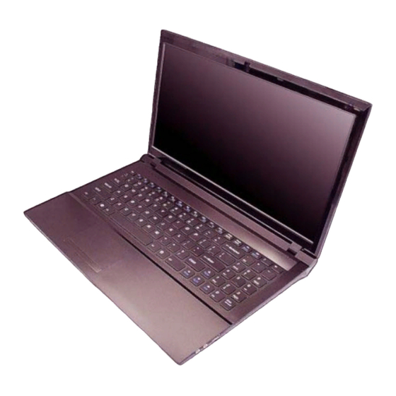
Page 17: External Locator - Top View With Lcd Panel Open
Introduction External Locator - Top View with LCD Panel Open Figure 1 Top View 1. PC Camera (Optional) 2. LCD 3. Power Button 4. LED Status Indicators 5. Keyboard 6. Built-In Microphone *Note that the microphone location is dependent upon your model design 7. -
Page 18: External Locator - Front & Right Side Views
Introduction External Locator - Front & Right Side Views Figure 2 Front View 1. LED Power Indicator FRONT VIEW Figure 3 Right Side View 1. Microphone-In RIGHT SIDE VIEW Jack 2. Headphone-Out Jack 3. USB 2.0 Port 4. Optical Device Drive Bay 5. -
Page 19: External Locator - Left Side & Rear View
Introduction External Locator - Left Side & Rear View Figure 4 Left Side View 1. DC-In Jack 2. External Monitor Port LEFT SIDE VIEW 3. RJ-45 LAN Jack 4. HDMI-Out Port 5. USB 3.0 Ports 6. Vent 7. Multi-in-1 Card Reader 8. -
Page 20: External Locator - Bottom View
Introduction External Locator - Bottom View Figure 6 Bottom View 1. Battery 2. Component Bay Cover 3. Vent 4. Hard Disk Bay Cover 5. Speakers Overheating To prevent your com- puter from overhea- ting, make sure no- thing blocks any vent while the computer is in use. -
Page 21: Mainboard Overview - Top (Key Parts)
Introduction Mainboard Overview - Top (Key Parts) Figure 7 Mainboard Top Key Parts 1. KBC-ITE IT8518 2. VIA VT1802P 3. Realtek RTL8411 Mainboard Overview - Top (Key Parts) 1 - 9... -
Page 22: Mainboard Overview - Bottom (Key Parts)
Introduction Mainboard Overview - Bottom (Key Parts) Figure 8 Mainboard Bottom Key Parts 1. Memory Slots DDR3 SO-DIMM 2. CMOS Battery 3. Mini-Card Connector (WLAN Module) 4. CPU Socket (no CPU installed) 5. Mini-Card Connector (3G Module) 6. nVIDIA VGA 7. -
Page 23: Mainboard Overview - Top (Connectors)
Introduction Mainboard Overview - Top (Connectors) Figure 9 Mainboard Top Connectors 1. HDMI-Out Port 2. USB Port 3.0 3. eSATA Port 4. Speaker Cable Connector 5. Microphone Cable Connector 6. Audio Board Connector 7. TouchPad Cable Connector 1 8. TouchPad Cable Connector 2 9. -
Page 24: Mainboard Overview - Bottom (Connectors)
Introduction Mainboard Overview - Bottom (Connectors) Figure 10 Mainboard Bottom Connectors 1. ODD Connector 2. HDD Connector 3. CPU Fan Cable Connector 4. Multi-in-1 Card Reader 5. RJ-45 LAN Jack 6. External Monitor Port 7. DC-In Jack 8. CCD Cable Connector 9. -
Page 25: Disassembly
Chapter 2: Disassembly Overview This chapter provides step-by-step instructions for disassembling the W251ESQ/W255ES series notebook’s parts and subsystems. When it comes to reassembly, reverse the procedures (unless otherwise indicated). We suggest you completely review any procedure before you take the computer apart. -
Page 26: Maintenance Tools
Disassembly NOTE: All disassembly procedures assume that the system is turned OFF, and disconnected from any power supply (the battery is removed too). Maintenance Tools The following tools are recommended when working on the notebook PC: • M3 Philips-head screwdriver •... -
Page 27: Maintenance Precautions
Disassembly Maintenance Precautions The following precautions are a reminder. To avoid personal injury or damage to the computer while performing a re- moval and/or replacement job, take the following precautions: Power Safety Warning 1. Don't drop it. Perform your repairs and/or upgrades on a stable surface. If the computer falls, the case and other Before you undertake components could be damaged. -
Page 28: Disassembly Steps
Disassembly Disassembly Steps The following table lists the disassembly steps, and on which page to find the related information. PLEASE PERFORM THE DISASSEMBLY STEPS IN THE ORDER INDICATED. To remove the Battery: To remove the Keyboard: 1. Remove the battery page 2 - 5 1. -
Page 29: Removing The Battery
Disassembly Removing the Battery Figure 1 Battery Removal 1. Turn the computer off, and turn it over. 2. Slide the latch in the direction of the arrow (Figure 1a a. Slide the latch and hold it 3. Slide the latch in the direction of the arrow, and hold it in place (Figure 1a in place. -
Page 30: Removing The Hard Disk Drive
Disassembly Removing the Hard Disk Drive The hard disk drive can be taken out to accommodate other 2.5" serial (SATA) hard disk drives with a height of 9.5mm Figure 2 (h). Follow your operating system’s installation instructions, and install all necessary drivers and utilities (as outlined in HDD Assembly Chapter 4 of the User’s Manual) when setting up a new hard disk. - Page 31 Disassembly 3. Remove the hard disk bay cover (Figure 3b Figure 3 4. Grip the tab and slide the hard disk in the direction of arrow (Figure 3c HDD Assembly 5. Lift the hard disk assembly out of the bay (Figure 3d Removal (cont’d.) 6.
-
Page 32: Removing The Optical (Cd/Dvd) Device
Disassembly Removing the Optical (CD/DVD) Device Figure 4 Optical Device 1. Turn off the computer, remove the battery (page 2 - Removal 2. Locate the component bay cover and remove screws (Figure 4a 3. Carefully (a fan and cable are attached to the under side of the cover) lift up the bay cover. a. -
Page 33: Removing The System Memory (Ram)
Disassembly Removing the System Memory (RAM) Figure 5 RAM Module The computer has two memory sockets for 204 pin Small Outline Dual In-line Memory Modules (SO-DIMM) supporting Removal DDRIII (DDR3) Up to 1066/1333 MHz. The main memory can be expanded up to 8GB. The SO-DIMM modules sup- ported are 1024MB and 2048MB DDRIII Modules. - Page 34 Disassembly 6. Gently pull the two release latches ( & ) on the sides of the memory socket in the direction indicated by the Figure 6 arrows (Figure 6c). The RAM module will pop-up Figure 6d , and you can then remove it RAM Module 7.
-
Page 35: Removing And Installing A Processor
Disassembly Removing and Installing a Processor Figure 7 Processor Removal Processor Removal Procedure 1. Turn off the computer, turn it over, and remove the battery (page 2 - 5) and the component bay cover (page 2 - a. The CPU heat sink will 2. - Page 36 Disassembly 5. Turn the release latch towards the unlock symbol to release the CPU (Figure 8d). Figure 8 6. Carefully (it may be hot) lift the CPU up and out of the socket (Figure 8e). Processor Removal 7. Reverse the process to install a new CPU. (cont’d) 8.
-
Page 37: Processor Installation Procedure
Disassembly Processor Installation Procedure Figure 9 1. Insert the CPU (Figure 9a), pay careful attention to the pin alignment, it will fit only one way (DO NOT FORCE Processor Installation IT!), and turn the release latch towards the lock symbol (Figure 9b). -
Page 38: Removing The 3.75G Module
Disassembly Removing the 3.75G Module Figure 10 3G Module Removal 1. Turn off the computer, turn it over, and remove the battery (page 2 - 5) and the component bay cover (page 2 - 2. The 3.75G module will be visible at point on the mainboard (Figure 10a). -
Page 39: Removing The Wireless Lan Module
Disassembly Removing the Wireless LAN Module Figure 11 Wireless LAN 1. Turn off the computer, turn it over, and remove the battery (page 2 - 5) and the component bay cover (page 2 - Module Removal 2. The Wireless LAN module will be visible at point on the mainboard (Figure 11a). -
Page 40: Removing The Keyboard
Disassembly Removing the Keyboard Figure 12 Keyboard Removal 1. Turn off the computer, and remove the battery (page 2 - 2. Remove screws from the bottom of the computer. Press at points to unsnap the LED cover module a. Remove screws from the bottom of the computer. -
Page 41: Part Lists
Appendix A:Part Lists This appendix breaks down the W251ESQ/W255ES series notebook’s construction into a series of illustrations. The component part numbers are indicated in the tables opposite the drawings. Note: This section indicates the manufacturer’s part numbers. Your organization may use a different system, so be sure to cross-check any relevant documentation. -
Page 42: Part List Illustration Location
Part List Illustration Location The following table indicates where to find the appropriate part list illustration. Table A - 1 Part List Illustration Part W251ESQ W255ES Location page A - 3 page A - 4 page A - 5 Bottom... -
Page 43: Top (W251Esq
Top (W251ESQ) Figure A - 1 Top (W251ESQ) 非耐落 (灰色) (尚盟) Top (W251ESQ) A - 3... -
Page 44: Top (W255Es
Top (W255ES) Figure A - 2 Top (W255ES) 非耐落 (灰色) ( 尚 盟) A - 4 Top (W255ES) -
Page 45: Bottom
Bottom Figure A - 3 Bottom Bottom A - 5... -
Page 46: Sata Blu Ray Combo
SATA BLU RAY COMBO Figure A - 4 SATA BLU RAY COMBO 非耐落 志精 A - 6 SATA BLU RAY COMBO... -
Page 47: Dvd Dual
DVD DUAL Figure A - 5 DVD DUAL 非耐落 志精 DVD DUAL A - 7... -
Page 48: Lcd
Figure A - 6 頭厚 非耐落 中性 A - 8 LCD... - Page 49 LCD A - 9...
- Page 50 A - 10...
-
Page 51: Schematic Diagrams
Schematic Diagrams Appendix B: Schematic Diagrams This appendix has circuit diagrams of the W251ESQ/W255ES notebook’s PCB’s. The following table indicates where to find the appropriate schematic diagram. Diagram - Page Diagram - Page Diagram - Page Table B - 1... -
Page 52: Schematic Diagrams
Schematic Diagrams System Block Diagram W25x/27x ESQ,EPQ VDD3,VDD5 Nvidia W251HPQ 6IN1 6-7P-W25P6-001 Fermi N13M GE1 Chief River System Block Diagram W251HPQ MAIN BOARD RAM SIZE: 1GB GPU NVDIDA NVVDD 6-71-W25P0-D02 (128Mx16x4pcs) AUDIO BOARD 5V,3V,5VS,3VS,1.5VS, PCIE*8 PHONE JACK x2, USB x1 6-71-W25P8-D02 Ivy Bridge 1.8VS,+1.5S_CPU... -
Page 53: Processor 1/7-Dmi, Fdi, Peg
Schematic Diagrams Processor 1/7-DMI, FDI, PEG Ivy Bridge Processor 1/7 ( DMI,PEG,FDI ) 1.05VS_VTT Ivy Bridge Quad Core 55W U36A 20 mil PEG_IR COMP_R R140 24.9_1%_04 PEG_ICOMPI Ivy Bridge Dual Core 35W PEG_ICOMPO H 22 DMI_TXN0 DMI_RX#[0] PEG_RCOMPO DMI_TXN1 DMI_RX#[1] Ivy Bridge LV/ULV 25/17W DMI_TXN2 DMI_RX#[2]... -
Page 54: Processor 2/7-Clk, Misc
Schematic Diagrams Processor 2/7 - CLK, MISC Ivy Bridge Processor 2/7 ( CLK,MISC,JTAG ) Processor Pullups/Pull downs PU/PD for JTAG signals 1.05VS_VTT 1.05VS_VTT H_PROCHOT# R115 62_04 R498 51_04 XDP_TMS R494 51_04 XDP_TDI_R CAD Note: Use pad sharing method XDP_PREQ# H_CPUPWRGD_R R496 *51_04 U36B... -
Page 55: Processor 3/7- (Ddr3
Schematic Diagrams Processor 3/7- (DDR3) Ivy Bridge Processor 3/7 ( DDR3 ) U36C U36D M_A_DQ[63:0] M_A_CLK_DDR0 9 M_B_DQ[63:0] M_B_CLK_DDR2 10 SA_CK[0] SB_CK[0] M_A_CLK_DDR#0 9 M_B_CLK_DDR#2 10 SA_CLK#[0] SB_CLK#[0] M_A_DQ0 M_B_DQ0 M_A_CKE0 9 M_B_CKE2 10 SA_DQ[0] SA_CKE[0] SB_DQ[0] SB_CKE[0] M_A_DQ1 M_B_DQ1 SA_DQ[1] SB_DQ[1] M_A_DQ2... -
Page 56: Processor 4/7- Power
Schematic Diagrams Processor 4/7- Power Ivy Bridge Processor 4/7 ( POWER ) VCORE PROCESSOR CORE POWER POWER U36F 22u_6.3V_X5R_08 * 10Pcs VCORE PROCESSOR UNCORE POWER 10u_6.3V_X5R_06 * 6Pcs 8.5A 1.05VS_VTT 1.05VS_VTT 560u_2.5V_6.6*6.6*5.9 * 4Pcs 8.5A AG35 AG34 VCC1 AH13 VCC2 VCCIO1 AG33 AH10... -
Page 57: Processor 5/7- Gfx Pwr
Schematic Diagrams Processor 5/7- GFX PWR Ivy Bridge Processor 5/7 ( GRAPHICS POWER ) 1.5VS_CPU POWER U36G R210 VGFX_CORE 1K_1%_04 AT24 AK35 *AO3402L VR1_VCCGT_SENSEA 40 VAXG1 VAXG_SENSE AT23 AK34 V_SM_VREF V_SM_VREF_CNT VR1_VSSGT_SENSEA 40 AT21 VAXG2 VSSAXG_SENSE C242 C215 C241 C633 C243 VAXG3 AT20... -
Page 58: Processor 6/7- Gnd
Schematic Diagrams Processor 6/7- GND Ivy Bridge Processor 6/7 ( GND ) U36H U36I AT35 AJ22 VSS1 VSS81 AT32 AJ19 VSS2 VSS82 AT29 AJ16 VSS3 VSS83 VSS161 VSS234 AT27 AJ13 AT25 VSS4 VSS84 AJ10 VSS162 VSS235 VSS5 VSS85 VSS163 VSS236 AT22 VSS6 VSS86... -
Page 59: Processor 7/7- Rsvd
Schematic Diagrams Processor 7/7- RSVD Ivy Bridge Processor 7/7 ( RESERVED ) CFG Straps for Processor PEG Static Lane Reversal - CFG2 is for the 16x 1:(Default) Normal Operation; Lane # CFG2 definition matches socket pin map definition U36E 0:Lane Reversed AH27 R132 0_04... -
Page 60: Ddr3 So-Dimm_0
Schematic Diagrams DDR3 SO-DIMM_0 SO-DIMM A C399 *10p_50V_NPO_04 M_A_CLK_DDR 0 M_A_CLK_D DR#0 JD IMM2A M_A_A[15:0] M_A_DQ[63:0] 4 M_A_A0 M_A_DQ0 C397 *10p_50V_NPO_04 JDIMM2B M_A_CLK_DDR 1 M_A_CLK_D DR#1 M_A_A1 M_A_DQ1 M_A_A2 M_A_DQ2 1.5V M_A_A3 M_A_DQ3 M_A_A4 M_A_DQ4 M_A_A5 M_A_DQ5 VD D1 VSS16 M_A_A6 M_A_DQ6 VD D2... -
Page 61: Ddr3 So-Dimm_1
Schematic Diagrams DDR3 SO-DIMM_1 SO-DIMM B J DIMM1B C 360 *10p_50V_N PO_04 M_B_CLK_DD R2 M_B_C LK_D DR #2 1. 5V JDIMM1A M_B_A[15:0] M_B_D Q[ 63:0] 4 M_B_A0 M_B_D Q0 C 353 *10p_50V_N PO_04 D Q0 M_B_CLK_DD R3 M_B_C LK_D DR #3 M_B_A1 M_B_D Q1 D Q1... -
Page 62: Panel, Inverter, Crt
Schematic Diagrams PANEL, INVERTER, CRT PANEL CONNECTOR (30Pin & 40Pin CO-lay) PANEL POWER 3.3VS 2.2K_04 PLVDD 2.2K_04 VDD3 SY S15V VIN_LCD MTN2604G6 For Safety LPS. 3.3VS J_LCD1 P_DDC_DATA 0.2_06 0.2_06 P_DDC_CLK R440 0.2_06 0.2_06 BRIGHTNESS_R 1M_04 1M_04 INV_BLON 0.1u_50V_Y5V_06 0.1u_50V_Y5V_06 LVDS-LCLKN LVDS-L2N DTC114EUA... -
Page 63: Vga Pci-E Interface
Schematic Diagrams VGA PCI-E Interface 3. 3VS C299 N13P-GL N13M-GE1 Strap U 10 1u_6.3V_X5R_04 MC74VHC1G08DFT2G VGA_ROM_SI 20K / Low 45.3K / Low 22,34 dGPU_RST# PERSTB# 3V3_RUN 3,22,28 PLT_RST# R192 VGA_ROM_SO 30K / Low 30K / Low 100K_04 3V3_RUN VGA_ROM_SCLK 15K / Low 15K / High 10K_04 R191... -
Page 64: Vga Frame Buffer Interface
Schematic Diagrams VGA Frame Buffer Interface Frame Buffer Interface U32C FBC_CMD[31:0] FBC_CMD[31:0] 15 U32B 3/19 FBB 2/19 FBA FBC_D[63: 0] FBA_D[63:0] FBC_D[63:0] FBA_D[63:0] FBC_D0 FBB_D0 FBA_D0 R625 *0_04 FBC_D1 FBA_D0 FB_CLAMP FBB_D1 FBA_D1 FBC_D2 FBA_D1 FBB_D2 FBA_D2 FBC_D3 FBA_D2 C100819 FBB_D3 FBA_D3 FBC_D4... -
Page 65: Vga Frame Buffer A
Schematic Diagrams VGA Frame Buffer A Frame Buffer Partition A FBVDDQ C607 C644 C577 C653 C649 C240 C233 C650 C596 C 600 C648 C645 1u_6.3V_X5R_04 1u_6.3V_X5R_04 1u_6.3V_X5R_04 1u_6.3V_X5R_04 1u_6.3V_X5R_04 1u_6.3V_X5R_04 1u_6.3V_X5R_04 1u_6.3V_X5R_04 1u_6.3V_X5R_04 1u_6.3V_X5R_04 1u_6.3V_X5R_04 1u_6. 3V_X5R_04 0.1uF X4 for FBVDDQ one chip VRAM 1.0uF X8 FBVD DQ FBVDDQ... -
Page 66: Vga Frame Buffer C
Schematic Diagrams VGA Frame Buffer C Frame Buffer Partition B FBVDDQ C657 C611 C613 C608 C595 C 609 C614 C285 C576 C103 1u_6.3V_X5R_04 1u_6.3V_X5R_04 1u_6.3V_X5R_04 1u_6.3V_X5R_04 1u_6.3V_X5R_04 1u_6.3V_X5R_04 1u_6.3V_X5R_04 1u_6.3V_X5R_04 1u_6. 3V_X5R_04 1u_6.3V_X5R_04 1u_6.3V_X5R_04 1u_6.3V_X5R_04 FBVDDQ FBVDDQ FBC_CMD[31:0] FBC_CMD[31:0] C574 C583 C582 C581... -
Page 67: Vga I/O
Schematic Diagrams VGA I/O U32M 9/19 IFPEF U32K U32L 7/19 IFPC 8/19 IFPD ALL PINS NC FOR GF117 ALL PINS NC FOR GF117 ALL PINS NC FOR GF117 DVI-DL DVI-SL/HDMI IFPC_RSET IFPD_RSET DVI/HDMI DVI/HDMI IFPE_AUX RN13 I2CY_SDA I2CY_SDA I2CY_SCL I2CY_SCL IFPE_AUX IFPC_PLLVDD IFPD_PLLVDD... -
Page 68: Vga Nvvdd Cecoupling
Schematic Diagrams VGA NVVDD Cecoupling NVVDD NVVDD U32G U32I U32E U32H 10/19 XVDD 16/19 GND_1/2 14/19 NVVDD 17/19 GND_2/2 AM25 AA17 AA12 CONFIGURABLE AA18 AN10 AA14 POWER AA20 AN13 AA16 C130 C128 C127 CHANNELS AA22 AN16 AA19 XVDD AB12 AN19 AA21 0.1u_10V_X5R_04 0.1u_10V_X5R_04... -
Page 69: Pch 1/9- Rtc, Hda, Sata
Schematic Diagrams PCH 1/9- RTC, HDA, SATA NO REBOOT STRAP PantherPoint - M (HDA,JTAG,SATA) NO REBOOT STRAP: HDA_SPKR High Enable 3.3VS 20mils RTCVCC BAT54CS3 20mils VDD3 HDA_SPKR R271 *1K_04 C446 1u_6.3V_X5R_04 RTC_VBAT_1 C100810 C712 R315 12p_50V_NPO_04 iTPM ENABLE/DISABLE del X9 ¨ú®ø32.768 CO-LAY C101004 20K_1%_04 TPM FUNCTION:SPI_SI High Enable R313... -
Page 70: Pch 2/9- Pcie, Smbus, Clk
Schematic Diagrams PCH 2/9- PCIE, SMBUS, CLK 3.3V 2.2K_8P4R_04 PantherPoint - M (PCI-E,SMBUS,CLK) SMB_CLK SMB_DATA SML0_CLK SML0_DATA U39B 10K_8P4R_04 BG34 BT_SBD# PERN1 BJ34 BT_SBD# LPD_SPI_INTR# BT_SBD# 27 PERP1 SMBALERT# / GPIO11 AV32 PEG_PCIECLKRQ7# PETN1 AU32 SMB_CLK PEG_B_CLKRQ# SMB_CLK 9,10 PETP1 SMBCLK BE34 SMB_DATA... -
Page 71: Pch 3/9- Dmi, Fdi, Pwrgd
Schematic Diagrams PCH 3/9- DMI, FDI, PWRGD PantherPoint -M (DMI,FDI,GPIO) U39C 3.3V BC24 BJ14 FDI_TXN0 2 DMI_RXN0 DMI0RXN FDI_RXN0 BE20 AY 14 FDI_TXN1 2 DMI_RXN1 DMI1RXN FDI_RXN1 BG18 BE14 AC_PRESENT R302 10K_04 FDI_TXN2 2 DMI_RXN2 BG20 DMI2RXN FDI_RXN2 BH13 PM_SLP_LAN# R283 *10K_04 DMI_RXN3... -
Page 72: Pch 4/9- Lvds, Ddi, Crt
Schematic Diagrams PCH 4/9- LVDS, DDI, CRT PantherPoint -M (LVDS,DDI) U39D AP43 BLON L_BKLTEN SD VO_TVCLKIN N AP45 11,34 NB_EN AVDD L_VD D_EN SDVO_TVC LKINP AM42 L_BKLTCTL SDVO_STALLN AM40 SDVO_STALLP Sheet 21 of 50 Ver:1.0 P_DDC _CLK L_D DC _C LK AP39 3.3VS pull up 2.2K... -
Page 73: Pch 4/9- Pci, Usb, Rsvd
Schematic Diagrams PCH 4/9- PCI, USB, RSVD PantherPoint -M (PCI,USB,NVRAM) 3.3V 10K_8P4R _04 USB_OC#23 U39E USB_OC#89 Boot BIOS Strap AY 7 USB_OC#1213 RSVD1 RSVD2 BG26 BBS_BIT1 BBS_BIT0 Boot BIOS Location RN17 RSVD3 BJ26 10K_8P4R _04 RSVD4 BH 25 USB_OC#14 BJ16 AT10 USB_OC#67 BG16... -
Page 74: Pch 6/9- Gpio, Cpu
Schematic Diagrams PCH 6/9- GPIO, CPU PantherPoint - M (GPIO,VSS_NCTF,RSVD) 3.3V R552 1K_04 HOST_ALERT#1 R264 1K_04 HOST_ALERT#2 3.3VS LED_DGPU# R251 *10K_04 U39F DGPU_PWROK R390 *10K_04 SATA_ODD_PWRGT S_GPIO SATA_ODD_PWRGT R361 1K_04 BMBUSY# / GPIO0 TACH4 / GPIO68 SATA_ODD_PWRGT 31 R548 10K_04 MFG_MODE R558 10K_04... -
Page 75: Pch 7/9- Pwr
Schematic Diagrams PCH 7/9- PWR 1.05VS PantherPoint -M (POWER) 1u_6.3V_X5R_04 * 3Pcs 3.3VS HCB1608KF-121T25 CLOSE TO CHIP C100823 10u_6.3V_X5R_06 * 1Pcs POWER U39G 1.05VS VCCA_DAC_3.3VS 1.3A AA23 VCCA_DAC3.3VS 0_06 VCCCORE[1] VCCADAC AC23 VCCCORE[2] C458 C464 C451 C448 AD21 C754 C735 C736 C741 C523... -
Page 76: Pch 8/9 Power
Schematic Diagrams PCH 8/9 POWER PantherPoint - M (POWER) CougarPoint power supply range 1.05VS_VCCA_CLK *HCB1005KF-121T20 1.05VS Voltage 1.05VS POWER U39J 2.92A 1.00V 1.05V 1.10V 3.3V AD49 C426 Note: For CPT/PPT Default 1.43V 1.5V 1.58V VCCACLK VCCIO[29] C453 mode:Internal VR C449,C476 0.1u_10V_X5R_04 1.71V 1.8V... -
Page 77: Pch 9/9- Gnd
Schematic Diagrams PCH 9/9- GND PantherPoint -M (GND) Voltage Rail Voltage S0 Iccmax Current (A) U39I V_CPU_IO 1.05 1 (mA) U39H AY 4 V5REF 1 (mA) VSS[159] VSS[259] VSS[0] AY42 AY46 VSS[160] VSS[260] AA17 AK38 V5REF_Sus 1 (mA) VSS[161] VSS[261] VSS[1] VSS[80] AY 8... -
Page 78: Wlan, 3G, Mini Pcie
Schematic Diagrams WLAN, 3G, MINI PCIE 3G/MSATA MINI CARD C588 220u_6.3V_6.3*6.3*4.2 J_SIM1 SIM CONN C177 0.1u_16V_Y 5V_04 (TOP VIEW) *10mil_short_04 DETECT_SW UIM_MCMD J_3G1 UIM_PWR *4.7K_04 UIM_DATA UIM_D UIM_DATA 60mils UIM_DATA UIM_I/O UIM_CLK UIM_C UIM_VPP WAKE# 3.3VAUX_0 3G_3.3V UIM_CLK UIM_VPP UIM_RST *10mil_short_04 COEX1 1.5V_0... -
Page 79: Ccd, Tpm, Multi Con
Schematic Diagrams CCD, TPM, MULTI CON FOR POWER SW BOARD FOR OPTIMUS FUNCTION CPU FAN CONTROL FON# 3.3VS 3.3V 5VS_FAN VOUT C326 VSET J_SW1 1u_10V_Y 5V_06 AX995SA 04->06 C100824 20mil CPU_FAN 34 MBTN *10mil_short_04 AX995B(SOT23-6) & APE8872 6-02-03940-B20 M_BTN# WEB_WWW# C350 6-02-00995-B20 Co-Layout... -
Page 80: Usb3.0
Schematic Diagrams USB3.0 3.3V_USB3 1.1V HCB1608KF-121T25 C290 C297 C308 C287 C306 C263 C266 C267 C289 C270 C277 C276 C309 C262 C313 C268 C307 C269 C314 C282 C302 0.1u_16V_Y 5V_04 0.1u_16V_Y 5V_04 0.1u_16V_Y 5V_04 0.01u_16V_X7R_04 0.01u_16V_X7R_04 0.01u_16V_X7R_04 0.1u_16V_Y 5V_04 0.1u_16V_Y 5V_04 0.1u_16V_Y 5V_04 0.1u_16V_Y 5V_04 0.01u_16V_X7R_04... -
Page 81: Card Reader (Rtl8411
Schematic Diagrams Card Reader (RTL8411) Switching Regulator close to pin48 RTL8411 LAN_VDD33 VDD33/18 R307 0_06 VDD10 (Shape) (Shape) VDD10 *SWF2520CF-4R7M-M LAN_VDD33 REGLX VDD10 mode mode C522 C521 *4.7u_6.3V_X5R_06 *0.1u_16V_Y 5V_04 REGLX VDD3 VDD3 REGLX and VDD10 must be shape R406 R407 R419 L37¡BC177¡BC448 must close to Pin 48... -
Page 82: Sata Odd, Led, Usb Charge
Schematic Diagrams SATA ODD, LED, USB CHARGE Switching Regulator close to pin48 RTL8411 LAN_VDD33 VDD33/18 R307 0_06 VDD10 (Shape) (Shape) VDD10 *SWF2520CF-4R7M-M LAN_VDD33 REGLX VDD10 mode mode C522 C521 *4.7u_6.3V_X5R_06 *0.1u_16V_Y 5V_04 REGLX VDD3 VDD3 REGLX and VDD10 must be shape R406 R407 R419... -
Page 83: Hdmi, Rj45
Schematic Diagrams HDMI, RJ45 FOR W/O LEVEL SHIFT GIGA LAN (JMC251C) LAN PORT LAN_MDIN0 LMX1- LAN_MDIN0 TD4- MX4- LAN_MDIP0 LMX1+ 0_8P4R_04 LAN_MDIP0 TD4+ MX4+ LAN_MDIN1 LMX2- HDMIC_C0CP_C TMDS_DATA2-L LAN_MDIN1 TD3- MX3- LAN_MDIP1 LMX2+ HDMIC_C0CN_C TMDS_DATA2#-L LAN_MDIP1 TD3+ MX3+ 3.3VS HDMIC_C1CP_C TMDS_DATA1-L VDD10 HDMIC_C1CN_C... -
Page 84: Audio Codec Vt1802P
Schematic Diagrams AUDIO CODEC VT1802P CODEC (ALC269 & VT1802P) PVDD1_2 R338 Layout note: *15mil_short_06 EMI Require R401 *0_06 GND and AUDG space is 1.5V 60mils ~ 100mils For 1.5V HDA Link. DVDD_IO C486 C483 *HCB1005KF-121T20 20 mil R378 0_06 0.1u_16V_Y 5V_04 10u_6.3V_X5R_06 3.3VS_AUD *10mil_short_04... -
Page 85: Kbc-Ite It8518E
Schematic Diagrams KBC-ITE IT8518E KBC_AVDD HCB1005KF-121T20 VDD3 VDD3 VDD3 C436 C510 C502 C487 C544 C416 C437 C415 0.1u_16V_Y 5V_04 10u_6.3V_X5R_06 0.1u_16V_Y5V_04 0.1u_16V_Y 5V_04 0.1u_16V_Y 5V_04 *0.1u_16V_Y 5V_04 *0.1u_16V_Y 5V_04 R416 J_KB1 C541 100K_04 HCB1005KF-121T20 0.1u_16V_Y5V_04 KBC_AGND FOR W250HPQ FOR W270HU EC_VCC KBC_WRESET# 3.3VS... -
Page 86: 5Vs, 3Vs, 1.5Vs Cpu
Schematic Diagrams 5VS, 3VS, 1.5VS CPU VIN1 PR114 100K_04 DD_ON VIN1 DDON_LATCH PR115 *100K_04 DD_ON_LATCH USB_CHARGE_EN 34,36 PWR_SW #_R PR130 1K_04 PR116 10K_04 VDD3 M_BTN# M_BTN# PW R_SW# USB_CHARGE_EN R622 1K_04 PR117 1K_04 INSTANT-ON PWR_SW# 34 R623 100K_04 P2808B0 for ¦@¥ÎR3_4_8_12 C100820 for ¦@¥ÎR3_4_8_12 C100816 ¹w¯dPJ17¡Acost down 5V MOS W USB Charge ¤W¥ó... -
Page 87: Vdd3, Vdd5
Schematic Diagrams VDD3, VDD5 VREF_VDD PR126 *0_04 PR127 *20mil_04 PC49 1u_10V_Y 5V_06 VFB2 VFB1 PR132 PR129 EN_3V EN_5V PC55 100K_04 100K_04 PC56 1000p_50V_X7R_04 1000p_50V_X7R_04 VREG3 PC206 PC205 PC54 PR133 *10K_04 4.7u_25V_X5R_08 4.7u_25V_X5R_08 5608POK PC70 PC71 SY S5V VDD3 LDO3 VDD5 1u_10V_Y 5V_06 PC209 PC204... -
Page 88: Power 0.85Vs, 1.8Vs
Schematic Diagrams Power 0.85VS, 1.8VS -n²¾¾aªñPIN6¸} 1.8VS 3.3 V PC40 V1.8 2.2u_6.3V_Y5V_06 1.8VS PR108 10K_04 3.3V VCNTL 1.8VS_PWRGD R217 *10mil_short_04 POK_6610 3,20 1.8VS_PWRGD VOUT *OPEN-3mm VOUT PR110 10K_04 EN1.8VS1 PC44 PC39 PC45 VFB_6610 PC42 PR113 1.3K_1%_04 PQ19 *1u_6.3V_Y5V_04 2SK3018S3 PR109 1M_04 EN1.8VS AX6615ESA... -
Page 89: Power 1.5V/1.05Vs
Schematic Diagrams POWER 1.5V/1.05VS PD18 PC220 PC76 PC75 PC215 PQ64 RB0540S2 ME4894-G PU10 VDDQ VTT_MEM PC223 1.5V 10u_6.3V_X5R_06 VBST PC77 0.1u_10V_X7R_04 VLDOIN VBST VDDQ PJ30 PL10 PR266 DRVH TMPC 1004H-1R0M-Z01 PJ15 VTT_MEM DR VH 3.3_06 1.5V *OPEN-2mm PR149 PC214 *OPEN-8mm PC224 PC222 PC221... -
Page 90: Power 1.05V/1.05Vs Vtt
Schematic Diagrams POWER 1.05V/1.05VS VTT SYS15V V1.05 PQ74 1.05VS_VTT *ME4626-G PR288 3.3V *1M_04 PR289 *100K_04 PQ75 R648 C769 *2N7002W *10K_04 *2200p_50V_X7R_04 1.05VS_VTT_EN# Sheet 39 of 50 1.05VS_VTT_EN *MTN7002ZHS3 POWER 1.05VS/ C100824 1.05VS VTT 1.05VS_VTT PJ34 *8mm PQ55 *ME4626-G 1.05VS_VTT V1.05 PC192 PC189 4.7u_25V_X5R_08... -
Page 91: Power Vcore1
Schematic Diagrams POWER VCORE1 PR236 PC180 * 1K_1%_04 * 100p_X7R_04 PR243 0_04 PC179 1000p_50V_X7R_04 PC172 0.1u_10V_X7R_04 PUT COLSE PR238 24K_1%_04 TO GT CSCOMPA DROOPA CSREFA PR246 Inductor 165K_1%_04 PR237 1.6K_1%_04 PR242 * 4.7K_1%_04 PR239 PC181 PC173 10p_50V_N PO_04 1.05VS_VTT PUT COLSE TO CPU 10_1%_04 33p_50V_NPO_04... -
Page 92: Power Vcore2
Schematic Diagrams POWER VCORE2 PC122 PC110 PC111 PC109 PC116 PC107 PC106 PC108 PQ40 PQ41 PQ43 PQ42 NTMFS4926N NTMFS4926N NTMFS4926N NTMFS4926N Sheet 41 of 50 DCR 1.1mohm DCR 1.1mohm SW 1 SW 1 VCORE VCORE 0.36UH_12.9* 14*3.8 0.36UH_12. 9*14*3. 8 POWER VCORE2 PQ10 PQ47 PQ49... -
Page 93: Power Vga Nvvdd/Pex_Vdd
Schematic Diagrams Power VGA NVVDD/PEX_VDD 3V3_RUN NM OS VGA__NVVDD SY S15V 3.3V MTN2604G6 3V3_RUN 1M_04 PR163 4.7u_6.3V_X5R_06 100_04 dGPU_PWR_EN *1n_50V_04 NCPEN C100809 SGND2 PR171 PQ35B *10mil_short ADP3212_CSREF 2200p_50V_X7R_04 PR167 PQ35A MTDK5S6R *47K_04 MTDK5S6R dGPU_PWR_EN# 22,34 CS_PH1 PR164 215K_1%_06 PJ32 CS_PH2 PR13 215K_1%_06 PR15 20K_1%_04... -
Page 94: Ac In, Charger
Schematic Diagrams AC IN, CHARGER PR178 *20mil_04 PR179 *470K_04 PQ39 V_BAT MEP4435Q8 J_DC_JACK1 ¾aªñJBATTA1 50932-00301-001 PQ34 8.2UH_7.3*6.6*2.8MM HCB4532K-800_18 MEP4435Q8 PQ45A PC80 PR165 PD1503YVS PQ45B PR181 0.01_1%_32 PD1503Y VS TMPB0603M-8R2MN-Z01 0.01_1%_32 GND1 GND2 PR160 10K_04 PR185 *5.1_06 100K_04 PC19 PC126 PC18 *220p_50V_NPO_04 0.047u_10V_X7R_04 0.047u_10V_X7R_04... -
Page 95: Audio Board
Schematic Diagrams AUDIO BOARD USB PORT A_USBVCC A_USBVCC2 HCB1608KF-121T25 60 mil 100u_6.3V_B_A 0.1u_16V_Y5V_04 AJ_USB1 Port1 AGND AUSB_PN1 AUSB_PN1_R DATA_L AUSB_PP1 AUSB_PP1_R DATA_H *WCM2012F2S-SHORT D02A US04036BCA081 Change footprint 6-21-B49C0-104 6-21-B49B0-104 AGND TO M/B AUDIO JACK Sheet 44 of 50 AUDIO BOARD AJ_MIC1 AMIC_SENSE AMIC1-R... -
Page 96: Click Board
Schematic Diagrams CLICK BOARD CLICK BOARD CLED_PWR CLED_BAT_FULL CLED_ACIN CLED_BAT_CHG CR360 CR359 CR361 CR358 220_04 220_04 220_04 0.1u_16V_Y 5V_04 *0.1u_16V_Y5V_04 *0.1u_16V_Y 5V_04 220_04 POWER ON C5VS C5VS CVDD3 BAT LED CD27 CD26 CGND CGND CGND CJ_TP2 CJ_TP3 CJ_TP1 RY -SP155HY YG4-1 RY -SP155HY Y G4-1 CTP_DATA CTP_CLK... -
Page 97: W251Hpq Power Sw Board
Schematic Diagrams W251HPQ POWER SW BOARD S_3.3VS POWER POWER SW & LED SWITCH S_3.3V LID SWITCH IC 220_04 *BAV99 RECTIFIER S_3.3V 20mil 20mil Z4301 S_3.3VS S_3.3V 100K_04 SLID _SW# SJ_SW2 0.1u_16V_Y 5V_04 20mil SM_BTN# *H T-150NB-DT SMGND SWEB_WWW# HT-150NB-DT MH 248-ALFA-ESO SWEB_EMAIL# 0.1u_16V_Y 5V_04 *100p_50V_NPO_04... -
Page 98: W270Hu Bridge Odd Board
Schematic Diagrams W270HU BRIDGE ODD BOARD ODD BOARD FOR W270HU M/B ºÝ ODD board ºÝ QJ_ODD1 QJ_ODD2 Sheet 47 of 50 Q_SATA_TXP1 Q_SATA_TXN 1 W270HU BRIDGE Q_SATA_RXN1 Q_SATA_RXP1 ODD BOARD QGND QGND Q_ODD_DETECT# Q_5VS Q_5VS Q_SATA_ODD_DA# 242001-1 202001-1 P IN P IN QGND QGND... -
Page 99: W270Hu Power Sw Board
Schematic Diagrams W270HU POWER SW BOARD POWER SW & LED POWER SWITCH W_3.3VS W _3.3VS W_3.3V LID SWITCH IC W C1 *BAV99 RECTIF IER W _3.3V 0.1u_16V_Y 5V_04 W R2 WR 3 100K_04 220_04 220_04 220_04 220_04 WMGND WLID_SW# 20mil 20mil 20mil 20mil... -
Page 100: Power Diagram
Schematic Diagrams Power Diagram 3.3V 1.05VS PWR SW B'd 2.92A RTCVCC 3.3VS M_BTN# VCORE 1.05VS_VTT 1.5VS 1.05VS_VTT Cougar 8.5A 3.3VS VDD3 Point VGFX_CORE 1.5V ALL_SYS_PWRGD RSMRST# SO-DIMM 1.8VS RSMRST#, PMSYS_PWRGD_BUF 1.2A PWR_SW# DRAMPWROK DPWROK SM_DRAMPWROK IT8518 PWR_BTN# 1.5VS_CPU P2808B PWRBTN# H_CPUPWRGD PM_PCH_PWROK PWOCPWRGD... -
Page 101: Power On Seq
Schematic Diagrams Power On SEQ PWR_SW# 308ms PWR_SW# (PU6.6) DD_ON 84ms DD_ON (PQ27.2) 1.3ms 3.3V rise time=960us 3.3V 3.3V (PU4.5) (PQ64.1) 2.12ms 5V rise time=1.7ms (U14.3) (PQ66.1) RSMRST# 91.6ms RSMRST# (U17.35) PWR_BTN# 173ms 123ms PWR_BTN# (U17.33) SUSC# 204ms SUSC# (PQ11.5) 1.5V (PJ9) (C644.1) - Page 102 Schematic Diagrams B - 52...
-
Page 103: Updating The Flash Rom Bios
Download the BIOS computer model. 1. Go to www.clevo.com.tw and point to E-Services and click E-Channel. Note that BIOS versions 2. Use your user ID and password to access the appropriate download area (BIOS), and download the latest BIOS files... -
Page 104: Use The Flash Tools To Update The Bios
BIOS Update Use the flash tools to update the BIOS 1. Make sure you are not loading any memory management programs such as HIMEM by holding the F8 key as you see the message “Starting MS-DOS”. You will then be prompted to give “Y” or “N” responses to the programs being loaded by DOS.
Need help?
Do you have a question about the W251ESQ and is the answer not in the manual?
Questions and answers