Sign In
Upload
Download
Table of Contents
Contents
Add to my manuals
Delete from my manuals
Share
URL of this page:
HTML Link:
Bookmark this page
Add
Manual will be automatically added to "My Manuals"
Print this page
×
Bookmark added
×
Added to my manuals
Manuals
Brands
Clevo Manuals
Laptop
W251HPQ
Service manual
Clevo W251HPQ Service Manual
Hide thumbs
1
2
3
4
5
6
7
8
9
10
Table Of Contents
11
12
13
14
15
16
17
18
19
20
21
22
23
24
25
26
27
28
29
30
31
32
33
34
35
36
37
38
39
40
41
42
43
44
45
46
47
48
49
50
51
52
53
54
55
56
57
58
59
60
61
62
63
64
65
66
67
68
69
70
71
72
73
74
75
76
77
78
79
80
81
82
83
84
85
86
87
88
89
90
91
92
93
94
95
96
97
98
99
100
101
102
103
page
of
103
Go
/
103
Contents
Table of Contents
Bookmarks
Table of Contents
Instructions for Care and Operation
Power Safety
Battery Precautions
System Startup
Table of Contents
Introduction
Overview
Specifications
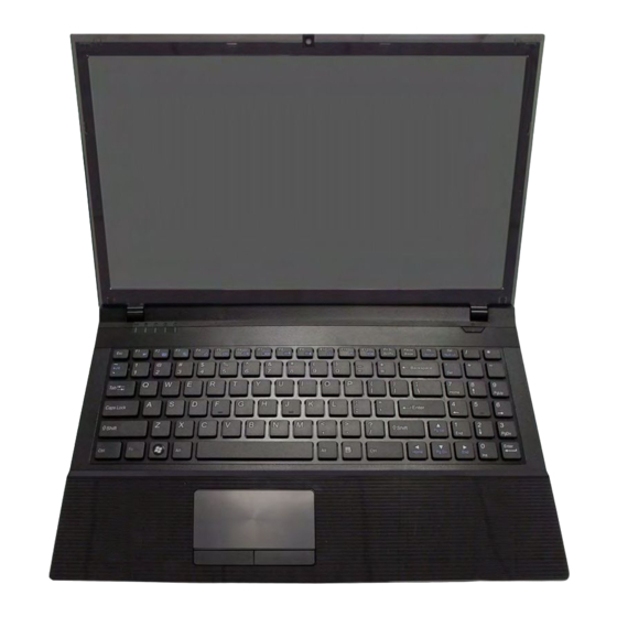
External Locator - Top View with LCD Panel Open
External Locator - Front & Right Side Views
External Locator - Left Side & Rear View
External Locator - Bottom View
Mainboard Overview - Top (Key Parts)
Mainboard Overview - Bottom (Key Parts)
Mainboard Overview - Top (Connectors)
Mainboard Overview - Bottom (Connectors)
Disassembly
Overview
Maintenance Tools
Connections
Maintenance Precautions
Disassembly Steps
Removing the Battery
Removing the Hard Disk Drive
Removing the Optical (CD/DVD) Device
Removing the System Memory (RAM)
Removing and Installing a Processor
Removing the 3.75G Module
Removing the Wireless LAN Module
Removing the Keyboard
Part Lists
Part List Illustration Location
Top (W251HPQ,W251HNQ
Top (W255HP,W255HN
Top (W258HPQ,W258HNQ
Bottom
Sata Blu Ray Combo
DVD Dual
Lcd
Schematic Diagrams
System Block Diagram
Processor 1/7-DMI, FDI, PEG
Processor 2/7- CLK, MISC
Processor 3/7- (DDR3
Processor 4/7- Power
Processor 5/7- GFX PWR
Processor 6/7- GND
Processor 7/7- RSVD
Ddr3 So-Dimm_0
Ddr3 So-Dimm_1
Panel, Inverter, Crt
VGA PCI-E Interace
VGA Frame Buffer Interface
VGA Frame Buffer a
VGA Frame Buffer C
Vga I/O
VGA NVVDD Cecoupling
Pch 1/9- Rtc, Hda, Sata
Pch 2/9- Pcie, Smbus, Clk
Pch 3/9- DMI, Fdi, Pwrgd
Pch 4/9- Lvds, DDI, Crt
Pch 4/9- Oci, Usb, Rsvd
Pch 6/9- Gpio, Cpu
Pch 7/9- Pwr
Pch 8/9 Power
Pch 3/9- Grd
Wlan 3G Mini Pcie
CCD, Tpm, Multi con
Usb2.0, Usb3.0 Nec
Card Reader (JMC251 C)
Sata Odd, Led, Usb Charge
Hdmi, Rj45
Audio Codec Alc269
Kbc-Ite It8518E
5Vs, 3Vs, 3.3Vm, 1.5Vs Cpu
Vdd3, Vdd5
Power 0.85VS, 1.8VS, PEX VDD
Power 1.5V/1.05Vs/0.75V
Power Vcore1
Power Vcore2
Power VGA NVVDD
Ac In, Charger
Audio Board
Click Board
W251Hpq Power Sw Board
W270Hu Bridge Odd Board
W270Hu Power Sw Board
Power Diagram
Power on SEQ
Updating the FLASH ROM BIOS
To Update the FLASH ROM BIOS You Must
Download the BIOS
Unzip the Downloaded Files to a Bootable CD/DVD/ or USB Flash Drive
Advertisement
Quick Links
1
Specifications
Download this manual
W251HPQ/W251HPQ-C/W251HNQ/W251HNQ-C/W255HP/W255HN/W258HPQ/W258HPQ-C/W258HNQ
Table of
Contents
Previous
Page
Next
Page
1
2
3
4
5
Advertisement
Table of Contents
Need help?
Do you have a question about the W251HPQ and is the answer not in the manual?
Ask a question
Questions and answers
Related Manuals for Clevo W251HPQ
Laptop Clevo W251EUQ Service Manual
(101 pages)
Laptop Clevo W251ESQ Service Manual
(104 pages)
Laptop Clevo W270EFQ User Manual
(346 pages)
Laptop Clevo 15CL44 Concise User Manual
(134 pages)
Laptop Clevo W255BU Service Manual
(93 pages)
Laptop Clevo W251BUQ User Manual
(83 pages)
Laptop Clevo W251BLQ Service Manual
(89 pages)
Laptop Clevo W250HU Service Manual
(97 pages)
Laptop Clevo W251HSQ Service Manual
(105 pages)
Laptop Clevo W251ELQ Service Manual
(101 pages)
Laptop Clevo W251CUQ-C Service Manual
(85 pages)
Laptop Clevo W255HP Service Manual
(103 pages)
Laptop Clevo W255EU Service Manual
(101 pages)
Laptop Clevo E5120Q Service Manual
(96 pages)
Laptop Clevo W25CSV series Service Manual
(103 pages)
Laptop Clevo W253EFQ Service Manual
(110 pages)
This manual is also suitable for:
W251hpq-c
W255hpq
W255hoq-c
W258hnq
W251hnq
W251nhq-c
...
Show all
W255hp
Table of Contents
Print
Rename the bookmark
Delete bookmark?
Delete from my manuals?
Login
Sign In
OR
Sign in with Facebook
Sign in with Google
Upload manual
Upload from disk
Upload from URL


Need help?
Do you have a question about the W251HPQ and is the answer not in the manual?
Questions and answers