Hytera PD70X Service Manual
Hide thumbs
Also See for PD70X:
- Service manual (513 pages) ,
- Owner's manual (27 pages) ,
- User manual (24 pages)
Table of Contents
Advertisement
Quick Links
Advertisement
Table of Contents
Troubleshooting

Subscribe to Our Youtube Channel
Related Manuals for Hytera PD70X


Summary of Contents for Hytera PD70X
- Page 1 SERVICE MANUAL DMR PORTABLE RADIO 数 字 手 持 对 讲 机...
- Page 2 This manual describes information related with product repair. To repair the product properly, please read this manual carefully. This manual is applicable to the following model: PD70X (X may indicate 2, 5, 6 or 8) PD70XG (X may indicate 2, 5, 6 or 8) PD78X (X may indicate 2, 5, 6 or 8)
-
Page 3: Table Of Contents
Service Manual Contents 1. Revision History ........................... 1 2. Copyright Information.......................... 2 3. Disclaimer ............................. 3 4. Introduction............................4 5. Product Controls ..........................5 6. Baseband Section ..........................7 6.1 Power Section ..........................7 6.2 Control Section..........................8 6.3 Audio Section ..........................14 6.4 Troubleshooting Flow Chart...................... - Page 4 Service Manual 11.2 Receiver Circuit ......................... 91 11.3 Frequency Generation Unit (FGU).................... 93 11.4 PCB View ..........................95 11.5 Block Diagram ......................... 103 11.6 Schematic Diagram......................... 106 11.7 Parts List..........................122 11.8 Troubleshooting Flow Chart ....................147 12. UHF3 (350-400MHz) Information....................154 12.1 Transmitter Circuit........................
-
Page 5: Revision History
Service Manual 1. Revision History Version Date Description R2.0 09-2010 Initial Release dd descriptions on VHF, UHF2 and UHF3; update the battery R3.5 05-2011 life. -
Page 6: Copyright Information
Service Manual 2. Copyright Information Hytera is the trademark or registered trademark of Hytera Communications Co., Ltd. (the Company) in PRC and/or other countries or areas. The Company retains the ownership of its trademarks and product names. All other trademarks and/or product names that may be used in this manual are properties of their respective owners. -
Page 7: Disclaimer
No part of this manual may be copied, modified, translated, or distributed in any manner without the express written permission of us. If you have any suggestions or would like to learn more details, please visit our website at: http://www.hytera.com. -
Page 8: Introduction
Service Manual 4. Introduction Intended User This manual is intended for use by qualified technicians only. -
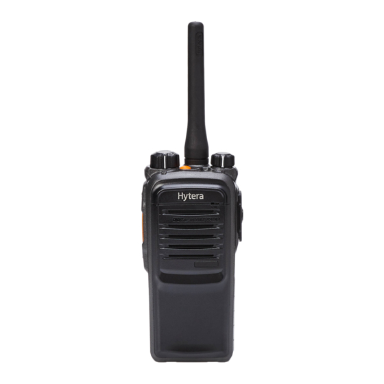
Page 9: Product Controls
Service Manual 5. Product Controls PD70X/ PD70XG/ HD705/ HD705G Part Name Part Name ○ SK1 (Side Key 1) ○ Radio On-Off/Volume Control Knob ○ PTT Key ○ Microphone ○ ○ SK2 (Side Key 2) Accessory Jack ○ ○ TK (Top Key) Battery Latch ○... - Page 10 Service Manual PD78X/ PD78XG/ HD785/ HD785G Part Name Part Name ○ ○ SK1 (Side Key 1) LED Indicator ○ ○ PTT Key Antenna ○ SK2 (Side Key 2) ○ Radio On-Off/Volume Control Knob ○ ○ TK (Top Key) Accessory Jack ○...
-
Page 11: Baseband Section
Service Manual 6. Baseband Section 6.1 Power Section 6.1.1 Diagram of Power Control Figure 6-1 Diagram of Power Control 6.1.2 Radio On/Off Figure 6-2 Diagram of Radio On/Off Control The radio-on signal (POWER-SW+) satisfies the equation: POWER-SW+= PWR-SW- | POWER-CTL. When the Volume Switch is on, PWR-SW- and POWER-SW+ are at high level, and the radio powers up. -
Page 12: Control Section
Service Manual After power-on, POWER-CTL goes to high level, and POWER-KEY-DET goes to low level. During power-off, POWER-SW+ is at low level, while POWER-KEY-DET is at high level. The system detects power-off procedure via POWER-KEY-DET and implements the power-off procedure. Then POWER-KEY-DET and POWER-SW+ go to low level, and the power is cut off. -
Page 13: External Memory
Service Manual Figure 6-4 Diagram of Overall Scheme 6.2.2 External Memory OMAP5912 provides two types of external memory interfaces: external memory interface slow (EMIFS) and external memory interface fast (EMIFF). OM AP5912 M T48H8M16LFB4-75 EM IFF EM IFS TV00570002CDGB SDRAM.A[0:12] A[0:12] FLASH.A[24:1] A[23:0]... - Page 14 Service Manual memories such as NAND Flash, NOR Flash and SRAM. 2) EMIFF EMIFF is a 16-bit interface, and supports SDRAM (up to 128MB), mobile SDRAM and mobile DDR. 6.2.3 Clock Option board CLK-32K-OUT CLK-OPT 32kHz 19.2MHz U201 OMAP5912 ULPD_PLL_CLK OSC32K_OUT CLK32K_IN 19.2MHz...
- Page 15 Service Manual 6.2.5 SPI OMAP5912 has a SPI, which has four chip-selects for connecting four external SPI components. The SPI signals available are SPI.DOUT, SPI.DIN, SPI.CLK and SPI.CS. The system uses SPIF.CS2 to select the IF processor AD9864, to configure register of AD9864. The connection of SPI is shown below. U201 OMAP5912 SPIF.CS2(T19)
- Page 16 Service Manual Figure 6-9 Diagram of MCBSP Connection 6.2.7 USB OMAP5912 provides 3 USB interfaces. One interface integrates a USB transceiver, which is connected to the accessory jack and is used for program downloading and data application. Figure 6-10 Diagram of USB Interface 6.2.8 UART OMAP5912 has three UART interfaces (UART1, UART2 and UART3), and supports hardware flow control.
- Page 17 Service Manual 6.2.9 I2C OMAP5912 provides one I2C interface, and supports communication rate up to 400Kbps. The I2C interface is connected with the acceleration sensor, and works in slave mode. The connection of I2C is shown below. Figure 6-12 Diagram of I2C Connection 6.2.10 MICROWIRE OMAP5912 provides a MICROWIRE.
-
Page 18: Audio Section
Service Manual 6.3 Audio Section 6.3.1 Audio Diagram The audio module is mainly for audio input and output. TLV320AIC29 is used as the audio codec to convert and process audio signal and digital signal. The audio amplifier TDA8547TS is used to amplify the analog audio signal. - Page 19 Service Manual sent to DSP for demodulation and processing. Then the digital signal is sent to the digital audio processor of the codec for digital audio processing, and is then converted into analog audio signal by DAC of the codec. Finally the signal is amplified by the external audio amplifier (TDA8547TS) to drive the speaker.
-
Page 20: Troubleshooting Flow Chart
Service Manual 6.4 Troubleshooting Flow Chart The GPS module The power supply for GPS is Replace the GPS outputs normally?[1] normal?[2] module. Check the power supply. The channel from GPS to Replace abnormal RC and OAMP is normal? check OMAP. L506 outputs 2.8V Replace the GPS PIN17 outputs 2.8V voltage? -
Page 21: Pcb Difference
Service Manual 6.5 PCB Difference For UHF1 PCB, Version H and Version K are made on the basis of Version F. 1. The following changes are made for Version H: Remove the board border and the small board. C802 is compatible with 1206 and 0805. 2. -
Page 22: Gps Circuit
Service Manual 7. GPS Circuit 7.1 Circuit Description Figure 7-1 Diagram of GPS Circuit The GPS function is realized via REB-1315LPx. The GPS circuit integrates a baseband processor, a LNA and a SAW. The 1575.42MHz GPS signal is received by the antenna, and then goes to HPF to remove the in-band signals used for transmission and reception. -
Page 23: Schematic Diagram
Service Manual 7.2 Schematic Diagram Figure 7-2 Schematic Diagram... -
Page 24: Parts List
Service Manual 7.3 Parts List No. Ref. No. Part No. Description C518 3101051590000 1.5P C519 3199050758000 0.75P C520 3101050100030 1P C527 3101050200010 2P C514 3101051210000 120P C516 3101051590070 1.5P C517 3101051800010 18P C522 3101051040060 0.1U C521 3101051210000 120P C512 3101054710010 470P C515 3101051050000 1UF C513... -
Page 25: Troubleshooting Flow Chart
Service Manual 7.4 Troubleshooting Flow Chart The GPS module The power supply for GPS is Replace the GPS outputs normally?[1] normal?[2] module. Check the power supply. The channel from GPS to Replace abnormal RC and OAMP is normal? check OMAP. L506 outputs 2.8V Replace the GPS PIN17 outputs 2.8V voltage? -
Page 26: Tuning Description
Service Manual 8. Tuning Description For details about radio tuning, please refer to the help file of DMR Tuner Software supplied by the Company. -
Page 27: Interface Definition
Service Manual 9. Interface Definition J1601: 50-Pin Interface Pin No. Name Function Valid Level 2、5、49 Power supply: ground (analog) AF-CODEC-TO-50PIN Analog audio signal output/input AF-50PIN-TO-CODEC EXT-MIC+ External MIC interface EXT-MIC- IO5-OPT IO4-OPT IO3-OPT GPIO pin of the option board IO2-OPT IO1-OPT 3V6D Power supply: 3.6V... - Page 28 Service Manual MCBSP3-DR-OPT IIC-SDA-Acce (for Version K of UHF1/UHF2/UHF3 and Version B IIC-SCL-Acce/CLK-32K-OUT of VHF) CLK-32K-OUT (for Version F/H of UHF1) IIC-SCL-Acce (for Version K of UHF1/UHF2/UHF3 and Version B IIC-SDA-Acce/CLK-OPT of VHF) CLK-32K-OUT (for Version F/H of UHF1) Power supply for accessory or EXT-BAT+ option board IN-SPK-...
- Page 29 Service Manual LED1 Red LED enable LED2 Green LED enable INT-MIC+780 Microphone+ INT-MIC-780 Microphone- NC/GND (for Version UHF1/UHF2/UHF3 and Version B of VHF) GND (for Version F/H of UHF1) PWR-SW- Power-on enable input PWR-SW+ Power-on enable output 3V3DRF 3.3V power supply NC/GND (for Version...
- Page 30 Service Manual AF-CODEC-TO-50PIN Analog audio signal Ground (digital) 3V6D Power supply for digital circuit 16-Pin Accessory Interface Pin No. Name Function Valid Level Ground (analog & digital) SPK- External speaker- SEL1-Accessory Accessory identifier 1 SEL2-Accessory Accessory identifier 2 Emergency Emergency SPK+ External speaker+ USB+ / RTS...
-
Page 31: Uhf1 (400-470Mhz) Information
Service Manual 10. UHF1 (400-470MHz) Information 10.1 Transmitter Circuit Figure 10-1 Diagram of Transmitter Circuit The transmitter circuit is mainly composed of: ① RF power amplifier circuit ② Low-pass filter circuit (for suppressing harmonics) ③ Auto power control circuit (APC) (including temperature detection circuit) The carrier signal generated by TX VCO is modulated and amplified, and then feeds to the transmitter circuit. -
Page 32: Receiver Circuit
Service Manual In the auto power control and temperature detection circuit, the drain current from the driver amplifier and final-stage amplifier is converted to voltage via the sampling resistor and subtraction circuit (composed of the first operational amplifier). This voltage is compared with the APC control voltage (output by DAC) at the second operational amplifier. - Page 33 Service Manual signal to the mixer. The wanted signal passes through the RF band-pass filter and low-noise amplifier and goes to the mixer (D9017). Meanwhile, the first local oscillator (LO) signal generated by VCO passes through the low-pass filter and also goes to the mixer (D9017). In the mixer, the wanted signal and the first LO signal are mixed to generate the first IF signal (73.35MHz).
-
Page 34: Frequency Generation Unit (Fgu)
Service Manual 10.3 Frequency Generation Unit (FGU) Figure 10-4 Diagram of FGU The FGU is composed of VCO and PLL. It is the core module of the whole TX-RX system. This circuit provides accurate carrier frequency during transmission, and stable LO signal during reception. It has a direct influence on the performance of the system. - Page 35 Service Manual output frequencies by changing the varactor's control voltage (i.e. CV voltage). There are two types of VCO: TX VCO and RX VCO. Both types control EMD22 to switch operating status via OMAP. RX VCO is composed of the oscillator loop and Q104, to provide LO signal. TX VCO is composed of the oscillator loop and Q108, to provide carrier for TX signal.
-
Page 36: Pcb View
10.4 PCB View PD70X/PD70XG/PD78X/PD78XG/HD705/HD705G/HD785/HD785G PCB View (Main Board) Top Layer... - Page 37 PD70X/PD70XG/PD78X/PD78XG/HD705/HD705G/HD785/HD785G PCB View (Main Board) Bottom Layer...
- Page 38 PD70X/PD70XG/HD705/HD705G PCB View (Channel Board) Top Layer...
- Page 39 PD70X/PD70XG/HD705/HD705G PCB View (Channel Board) Bottom Layer...
- Page 40 PD78X/PD78XG/HD785/HD785G PCB View (Channel Board) Top Layer...
- Page 41 PD78X/PD78XG/HD785/HD785G PCB View (Channel Board) Bottom Layer...
- Page 42 PD78X/PD78XG/HD785/HD785G PCB View (Keyboard) Top Layer...
- Page 43 PD78X/PD78XG/HD785/HD785G PCB View (Keyboard) Bottom Layer...
-
Page 44: Block Diagram
10.5 Block Diagram PD70X/PD70XG/PD78X/PD78XG/HD705/HD705G/HD785/HD785G Block Diagram (RF Section) Microstrip Low-pass Filter Tx/Rx Switch Pre-Drive2 Drive-stage Final-stage Pi Attenuator Pre-driver1 Matcher TV1/APC MOD1 Tx_VCO RX/TX RX/TX APC module VCO buffer amplifier TV1/APC 4CH DAC Rx_VCO Low-Noise Amp BATT+ Frequency Synthesizer module... - Page 45 PD70X/PD70XG/PD78X/PD78XG/HD705/HD705G/HD785/HD785G Block Diagram (Baseband Section)
- Page 46 PD70X/PD70XG/PD78X/PD78XG/HD705/HD705G/HD785/HD785G Block Diagram (Power Section) 1.6A/7.4V/5W RF PA 7.4V/1.6A RQA0002DNS 230mA/7.4V/Po=0.9W 1 /2 2.2V-18V 210mA/Po=0.89W/7.4V AF PA (TDA8547TS) 21mA/5VFGU TX:53mA/RX:29mA RX/TX 5VFGU 125uA-1000uA/5VFGU 5VA-RTC/ LDO: 5V VCCcp_main: Charge pump supply, 2.7V-5V(3 to 5 V); 150mA; VCO 3V3DRF VCCdigital: Digital supply, 2.7V-3V-3.3V;...
-
Page 47: Schematic Diagram
10.6 Schematic Diagram PD70X/PD70XG/PD78X/PD78XG/HD705/HD705G/HD785/HD785G Schematic Diagram (Transmitter/Receiver) PD780 UHF Schematic Diagram(TX/RX Circuit) C9002 C9002 L9002 L9002 100P 100P C9034 C9034 C9003 C9003 C9004 C9004 C9005 C9005 ANT1 ANT1 R9029 R9029 470P 470P C9009 C9009 TP9002 TP9002 C9020 C9020 C9012 C9012... - Page 48 PD780 UHF Schematic Diagram(CODEC Circuit) PD70X/PD70XG/PD78X/PD78XG/HD705/HD705G/HD785/HD785G Schematic Diagram (CODEC) 1V8D C834 C834 R829 R829 470K 470K AF-CODEC-IN TONE-CODEC 3 L821 L821 BLM15PD121SN1 BLM15PD121SN1 C837 C837 0.01u 0.01u C840 C840 C821 C821 R838 R838 0.22u 0.22u AF 50PIN to CODEC C846...
- Page 49 PD70X/PD70XG/PD78X/PD78XG/HD705/HD705G/HD785/HD785G Schematic Diagram (Audio Amplifier) PD780 UHF Schematic Diagram(AF Amplifier Circuit) BAT++ L802 L802 BLM18PG181SN1 BLM18PG181SN1 C803 C803 C804 C804 C802 C802 22u/10V 22u/10V 0.22u 0.22u 270P 270P L803 L803 EXT-SPK- R801 R801 R802 R802 C805 C805 R803 R803 C806...
- Page 50 PD70X/PD70XG/PD78X/PD78XG/HD705/HD705G/HD785/HD785G Schematic Diagram (DAC) PD780 UHF Schematic Diagram(DAC Circuit) 5VRT R712 R712 BLM15PD121SN1 BLM15PD121SN1 C705 C705 C706 C706 R709 R709 1000P 1000P 100k 100k C712 C712 R713 R713 R710 R710 100k 100k C703 C703 C704 C704 470P 470P TO VCO...
- Page 51 PD780 UHF Schematic Diagram(Power Circuit) PD70X/PD70XG/PD78X/PD78XG/HD705/HD705G/HD785/HD785G Schematic Diagram (Power) R607 100 R607 100 PWR-SW+ 5VFGU P607 P607 BAT++ 3V3ARF BAT+ U603 U603 L602 L602 J601 J601 L603 L603 RP102N331B RP102N331B L604 L604 F601 F601 BLM18PG181SN1 BLM18PG181SN1 R602 R602 R604 R604...
- Page 52 PD70X/PD70XG/PD78X/PD78XG/HD705/HD705G/HD785/HD785G Schematic Diagram (AD9864) PD780 UHF Schematic Diagram(AD9864 Circuit) TP402 TP402 TP403 TP403 L403 BLM15PD121SN1 L403 BLM15PD121SN1 L402 L402 TP401 TP401 C448 C448 2FLO 2FLO 270n 270n C420 C420 C457 C457 Q402 Q402 0.01u 0.01u TP404 TP404 L412 BLM15PD121SN1 L412 BLM15PD121SN1...
- Page 53 PD70X/PD70XG/PD78X/PD78XG/HD705/HD705G/HD785/HD785G Schematic Diagram (Internal Interface) PD780 UHF Schematic Diagram(INT Interface Circuit) 3V3D R314 R314 R315 R315 3.3K 3.3K D303 D303 D305 D305 3.3K 3.3K EXT-MIC+ AF CODEC TO 50PIN U310 U310 3V3D AF 50PIN to CODEC EXT-MIC- D304 D304 D306...
- Page 54 PD70X/PD70XG/PD78X/PD78XG/HD705/HD705G/HD785/HD785G Schematic Diagram (OMAP SI) PD780 UHF Schematic Diagram(OMAP SI Circuit) 3V3D R219 10K R219 10K 3V3D SYNCB-IF RN256 RN256 R256 R256 10K*4 10K*4 RN257 RN257 KB-R0 KP.R0/MPUIO8 KB-R1 SPI-CS2-IF SPIF.CS2/MPUIO4/uWIRE.CS2/LED2 KP.R1/MPUIO9 KB-R2 SPI-SCK-IF SPIF.SCK/MPUIO1 KP.R2/MPUIO10 KB-R3 SPI-DOUT-IF SPIF.DOUT/GPIO46/uWIRE.SDO KP.R3/MPUIO13...
- Page 55 PD780 UHF Schematic Diagram(OMAP MEM Circuit) PD70X/PD70XG/PD78X/PD78XG/HD705/HD705G/HD785/HD785G Schematic Diagram (OMAP MEN) M-A[1..24] U244 U244 SDRAM.A[0..12] U201A U201A SDRAM.A0 M-A1 M-A1 SDRAM.A0 FLASH.A1 1V8D SDRAM.A1 M-A2 M-A2 /CS2-LCD SDRAM.A1 FLASH.A2 SDRAM.A2 M-A3 M-A3 M-D0 /CS2-LCD R243 0 R243 0 M-A1 SDRAM.A2 FLASH.A3...
- Page 56 PD70X/PD70XG/PD78X/PD78XG/HD705/HD705G/HD785/HD785G Schematic Diagram (OMAP IO) PD780 UHF Schematic Diagram(OMAP IO Circuit) GPIO5/FLASH.CS2U POWER-KEY-DET 10 RESET-CODEC GPIO34/LCD.P13 POWER-CTL 10 GPIO7/UART2.RCV GPIO32/LCD.P11 IO to Accessory(TD TEST) GPIO8/TRST SEL1-ADC R212 100 R212 100 GPIO31/LCD.P10 GPIO16/FLASH.CS1U DISCHARGE-SW-TX 14 SEL2-ADC GPIO30/LCD.P9 EXT-PWR GPIO23/MCLKREQ DAV-CODEC GPIO29/LCD.P8 Acce-INT1 GPIO25/MCSI2.DOUT...
- Page 57 PD780 UHF Schematic Diagram(OMAP CORE Circuit) PD70X/PD70XG/PD78X/PD78XG/HD705/HD705G/HD785/HD785G Schematic Diagram (OMAP CORE) X201 X201 TP268 TP268 SSP-T7F 12.5pF 20ppm SEIKO SSP-T7F 12.5pF 20ppm SEIKO C205 C205 CLK-OMAP/IF C206 C206 X203 X203 C204 C204 C202 C202 1000P 1000P R213 R213 C203 C203...
- Page 58 PD70X/PD70XG/PD78X/PD78XG/HD705/HD705G/HD785/HD785G Schematic Diagram (FGU) PD780 UHF Schematic Diagram(FGU Circuit) 5VFGU C104 C104 470P 470P TP102 TP102 C102 C102 C103 C103 L101 L101 L104 L104 L105 L105 VCOFB VCOFB C106 C106 C105 C105 R102 R102 12nH(绕线) 12nH(绕线) 12nH(绕线) 12nH(绕线) 0.1u 0.1u...
- Page 59 PD70X/PD70XG/PD78X/PD78XG/HD705/HD705G/HD785/HD785G Schematic Diagram (External Interface) PD780 UHF Schematic Diagram(EXT Interface Circuit) J302 J302 R309 R309 USB-D- 5,7 PTT-IO USB-D+ 5,7 S302 S302 C307 C307 C325 C325 270p 270p 270p 270p nc-CON6 nc-CON6 J304 J304 NC*JTAG NC*JTAG RN302 100*4 RN302 100*4...
- Page 60 PD70X/PD70XG/HD705/HD705G Schematic Diagram (Channel Board) PD780 UHF Schematic Diagram(SW Board Circuit) D1002 D1002 3V3DRF S1001 S1001 S1002 S1002 Q1001 Q1001 12-22RG/TR8 12-22RG/TR8 R1001 120 R1001 120 LED1 PWR-SW+ PWR-SW- PWR-SW- VOL-H LED2 R1002 120 R1002 120 D1001 D1001 D1003 D1003...
- Page 61 PD780 UHF Schematic Diagram(SW Board Circuit) PD78X/PD78XG/HD785/HD785G Schematic Diagram (Channel Board) D1002 D1002 3V3DRF S1001 S1001 S1002 S1002 Q1001 Q1001 12-22RG/TR8 12-22RG/TR8 R1001 120 R1001 120 LED1 PWR-SW+ PWR-SW- PWR-SW- VOL-H LED2 R1002 120 R1002 120 D1001 D1001 D1003 D1003 D1005 D1005 D1007...
- Page 62 PD78X/PD78XG/HD785/HD785G Schematic Diagram (Keyboard) PD780 UHF Schematic Diagram(Keyboard Circuit) S1701 S1701 S1702 S1702 S1703 S1703 S1704 S1704 S1705 S1705 Cancel KB-R4 S1706 S1706 S1707 S1707 S1708 S1708 S1709 S1709 S1710 S1710 DOWN KB-R3 S1711 S1711 S1712 S1712 S1713 S1713 S1714 S1714 S1715 S1715...
-
Page 63: Parts List
Service Manual 10.7 Parts List Main Board for PD70X/ PD70XG/ PD78X/ PD78XG/ HD705/ HD705G/ HD785/ HD785G No. Ref. No. Part No. Description C9132 3001050000000 0Ω R135 3001050000000 0Ω R141 3001050000000 0Ω R204 3001050000000 0Ω R213 3001050000000 0Ω R243 3001050000000 0Ω... - Page 64 Service Manual No. Ref. No. Part No. Description R401 3001055100020 51Ω R9075 3001055100020 51Ω R101 3001055600000 56Ω R136 3001055600000 56Ω R503 3001051010000 100Ω R111 3001051010000 100Ω R119 3001051010000 100Ω R121 3001051010000 100Ω R205 3001051010000 100Ω R257 3001051010000 100Ω R327 3001051010000 100Ω...
- Page 65 Service Manual No. Ref. No. Part No. Description R9018 3001056810000 680Ω R416 3001058210000 820Ω R139 3001051020000 1KΩ R403 3001051020000 1KΩ R613 3001051020000 1KΩ R701 3001051020000 1KΩ R9033 3001051020000 1KΩ R9038 3001051020000 1KΩ R260 3001051520000 1.5KΩ R9008 3001051520000 1.5KΩ R9066 3001051520000 1.5KΩ...
- Page 66 Service Manual No. Ref. No. Part No. Description R9024 3001056820000 6.8KΩ R9067 3001056820000 6.8KΩ R110 3001058220000 8.2KΩ R118 3001058220000 8.2KΩ R407 3001058220000 8.2KΩ R9027 3001058220000 8.2KΩ R102 3001051030000 10KΩ R105 3001051030000 10KΩ R122 3001051030000 10KΩ R129 3001051030000 10KΩ R133 3001051030000 10KΩ...
- Page 67 Service Manual No. Ref. No. Part No. Description R145 3001053330000 33KΩ R146 3001053330000 33KΩ R707 3001053330000 33KΩ R830 3001053330000 33KΩ R9047 3001053330000 33KΩ R9079 3001053330000 33KΩ R627 3001054730010 47KΩ R628 3001054730010 47KΩ R630 3001054730010 47KΩ R826 3001054730010 47KΩ R9084 3001055630000 56KΩ...
- Page 68 Service Manual No. Ref. No. Part No. Description C147 3101060300010 C129 3101063690000 3.6PF C456 3101063690000 3.6PF C9021 3101063690000 3.6PF C106 3101050500010 C145 3101060500010 C146 3101060500010 C125 3101065690000 5.6PF C124 3101050600010 C9117 3101050600010 C9134 3101050600010 C123 3101060600010 C128 3101060600010 C108 3101050700010 C109 3101050700010 C114...
- Page 69 Service Manual No. Ref. No. Part No. Description C9120 3101051200020 12PF C9027 3101061200000 12PF C153 3101061300000 13PF C9079 3101051500020 15PF C9101 3101051500020 15PF C9105 3101051500020 15PF C9109 3101051500020 15PF C134 3101061500010 15PF C425 3101051800010 18PF C517 3101051800010 18PF C458 3101061800000 18PF C9112 3101061800000...
- Page 70 Service Manual No. Ref. No. Part No. Description C429 3101051010030 100PF C438 3101051010030 100PF C439 3101051010030 100PF C602 3101051010030 100PF C616 3101051010030 100PF C620 3101051010030 100PF C708 3101051010030 100PF C805 3101051010030 100PF C806 3101051010030 100PF C830 3101051010030 100PF C842 3101051010030 100PF C848 3101051010030...
- Page 71 Service Manual No. Ref. No. Part No. Description C471 3101052710000 270PF C652 3101052710000 270PF C680 3101052710000 270PF C681 3101052710000 270PF C685 3101052710000 270PF C709 3101052710000 270PF C804 3101052710000 270PF C807 3101052710000 270PF C811 3101052710000 270PF C814 3101052710000 270PF C818 3101052710000 270PF C829 3101052710000...
- Page 72 Service Manual No. Ref. No. Part No. Description C9075 3101054710010 470PF C9081 3101054710010 470PF C9096 3101054710010 470PF C9098 3101054710010 470PF C9013 3101064710000 470PF C137 3101051020010 1000PF C156 3101051020010 1000PF C161 3101051020010 1000PF C162 3101051020010 1000PF C163 3101051020010 1000PF C172 3101051020010 1000PF C180 3101051020010...
- Page 73 Service Manual No. Ref. No. Part No. Description C858 3101051520000 1500PF C9065 3101051520000 1500PF C159 3101052220010 2200PF C160 3101052220010 2200PF C431 3101052220010 2200PF C455 3101063320000 3300PF C215 3101051030020 0.01UF C174 3101051030020 0.01UF C251 3101051030020 0.01UF C426 3101051030020 0.01UF C436 3101051030020 0.01UF C440 3101051030020...
- Page 74 Service Manual No. Ref. No. Part No. Description C141 3101051040060 0.1UF C164 3101051040060 0.1UF C165 3101051040060 0.1UF C166 3101051040060 0.1UF C167 3101051040060 0.1UF C169 3101051040060 0.1UF C179 3101051040060 0.1UF C182 3101051040060 0.1UF C310 3101051040060 0.1UF C311 3101051040060 0.1UF C318 3101051040060 0.1UF C422 3101051040060...
- Page 75 Service Manual No. Ref. No. Part No. Description C679 3101051040060 0.1UF C682 3101051040060 0.1UF C688 3101051040060 0.1UF C710 3101051040060 0.1UF C801 3101051040060 0.1UF C809 3101051040060 0.1UF C810 3101051040060 0.1UF C812 3101051040060 0.1UF C817 3101051040060 0.1UF C833 3101051040060 0.1UF C836 3101051040060 0.1UF C839 3101051040060...
- Page 76 Service Manual No. Ref. No. Part No. Description C468 3104076840020 0.68UF C9041 3101051050000 C646 3110061050000 C657 3110061050000 C667 3110061050000 C154 3101051050000 C222 3101051050000 C229 3101051050000 C236 3101051050000 C247 3101051050000 C254 3101051050000 C312 3101051050000 C314 3101051050000 C323 3101051050000 C423 3101051050000 C515 3101051050000 C526 3101051050000...
- Page 77 Service Manual No. Ref. No. Part No. Description C641 3101062250000 2.2UF C649 3101062250000 2.2UF C660 3101062250000 2.2UF C670 3101062250000 2.2UF C825 3101062250000 2.2UF C828 3101062250000 2.2UF C603 3101074750000 4.7UF C621 3101074750000 4.7UF C636 3110071030000 Capacitor C661 3110071030000 Capacitor C802 3101082260020 22UF C9051 3104082260060...
- Page 78 Service Manual No. Ref. No. Part No. Description L9011 3210209102010 L607 3290299220000 Inductor L613 3290299220000 Inductor L615 3290299220000 Inductor L616 3290299220000 Inductor L411 3213212332000 3.3uH L408 3210407472000 4.7uH L413 3213306682000 6.8uH L614 3217099153000 15uH L610 3217099153000 15uH L502 3221506601080 Bead L505 3221506601080 Bead...
- Page 79 Service Manual No. Ref. No. Part No. Description L601 3221506181000 Bead L602 3221506181000 Bead L603 3221506181000 Bead L604 3221506181000 Bead L605 3221506181000 Bead L606 3221506181000 Bead L609 3221506181000 Bead L611 3221506181000 Bead L612 3221506181000 Bead L802 3221506181000 Bead R622 3221506181000 Bead F601 4099000000050...
- Page 80 Service Manual No. Ref. No. Part No. Description D9013 3399990000260 Rectifier diode D9017 3301250300000 Schottky barrier diode D307 3399040600020 ESD protection diode D308 3399040600020 ESD protection diode D309 3399040600020 ESD protection diode D310 3399040600020 ESD protection diode D602 3399040600020 ESD protection diode Q101 3401002000990 NPN transistor...
- Page 81 Service Manual No. Ref. No. Part No. Description U604 3608020005750 Power management IC U605 3608020005750 Power management IC U610 3608006000030 Power management IC U603 3608006000000 Power management IC U606 3608006000000 Power management IC U608 3608006000000 Power management IC U609 3608006000000 Power management IC U612 3608006000000...
- Page 82 Service Manual No. Ref. No. Part No. Description L9002 3210306820000 82nH R104 3001051020010 1KΩ R632 3001051020010 1KΩ C9128 3101050400010 C9133 3101050400010 C9135 3101050400010 C9136 3101050400010 C518 3101051590000 1.5PF C9100 3101052790000 2.7PF C176 3101053310030 330PF C208 3101053310030 330PF C9116 3101053690000 3.6PF C9087 3101054730000 0.047UF...
- Page 83 Service Manual No. Ref. No. Part No. Description R823 3001051030050 10KΩ R124 3001052720010 2.7KΩ R125 3001052720010 2.7KΩ R128 3001052720010 2.7KΩ R107 3001053310000 330Ω R9029 3001053310000 330Ω C443 3101063900000 39PF C816 3101071050020 L104 3290106120000 12nH L105 3290106120000 12nH C803 3101052240030 220nF C437 3101065620010 5600PF...
- Page 84 Service Manual No. Ref. No. Part No. Description L404 3217107103010 10uH U501 3609999000300 GPS LNA Z501 3804157560000 GPS filter R9045 3001051050000 1MΩ R9058 3001051050000 1MΩ R802 3001053340010 330KΩ R803 3001053340010 330KΩ R9002 3001054730000 47KΩ R9050 3001054730000 47KΩ R9007 3001058200000 82Ω C185 3104072250060 2.2UF...
- Page 85 Service Manual Channel Board for PD70X/ PD70XG/ HD705/ HD705G No. Ref. No. Part No. Description R1002 3001051210010 120Ω C1001 3101052710000 270PF C1002 3101052710000 270PF C1003 3101052710000 270PF C1004 3101052710000 270PF C1005 3101052710000 270PF C1006 3101052710000 270PF C1007 3101052710000 270PF C1010...
- Page 86 Service Manual Channel Board for PD78X/ PD78XG/ HD785/ HD785G No. Ref. No. Part No. Description R1002 3001051210010 120Ω C1001 3101052710000 270PF C1002 3101052710000 270PF C1003 3101052710000 270PF C1004 3101052710000 270PF C1005 3101052710000 270PF C1006 3101052710000 270PF C1007 3101052710000 270PF C1010 3101052710000 270PF C1011 3101052710000 270PF...
- Page 87 Service Manual Keyboard for PD78X/ PD78XG/ HD785/ HD785G No. Ref. No. Part No. Description 3001051010000 100Ω 3001051010000 100Ω 3001051010000 100Ω 3001051010000 100Ω 3001051010000 100Ω 3001051010000 100Ω 3001051010000 100Ω 3307990000260 LED 3307990000260 LED 3307990000260 LED 3307990000260 LED 3307990000260 LED 3307990000260 LED 3307990000260 LED 3310040000010 ESD protection diode 3310040000010 ESD protection diode...
-
Page 88: Troubleshooting Flow Chart
Service Manual 10.8 Troubleshooting Flow Chart Receiver Circuit... - Page 89 Service Manual Description of Normal Situations: [1] Output voltage by Q9019 PIN3: about 4.95V. [2] Output voltage by U605 PIN4 or input voltage into Q9019 PIN4: about 5V. [3] Vbe: about 0.74V; Vce: about 2.5V (in the case of no signal reception). [4] For Q9018, Vbe: about 0.76V;...
- Page 90 Service Manual Transmitter Circuit No power output Power supply Check the power works normally?[1] supply circuit. APC-OUT is APC-IN is Check the DAC normal?[2] normal?[3] output circuit. Replace Q9008 and Q9006. PS-TX and RT5V TX 5V voltage are normal?[5] is normal?[5] Check the power PS-APC 3.3V supply circuit.
- Page 91 Service Manual Description of Normal Situations: [1] Voltage of the power supply: about 7.4V. [2] For low power, APC-OUT: 1.8-2.1V; for high power, APC-OUT: 2.4-2.8V. [3] For low power, APC-IN: 1-1.3V; for high power, APC-IN: 1.8-2.1V. [4] PS-APC: about 3.3V. [5] TX5V: about 5V;...
- Page 92 Service Manual FGU check Check the power 5VFGU, 3V3ARF, supply circuit. 3V3DRF are normal? Q106 and Q107 Q104 and Q108 VCO oscillates? Replace Q104 are normal?[1] are normal?[2] and Q108. Check Q104, Q108 and Replace Q106 peripheral components. and Q107. Q106 、Q110 Replace L110 and L110 and L116 are...
- Page 93 Service Manual Description of Normal Situations: [1] During transmission, output voltage by Q107 PIN3: about 4V. During reception, output voltage by Q106 PIN3: about 4V. [2] During transmission, voltage at Q108 E: about 1.8V. During reception, voltage at Q104 E: about 1.8V. [3] The CV value varies with frequencies.
-
Page 94: Uhf2 (450-520Mhz) Information
Service Manual 11. UHF2 (450-520MHz) Information 11.1 Transmitter Circuit Figure 11-1 Diagram of Transmitter Circuit The transmitter circuit is mainly composed of: ① RF power amplifier circuit ② Low-pass filter circuit (for suppressing harmonics) ③ Auto power control circuit (APC) (including temperature detection circuit) The carrier signal generated by TX VCO is modulated and amplified, and then feeds to the transmitter circuit. -
Page 95: Receiver Circuit
Service Manual In the auto power control and temperature detection circuit, the drain current from the driver amplifier and final-stage amplifier is converted to voltage via the sampling resistor and subtraction circuit (composed of the first operational amplifier). This voltage is compared with the APC control voltage (output by DAC) at the second operational amplifier. - Page 96 Service Manual signal to the mixer. The wanted signal passes through the RF band-pass filter and low-noise amplifier and goes to the mixer (D9017). Meanwhile, the first local oscillator (LO) signal generated by VCO passes through the low-pass filter and also goes to the mixer (D9017). In the mixer, the wanted signal and the first LO signal are mixed to generate the first IF signal (73.35MHz).
-
Page 97: Frequency Generation Unit (Fgu)
Service Manual 11.3 Frequency Generation Unit (FGU) Figure 11-4 Diagram of FGU The FGU is composed of VCO and PLL. It is the core module of the whole TX-RX system. This circuit provides accurate carrier frequency during transmission, and stable LO signal during reception. It has a direct influence on the performance of the system. - Page 98 Service Manual output frequencies by changing the varactor's control voltage (i.e. CV voltage). There are two types of VCO: TX VCO and RX VCO. Both types control EMD22 to switch operating status via OMAP. RX VCO is composed of the oscillator loop and Q104, to provide LO signal. TX VCO is composed of the oscillator loop and Q108, to provide carrier for TX signal.
-
Page 99: Pcb View
11.4 PCB View PD70X/PD70XG/PD78X/PD78XG/HD705/HD705G/HD785/HD785G PCB View (Main Board) Top Layer... - Page 100 PD70X/PD70XG/PD78X/PD78XG/HD705/HD705G/HD785/HD785G PCB View (Main Board) Bottom Layer...
- Page 101 PD70X/PD70XG/HD705/HD705G PCB View (Channel Board) Top Layer...
- Page 102 PD70X/PD70XG/HD705/HD705G PCB View (Channel Board) Bottom Layer...
- Page 103 PD78X/PD78XG/HD785/HD785G PCB View (Channel Board) Top Layer...
- Page 104 PD78X/PD78XG/HD785/HD785G PCB View (Channel Board) Bottom Layer...
- Page 105 PD78X/PD78XG/HD785/HD785G PCB View (Keyboard) Top Layer...
- Page 106 PD78X/PD78XG/HD785/HD785G PCB View (Keyboard) Bottom Layer...
-
Page 107: Block Diagram
11.5 Block Diagram PD70X/PD70XG/PD78X/PD78XG/HD705/HD705G/HD785/HD785G Block Diagram (RF Section) Microstrip Low-pass Filter Tx/Rx Switch Pre-Drive2 Drive-stage Final-stage Pi Attenuator Pre-driver1 Matcher TV1/APC MOD1 Tx_VCO RX/TX RX/TX APC module VCO buffer amplifier TV1/APC 4CH DAC Rx_VCO Low-Noise Amp BATT+ Frequency Synthesizer module... - Page 108 PD70X/PD70XG/PD78X/PD78XG/HD705/HD705G/HD785/HD785G Block Diagram (Baseband Section)
- Page 109 PD70X/PD70XG/PD78X/PD78XG/HD705/HD705G/HD785/HD785G Block Diagram (Power Section) 1.6A/7.4V/5W RF PA 7.4V/1.6A RQA0002DNS 230mA/7.4V/Po=0.9W 1 /2 2.2V-18V 210mA/Po=0.89W/7.4V AF PA (TDA8547TS) 21mA/5VFGU TX:53mA/RX:29mA RX/TX 5VFGU 125uA-1000uA/5VFGU 5VA-RTC/ LDO: 5V VCCcp_main: Charge pump supply, 2.7V-5V(3 to 5 V); 150mA; VCO 3V3DRF VCCdigital: Digital supply, 2.7V-3V-3.3V;...
-
Page 110: Schematic Diagram
11.6 Schematic Diagram PD70X/PD70XG/PD78X/PD78XG/HD705/HD705G/HD785/HD785G Schematic Diagram (Transmitter/Receiver) 5VRT D9011 D9011 DAN222 DAN222 R9019 R9019 4.7K 4.7K C9002 C9002 L9002 L9002 100P 100P 2SA1832 2SA1832 C9054 C9054 C9034 C9034 Q9021 Q9021 R9020 R9020 C9003 C9003 C9004 C9004 C9005 C9005 0.75p 0.75p 1.5p... - Page 111 PD70X/PD70XG/PD78X/PD78XG/HD705/HD705G/HD785/HD785G Schematic Diagram (CODEC) 1V8D L821 L821 C834 C834 BLM15PD121SN1 BLM15PD121SN1 R829 R829 470K 470K AF-CODEC-IN TONE-CODEC 3 C837 C837 C821 C821 0.01u 0.01u 0.22u 0.22u C840 C840 R838 R838 R821 R821 AF-50PIN-TO-CODEC C846 C846 470P 470P C822 C822 C824...
- Page 112 PD70X/PD70XG/PD78X/PD78XG/HD705/HD705G/HD785/HD785G Schematic Diagram (Audio Amplifier) BAT+ L802 L802 BLM18PG181SN1 BLM18PG181SN1 C803 C803 C804 C804 C802 C802 10u/10V 10u/10V 0.22u 0.22u 270P 270P TP801 TP801 L803 L803 IN-SPK- R801 R801 R802 R802 C805 C805 R803 R803 C806 C806 150K 150K 220p...
- Page 113 PD70X/PD70XG/PD78X/PD78XG/HD705/HD705G/HD785/HD785G Schematic Diagram (DAC) 5VRT R712 R712 BLM15AG121SN1 BLM15AG121SN1 C705 C705 C706 C706 R709 R709 1000P 1000P 100k 100k C712 C712 R713 R713 R710 R710 100k 100k C703 C703 C704 C704 470P 470P 470p 470p R701 1K R701 1K MOD-VCO...
- Page 114 PD70X/PD70XG/PD78X/PD78XG/HD705/HD705G/HD785/HD785G Schematic Diagram (Power) 5VFGU R607 10 R607 10 P607 P607 3V3ARF BAT+ PWR-SW+ U603 U603 L602 L602 L603 L603 L604 L604 F601 F601 BLM18PG181SN1 BLM18PG181SN1 VOUT 3V3DRF BLM18PG181SN1 BLM18PG181SN1 C611 C611 2.5A-32V 2.5A-32V C606 C606 R631 15K R631 15K...
- Page 115 PD70X/PD70XG/PD78X/PD78XG/HD705/HD705G/HD785/HD785G Schematic Diagram (AD9864) TP402 TP402 TP403 TP403 L403 BLM15AG121SN1 L403 BLM15AG121SN1 L402 L402 TP401 TP401 C448 C448 2FLO 2FLO 270n 270n C420 C420 C457 C457 Q402 Q402 0.01u 0.01u TP404 TP404 R406 R406 L412 BLM15AG121SN1 L412 BLM15AG121SN1 PS-2LOC C446...
- Page 116 PD70X/PD70XG/PD78X/PD78XG/HD705/HD705G/HD785/HD785G Schematic Diagram (Internal Interface) 3V3D R314 R314 R315 R315 3.3K 3.3K D303 D303 D305 D305 3.3K 3.3K EXT-MIC+ AF-CODEC-TO-50PIN U310 U310 3V3D AF-50PIN-TO-CODEC EXT-MIC- D304 D304 D306 D306 DVdd_IO SLC/SPC IIC-SCL-Acce C311 C311 IIC-SDA-Acce SDA/SDI/SDO 0.1u 0.1u IADDR0 D318...
- Page 117 PD70X/PD70XG/PD78X/PD78XG/HD705/HD705G/HD785/HD785G Schematic Diagram (OMAP SI) 3V3D RN256 RN256 R256 R256 10K*4 10K*4 KB-R0 KP.R0/MPUIO8 KB-R1 SPI-CS2-IF SPIF.CS2/MPUIO4/uWIRE.CS2/LED2 KP.R1/MPUIO9 KB-R2 SPI-SCK-IF SPIF.SCK/MPUIO1 KP.R2/MPUIO10 KB-R3 SPI-DOUT-IF SPIF.DOUT/GPIO46/uWIRE.SDO KP.R3/MPUIO13 KB-R4 SPI-DIN-IF SPIF.DIN/GPIO47/uWIRE.SDI KP.R4/MPUIO15 C256 C256 C257 C257 C258 C258 C259 C259 470P 470P...
- Page 118 PD70X/PD70XG/PD78X/PD78XG/HD705/HD705G/HD785/HD785G Schematic Diagram (OMAP MEN) M-A[1..24] U244 U244 SDRAM.A[0..12] U201A U201A SDRAM.A0 M-A1 M-A1 SDRAM.A0 FLASH.A1 1V8D SDRAM.A1 M-A2 M-A2 /CS2-LCD SDRAM.A1 FLASH.A2 SDRAM.A2 M-A3 M-A3 M-D0 /CS2-LCD M-A1 SDRAM.A2 FLASH.A3 SDRAM.A3 M-A4 M-A4 M-D1 M-A1 SDRAM.A3 FLASH.A4 SDRAM.A4 M-A5...
- Page 119 PD70X/PD70XG/PD78X/PD78XG/HD705/HD705G/HD785/HD785G Schematic Diagram (OMAP IO) POWER-KEY-DET 10 GPIO5/FLASH.CS2U RESET-CODEC GPIO34/LCD.P13 POWER-CTL 10 GPIO7/UART2.RCV SEL-MIC GPIO32/LCD.P11 GPIO8/TRST IO-TD-TEST SEL1-ADC GPIO31/LCD.P10 DISCHARGE-SW-TX 14 GPIO16/FLASH.CS1U SEL2-ADC GPIO30/LCD.P9 EXT-PWR GPIO23/MCLKREQ C288 C288 C295 C295 470P 470P 470P 470P C298 C298 DAV-CODEC GPIO29/LCD.P8 470P 470P Acce-INT1 GPIO25/MCSI2.DOUT...
- Page 120 PD70X/PD70XG/PD78X/PD78XG/HD705/HD705G/HD785/HD785G Schematic Diagram (OMAP CORE) C205 C205 C206 C206 X203 X203 X201 X201 1000P 1000P SSP-T7F 12.5pF 20ppm SEIKO SSP-T7F 12.5pF 20ppm SEIKO 改良接地 CLK-OMAP/IF OE/ST OE/ST 470n 470n C202 C202 L201 L201 1000p 1000p C204 C204 C203 C203 C208...
- Page 121 PD70X/PD70XG/PD78X/PD78XG/HD705/HD705G/HD785/HD785G Schematic Diagram (FGU) 5VFGU C102 C102 C103 C103 4.7P 4.7P 4.7P 4.7P C104 C104 470P 470P L101 L101 C105 C105 TP102 TP102 L104 L104 L105 L105 0.1u 0.1u VCOFB VCOFB L102 L102 L103 L103 C106 C106 R102 R102 10nH(绕线) 10nH(绕线)
- Page 122 PD70X/PD70XG/PD78X/PD78XG/HD705/HD705G/HD785/HD785G Schematic Diagram (External Interface) PD780 UHF Schematic Diagram(EXT Interface Circuit) J302 J302 R309 R309 USB-D- 5,7 PTT-IO USB-D+ 5,7 S302 S302 C307 C307 C325 C325 270p 270p 270p 270p nc-CON6 nc-CON6 J304 J304 NC*JTAG NC*JTAG RN302 100*4 RN302 100*4...
- Page 123 PD70X/PD70XG/HD705/HD705G Schematic Diagram (Channel Board) PD780 UHF Schematic Diagram(SW Board Circuit) D1002 D1002 3V3DRF S1001 S1001 S1002 S1002 Q1001 Q1001 12-22RG/TR8 12-22RG/TR8 R1001 120 R1001 120 LED1 PWR-SW+ PWR-SW- PWR-SW- VOL-H LED2 R1002 120 R1002 120 D1001 D1001 D1003 D1003...
- Page 124 PD780 UHF Schematic Diagram(SW Board Circuit) PD78X/PD78XG/HD785/HD785G Schematic Diagram (Channel Board) D1002 D1002 3V3DRF S1001 S1001 S1002 S1002 Q1001 Q1001 12-22RG/TR8 12-22RG/TR8 R1001 120 R1001 120 LED1 PWR-SW+ PWR-SW- PWR-SW- VOL-H LED2 R1002 120 R1002 120 D1001 D1001 D1003 D1003 D1005 D1005 D1007...
- Page 125 PD78X/PD78XG/HD785/HD785G Schematic Diagram (Keyboard) PD780 UHF Schematic Diagram(Keyboard Circuit) S1701 S1701 S1702 S1702 S1703 S1703 S1704 S1704 S1705 S1705 Cancel KB-R4 S1706 S1706 S1707 S1707 S1708 S1708 S1709 S1709 S1710 S1710 DOWN KB-R3 S1711 S1711 S1712 S1712 S1713 S1713 S1714 S1714 S1715 S1715...
-
Page 126: Parts List
Service Manual 11.7 Parts List Main Board for PD70X/ PD70XG/ PD78X/ PD78XG/ HD705/ HD705G/ HD785/ HD785G Ref. No. Part No. Description R208 3001050000000 0Ω R254 3001050000000 0Ω R9069 3001050000000 0Ω C646 3001060000000 0Ω C657 3001060000000 0Ω C667 3001060000000 0Ω R9053 3099080398010 0.39Ω... - Page 127 Service Manual Ref. No. Part No. Description R121 3001051010000 100Ω R220 3001051010000 100Ω R221 3001051010000 100Ω R222 3001051010000 100Ω R224 3001051010000 100Ω R225 3001051010000 100Ω R226 3001051010000 100Ω R257 3001051010000 100Ω R408 3001051010000 100Ω R503 3001051010000 100Ω R704 3001051010000 100Ω R713 3001051010000 100Ω...
- Page 128 Service Manual Ref. No. Part No. Description R9033 3001051020000 1KΩ R9038 3001051020000 1KΩ R9040 3001051020000 1KΩ R612 3001061020010 1KΩ R260 3001051520000 1.5KΩ R9008 3001051520000 1.5KΩ R9066 3001051520000 1.5KΩ R413 3001051820000 1.8KΩ R820 3001052020020 2KΩ R825 3001052020020 2KΩ R832 3001052020020 2KΩ R833 3001052020020 2KΩ...
- Page 129 Service Manual Ref. No. Part No. Description R118 3001058220000 8.2KΩ R407 3001058220000 8.2KΩ R9027 3001058220000 8.2KΩ R102 3001051030000 10KΩ R105 3001051030000 10KΩ R129 3001051030000 10KΩ R133 3001051030000 10KΩ R142 3001051030000 10KΩ R241 3001051030000 10KΩ R242 3001051030000 10KΩ R249 3001051030000 10KΩ R256 3001051030000 10KΩ...
- Page 130 Service Manual Ref. No. Part No. Description R262 3001051530010 15KΩ R631 3001051530010 15KΩ R824 3001051530010 15KΩ R828 3001051530010 15KΩ R807 3001052030000 20KΩ RN261 3001052230020 22K*2 R145 3001053330000 33KΩ R146 3001053330000 33KΩ R707 3001053330000 33KΩ R830 3001053330000 33KΩ R9079 3001053330000 33KΩ R621 3001054730010 47KΩ...
- Page 131 Service Manual Ref. No. Part No. Description R829 3001054740010 470KΩ R9046 3001054740010 470KΩ R9059 3001054740010 470KΩ R9045 3001051050000 1MΩ R9058 3001051050000 1MΩ C171 3199050758000 0.75PF C519 3199050758000 0.75PF C520 3101050100030 C518 3101051590000 1.5PF C516 3101051590070 1.5PF C122 3101061590010 1.5PF C143 3101061590010 1.5PF C9004...
- Page 132 Service Manual Ref. No. Part No. Description C9109 3101050600010 C9124 3101050600010 C9131 3101050600010 C9137 3101050600010 C9023 3101060600010 C9024 3101060600010 C9028 3101050700010 C107 3101050800000 C119 3101050800000 C124 3101050800000 C9026 3101050800000 C9032 3101050800000 C9107 3101050800000 C9113 3101050800000 C9120 3101050800000 C9129 3101050800000 C9030 3101060800010 C9019 3101060900010...
- Page 133 Service Manual Ref. No. Part No. Description C9118 3101052700000 27PF C9122 3101052700000 27PF C460 3101063000010 30PF C448 3101053300000 33PF C461 3101063300000 33PF C443 3101063900000 39PF C9020 3101064300000 43PF C132 3101054700010 47PF C151 3101054700010 47PF C223 3101054700010 47PF C229 3101054700010 47PF C271 3101054700010 47PF...
- Page 134 Service Manual Ref. No. Part No. Description C262 3101052710000 270PF C270 3101052710000 270PF C285 3101052710000 270PF C290 3101052710000 270PF C291 3101052710000 270PF C292 3101052710000 270PF C321 3101052710000 270PF C322 3101052710000 270PF C325 3101052710000 270PF C326 3101052710000 270PF C334 3101052710000 270PF C469 3101052710000 270PF...
- Page 135 Service Manual Ref. No. Part No. Description C281 3101054710010 470PF C282 3101054710010 470PF C283 3101054710010 470PF C284 3101054710010 470PF C287 3101054710010 470PF C288 3101054710010 470PF C293 3101054710010 470PF C294 3101054710010 470PF C295 3101054710010 470PF C296 3101054710010 470PF C297 3101054710010 470PF C298 3101054710010 470PF...
- Page 136 Service Manual Ref. No. Part No. Description C849 3101054710010 470PF C851 3101054710010 470PF C853 3101054710010 470PF C856 3101054710010 470PF C857 3101054710010 470PF C9018 3101054710010 470PF C9029 3101054710010 470PF C9033 3101054710010 470PF C9034 3101054710010 470PF C9037 3101054710010 470PF C9039 3101054710010 470PF C9042 3101054710010 470PF...
- Page 137 Service Manual Ref. No. Part No. Description C9088 3101051020010 1000PF C9089 3101051020010 1000PF C9093 3101051020010 1000PF C9103 3101051020010 1000PF C9121 3101051020010 1000PF C9123 3101051020010 1000PF C9060 3101061020000 1000PF L9039 3101061020000 1000PF C275 3101051520000 1500PF C276 3101051520000 1500PF C277 3101051520000 1500PF C289 3101051520000 1500PF...
- Page 138 Service Manual Ref. No. Part No. Description C426 3101051030020 0.01UF C436 3101051030020 0.01UF C440 3101051030020 0.01UF C447 3101051030020 0.01UF C449 3101051030020 0.01UF C453 3101051030020 0.01UF C454 3101051030020 0.01UF C457 3101051030020 0.01UF C647 3101051030020 0.01UF C651 3101051030020 0.01UF C668 3101051030020 0.01UF C819 3101051030020 0.01UF...
- Page 139 Service Manual Ref. No. Part No. Description C434 3101051040060 0.1UF C435 3101051040060 0.1UF C441 3101051040060 0.1UF C445 3101051040060 0.1UF C446 3101051040060 0.1UF C462 3101051040060 0.1UF C464 3101051040060 0.1UF C465 3101051040060 0.1UF C466 3101051040060 0.1UF C522 3101051040060 0.1UF C523 3101051040060 0.1UF C525 3101051040060 0.1UF...
- Page 140 Service Manual Ref. No. Part No. Description C9043 3101051040060 0.1UF C9046 3101051040060 0.1UF C9049 3101051040060 0.1UF C9057 3101051040060 0.1UF C9071 3101051040060 0.1UF C9080 3101051040060 0.1UF C9086 3101051040060 0.1UF C9091 3101051040060 0.1UF C9092 3101051040060 0.1UF C9097 3101051040060 0.1UF C9104 3101051040060 0.1UF C212 3101052240010 0.22UF...
- Page 141 Service Manual Ref. No. Part No. Description C706 3101051050000 C707 3101051050000 C711 3101051050000 C712 3101051050000 C831 3101051050000 C832 3101051050000 C834 3101051050000 C840 3101051050000 C847 3101051050000 C9052 3101051050000 C9095 3101051050000 C605 3101061050020 C623 3101061050020 C648 3101061050020 C669 3101061050020 C677 3101061050020 C701 3101061050020 C816 3101061050020...
- Page 142 Service Manual Ref. No. Part No. Description L801 3221505121010 Bead L803 3221505121010 Bead L804 3221505121010 Bead L805 3221505121010 Bead L821 3221505121010 Bead L822 3221505121010 Bead L9015 3221505121010 Bead L9020 3221505121010 Bead L302 3221506601000 Bead L304 3221506601000 Bead L305 3221506601000 Bead L410 3221506601000 Bead...
- Page 143 Service Manual Ref. No. Part No. Description L103 3212106100000 10nH L9018 3210106150000 15nH L9033 3237199170000 17nH L9035 3237199170000 17nH L9036 3237199170000 17nH L9037 3237199170000 17nH L507 3210305180000 18nH L117 3217107120000 12nH L112 3217107160000 16nH L9017 3217106180010 18nH L9028 3210106220000 22nH L9009 3210306150000 15nH...
- Page 144 Service Manual Ref. No. Part No. Description L404 3215099103000 10uH L610 3217099153000 15uH L614 3217099153000 15uH D302 3303990000010 Switching diode D601 3399990000110 Diode D9002 3303030800040 Switching diode D111 3304010100890 Varactor D101 3304010100220 Varactor D102 3304010100220 Varactor D103 3304010100220 Varactor D106 3304010100220 Varactor D107...
- Page 145 Service Manual Ref. No. Part No. Description Q9004 3406001000090 NPN transistor Q101 3401002000990 NPN transistor Q604 3503020000030 N-MOSFET Q607 3503020000030 N-MOSFET Q608 3503020000030 N-MOSFET Q9001 3418001000010 NPN transistor Q310 3511990000010 N-MOSFET Q313 3511990000010 N-MOSFET Q312 3403008000010 Q801 3403008000010 Q802 3403008000010 Q9007 3403008000010 Q9008...
- Page 146 Service Manual Ref. No. Part No. Description U611 3608011000050 DC-DC U242 3612044000010 Memory U9002 3605025000020 Operational amplifier U820 3616037000020 Switch U201 3610010000010 U610 3608006000030 Power management IC U606 3608006000000 Power management IC U608 3608006000000 Power management IC U609 3608006000000 Power management IC U612 3608006000000 Power management IC...
- Page 147 Service Manual Ref. No. Part No. Description R9023 3001053920010 3.9KΩ R9047 3001053920010 3.9KΩ C159 3101052220010 2200pF C160 3101052220010 2200pF C431 3101052220010 2200pF C102 3101054790010 4.7PF C103 3101054790010 4.7PF C111 3101054790010 4.7PF C112 3101054790010 4.7PF C130 3101062700010 27PF C9007 3101060700020 C152 3101060500010 C452 3101060500010...
- Page 148 Service Manual Ref. No. Part No. Description R125 3001051220090 1.2KΩ R9056 3001051240010 120KΩ R123 3001051840010 180KΩ C154 3001052220010 2.2KΩ R122 3001053320010 3.3KΩ R120 3001054790010 4.7KΩ R601 3001059130000 91KΩ C608 3101051050160 C9111 3101050690050 C149 3101060200010 C458 3101061800000 18PF 6201810000000 Shielding can for baseband processor 6201860000000 Shielding frame for GPS 6201865000000...
- Page 149 Service Manual Channel Board for PD70X/ PD70XG/ HD705/ HD705G Ref. No. Part No. Description R1002 3001051210010 120Ω C1001 3101052710000 270PF C1002 3101052710000 270PF C1003 3101052710000 270PF C1004 3101052710000 270PF C1005 3101052710000 270PF C1006 3101052710000 270PF C1007 3101052710000 270PF C1010 3101052710000...
- Page 150 Service Manual Channel Board for PD78X/ PD78XG/ HD785/ HD785G Ref. No. Part No. Description R1002 3001051210010 120Ω C1001 3101052710000 270PF C1002 3101052710000 270PF C1003 3101052710000 270PF C1004 3101052710000 270PF C1005 3101052710000 270PF C1006 3101052710000 270PF C1007 3101052710000 270PF C1010 3101052710000 270PF C1011 3101052710000...
- Page 151 Service Manual Keyboard for PD78X/ PD78XG/ HD785/ HD785G Ref. No. Part No. Description 3001051010000 100Ω 3001051010000 100Ω 3001051010000 100Ω 3001051010000 100Ω 3001051010000 100Ω 3001051010000 100Ω 3001051010000 100Ω 3307990000260 3307990000260 3307990000260 3307990000260 3307990000260 3307990000260 3307990000260 3310040000010 ESD protection diode 3310040000010 ESD protection diode 5201016000010 Board-to-board connector...
-
Page 152: Troubleshooting Flow Chart
Service Manual 11.8 Troubleshooting Flow Chart Receiver Circuit... - Page 153 Service Manual Description of Normal Situations: [1] Output voltage by Q9019 PIN3: about 4.95V. [2] Output voltage by U605 PIN4 or input voltage into Q9019 PIN4: about 5V. [3] Vbe: about 0.74V; Vce: about 2.5V (in the case of no signal reception). [4] For Q9018, Vbe: about 0.76V;...
- Page 154 Service Manual Transmitter Circuit No power output Power supply Check the power works normally?[1] supply circuit. APC-OUT is APC-IN is Check the DAC normal?[2] normal?[3] output circuit. Replace Q9008 and Q9006. PS-TX and RT5V TX 5V voltage are normal?[5] is normal?[5] Check the power PS-APC 3.3V supply circuit.
- Page 155 Service Manual Description of Normal Situations: [1] Voltage of the power supply: about 7.4V. [2] For low power, APC-OUT: 1.8-2.1V; for high power, APC-OUT: 2.4-2.8V. [3] For low power, APC-IN: 1-1.3V; for high power, APC-IN: 1.8-2.1V. [4] PS-APC: about 3.3V. [5] TX5V: about 5V;...
- Page 156 Service Manual FGU check Check the power 5VFGU, 3V3ARF, supply circuit. 3V3DRF are normal? Q106 and Q107 Q104 and Q108 VCO oscillates? Replace Q104 are normal?[1] are normal?[2] and Q108. Check Q104, Q108 and Replace Q106 peripheral components. and Q107. Q106 、Q110 Replace L110 and L110 and L116 are...
- Page 157 Service Manual Description of Normal Situations: [1] During transmission, output voltage by Q107 PIN3: about 4V. During reception, output voltage by Q106 PIN3: about 4V. [2] During transmission, voltage at Q108 E: about 1.8V. During reception, voltage at Q104 E: about 1.8V. [3] The CV value varies with frequencies.
-
Page 158: Uhf3 (350-400Mhz) Information
Service Manual 12. UHF3 (350-400MHz) Information 12.1 Transmitter Circuit Figure 12-1 Diagram of Transmitter Circuit The transmitter circuit is mainly composed of: ① RF power amplifier circuit ② Low-pass filter circuit (for suppressing harmonics) ③ Auto power control circuit (APC) (including temperature detection circuit) The carrier signal generated by TX VCO is modulated and amplified, and then feeds to the transmitter circuit. -
Page 159: Receiver Circuit
Service Manual In the auto power control and temperature detection circuit, the drain current from the driver amplifier and final-stage amplifier is converted to voltage via the sampling resistor and subtraction circuit (composed of the first operational amplifier). This voltage is compared with the APC control voltage (output by DAC) at the second operational amplifier. - Page 160 Service Manual level, to remove out-of-band interference signal generated during amplification, and to send wanted HF signal to the mixer. The wanted signal passes through the RF band-pass filter and low-noise amplifier and goes to the mixer (D9017). Meanwhile, the first local oscillator (LO) signal generated by VCO passes through the low-pass filter and also goes to the mixer (D9017).
-
Page 161: Frequency Generation Unit (Fgu)
Service Manual 12.3 Frequency Generation Unit (FGU) Figure 12-4 Diagram of FGU The FGU is composed of VCO and PLL. It is the core module of the whole TX-RX system. This circuit provides accurate carrier frequency during transmission, and stable LO signal during reception. It has a direct influence on the performance of the system. - Page 162 Service Manual output frequencies by changing the varactor's control voltage (i.e. CV voltage). There are two types of VCO: TX VCO and RX VCO. Both types control EMD22 to switch operating status via OMAP. RX VCO is composed of the oscillator loop and Q104, to provide LO signal. TX VCO is composed of the oscillator loop and Q108, to provide carrier for TX signal.
-
Page 163: Pcb View
12.4 PCB View PD70X/PD70XG/PD78X/PD78XG/HD705/HD705G/HD785/HD785G PCB View (Main Board) Top Layer... - Page 164 PD70X/PD70XG/PD78X/PD78XG/HD705/HD705G/HD785/HD785G PCB View (Main Board) Bottom Layer...
- Page 165 PD70X/PD70XG/HD705/HD705G PCB View (Channel Board) Top Layer...
- Page 166 PD70X/PD70XG/HD705/HD705G PCB View (Channel Board) Bottom Layer...
- Page 167 PD78X/PD78XG/HD785/HD785G PCB View (Channel Board) Top Layer...
- Page 168 PD78X/PD78XG/HD785/HD785G PCB View (Channel Board) Bottom Layer...
- Page 169 PD78X/PD78XG/HD785/HD785G PCB View (Keyboard) Top Layer...
- Page 170 PD78X/PD78XG/HD785/HD785G PCB View (Keyboard) Bottom Layer...
-
Page 171: Block Diagram
12.5 Block Diagram PD70X/PD70XG/PD78X/PD78XG/HD705/HD705G/HD785/HD785G Block Diagram (RF Section) Microstrip Low-pass Filter Tx/Rx Switch Pre-Drive2 Drive-stage Final-stage Pi Attenuator Pre-driver1 Matcher TV1/APC MOD1 Tx_VCO RX/TX RX/TX APC module VCO buffer amplifier TV1/APC 4CH DAC Rx_VCO Low-Noise Amp BATT+ Frequency Synthesizer module... - Page 172 PD70X/PD70XG/PD78X/PD78XG/HD705/HD705G/HD785/HD785G Block Diagram (Baseband Section)
- Page 173 PD70X/PD70XG/PD78X/PD78XG/HD705/HD705G/HD785/HD785G Block Diagram (Power Section) 1.6A/7.4V/5W RF PA 7.4V/1.6A RQA0002DNS 230mA/7.4V/Po=0.9W 1 /2 2.2V-18V 210mA/Po=0.89W/7.4V AF PA (TDA8547TS) 21mA/5VFGU TX:53mA/RX:29mA RX/TX 5VFGU 125uA-1000uA/5VFGU 5VA-RTC/ LDO: 5V VCCcp_main: Charge pump supply, 2.7V-5V(3 to 5 V); 150mA; VCO 3V3DRF VCCdigital: Digital supply, 2.7V-3V-3.3V;...
-
Page 174: Schematic Diagram
12.6 Schematic Diagram PD70X/PD70XG/PD78X/PD78XG/HD705/HD705G/HD785/HD785G Schematic Diagram (Transmitter/Receiver) 5VRT D9011 D9011 DAN222 DAN222 R9019 R9019 4.7K 4.7K C9002 C9002 L9002 L9002 100P 100P 2SA1832 2SA1832 C9054 C9054 C9034 C9034 Q9021 Q9021 R9020 R9020 C9003 C9003 C9004 C9004 C9005 C9005 0.5p 0.5p 1.5p... - Page 175 PD70X/PD70XG/PD78X/PD78XG/HD705/HD705G/HD785/HD785G Schematic Diagram (CODEC) 1V8D L821 L821 C834 C834 BLM15PD121SN1 BLM15PD121SN1 R829 R829 470K 470K AF-CODEC-IN TONE-CODEC 3 C837 C837 C821 C821 0.01u 0.01u 0.22u 0.22u C840 C840 R838 R838 AF-50PIN-TO-CODEC R821 R821 C846 C846 470P 470P C822 C822 C824...
- Page 176 PD70X/PD70XG/PD78X/PD78XG/HD705/HD705G/HD785/HD785G Schematic Diagram (Audio Amplifier) BAT+ L802 L802 BLM18PG181SN1 BLM18PG181SN1 C803 C803 C804 C804 C802 C802 10u/10V 10u/10V 0.22u 0.22u 270P 270P TP801 TP801 L803 L803 IN-SPK- R801 R801 R802 R802 C805 C805 R803 R803 C806 C806 150K 150K 220p...
- Page 177 PD70X/PD70XG/PD78X/PD78XG/HD705/HD705G/HD785/HD785G Schematic Diagram (DAC) 5VRT R712 R712 BLM15AG121SN1 BLM15AG121SN1 C705 C705 C706 C706 R709 R709 1000P 1000P 100k 100k C712 C712 R713 R713 R710 R710 100k 100k C703 C703 C704 C704 470P 470P 470p 470p R701 1K R701 1K MOD-VCO...
- Page 178 PD70X/PD70XG/PD78X/PD78XG/HD705/HD705G/HD785/HD785G Schematic Diagram (Power) 5VFGU P607 P607 R607 R607 3V3ARF BAT+ U603 U603 PWR-SW+ L602 L602 L604 L604 L603 L603 RP102N331B*NC RP102N331B*NC F601 F601 BLM18PG181SN1 BLM18PG181SN1 VOUT 3V3DRF BLM18PG181SN1*NC BLM18PG181SN1*NC BLM18PG181SN1 BLM18PG181SN1 C611 C611 2.5A-32V 2.5A-32V C606 C606 R631 15K...
- Page 179 PD70X/PD70XG/PD78X/PD78XG/HD705/HD705G/HD785/HD785G Schematic Diagram (AD9864) TP402 TP402 TP403 TP403 L403 BLM15AG121SN1 L403 BLM15AG121SN1 L402 L402 TP401 TP401 C448 C448 2FLO 2FLO 270n 270n C420 C420 C457 C457 Q402 Q402 0.01u 0.01u TP404 TP404 R406 R406 L412 BLM15AG121SN1 L412 BLM15AG121SN1 PS-2LOC C446...
- Page 180 PD70X/PD70XG/PD78X/PD78XG/HD705/HD705G/HD785/HD785G Schematic Diagram (Internal Interface) 3V3D D303 D303 D305 D305 EXT-MIC+ R314 R314 AF-CODEC-TO-50PIN R315 R315 AF-50PIN-TO-CODEC 3.3K 3.3K EXT-MIC- 3.3K 3.3K D304 D304 D306 D306 U310 U310 3V3D D318 D318 DVdd_IO SLC/SPC IIC-SCL-Acce C311 C311 IIC-SDA-Acce SDA/SDI/SDO 0.1u 0.1u...
- Page 181 PD70X/PD70XG/PD78X/PD78XG/HD705/HD705G/HD785/HD785G Schematic Diagram (OMAP SI) 3V3D RN256 RN256 R256 R256 10K*4 10K*4 KB-R0 KP.R0/MPUIO8 KB-R1 SPI-CS2-IF SPIF.CS2/MPUIO4/uWIRE.CS2/LED2 KP.R1/MPUIO9 KB-R2 SPI-SCK-IF SPIF.SCK/MPUIO1 KP.R2/MPUIO10 KB-R3 SPI-DOUT-IF SPIF.DOUT/GPIO46/uWIRE.SDO KP.R3/MPUIO13 KB-R4 SPI-DIN-IF SPIF.DIN/GPIO47/uWIRE.SDI KP.R4/MPUIO15 C256 C256 C257 C257 C258 C258 C259 C259 470P 470P...
- Page 182 PD70X/PD70XG/PD78X/PD78XG/HD705/HD705G/HD785/HD785G Schematic Diagram (OMAP MEN) M-A[1..24] U244 U244 SDRAM.A[0..12] U201A U201A SDRAM.A0 M-A1 M-A1 SDRAM.A0 FLASH.A1 1V8D SDRAM.A1 M-A2 M-A2 /CS2-LCD SDRAM.A1 FLASH.A2 SDRAM.A2 M-A3 M-A3 M-D0 /CS2-LCD M-A1 SDRAM.A2 FLASH.A3 SDRAM.A3 M-A4 M-A4 M-D1 M-A1 SDRAM.A3 FLASH.A4 SDRAM.A4 M-A5...
- Page 183 PD70X/PD70XG/PD78X/PD78XG/HD705/HD705G/HD785/HD785G Schematic Diagram (OMAP IO) POWER-KEY-DET 10 GPIO5/FLASH.CS2U RESET-CODEC GPIO34/LCD.P13 POWER-CTL 10 GPIO7/UART2.RCV SEL-MIC GPIO32/LCD.P11 GPIO8/TRST IO-TD-TEST SEL1-ADC GPIO31/LCD.P10 DISCHARGE-SW-TX 14 GPIO16/FLASH.CS1U SEL2-ADC GPIO30/LCD.P9 EXT-PWR GPIO23/MCLKREQ C288 C288 C295 C295 470P 470P 470P 470P C298 C298 DAV-CODEC GPIO29/LCD.P8 470P 470P Acce-INT1 GPIO25/MCSI2.DOUT...
- Page 184 PD70X/PD70XG/PD78X/PD78XG/HD705/HD705G/HD785/HD785G Schematic Diagram (OMAP CORE) C205 C205 C206 C206 X203 X203 X201 X201 1000P 1000P SSP-T7F 12.5pF 20ppm SEIKO SSP-T7F 12.5pF 20ppm SEIKO CLK-OMAP/IF OE/ST OE/ST 470n 470n C202 C202 L201 L201 1000p 1000p C204 C204 C203 C203 C208 C208...
- Page 185 PD70X/PD70XG/PD78X/PD78XG/HD705/HD705G/HD785/HD785G Schematic Diagram (FGU) C102 C102 C103 C103 5VFGU C104 C104 470P 470P TP102 TP102 L101 L101 C105 C105 L104 L104 VCOFB VCOFB L102 L102 L103 L103 C106 C106 L105 L105 R102 R102 0.1u 0.1u 15nH(绕线) 15nH(绕线) 15nH(绕线) 15nH(绕线) U102...
- Page 186 PD70X/PD70XG/PD78X/PD78XG/HD705/HD705G/HD785/HD785G Schematic Diagram (External Interface) PD780 UHF Schematic Diagram(EXT Interface Circuit) J302 J302 R309 R309 USB-D- 5,7 PTT-IO USB-D+ 5,7 S302 S302 C307 C307 C325 C325 270p 270p 270p 270p nc-CON6 nc-CON6 J304 J304 NC*JTAG NC*JTAG RN302 100*4 RN302 100*4...
- Page 187 PD70X/PD70XG/HD705/HD705G Schematic Diagram (Channel Board) PD780 UHF Schematic Diagram(SW Board Circuit) D1002 D1002 3V3DRF S1001 S1001 S1002 S1002 Q1001 Q1001 12-22RG/TR8 12-22RG/TR8 R1001 120 R1001 120 LED1 PWR-SW+ PWR-SW- PWR-SW- VOL-H LED2 R1002 120 R1002 120 D1001 D1001 D1003 D1003...
- Page 188 PD780 UHF Schematic Diagram(SW Board Circuit) PD78X/PD78XG/HD785/HD785G Schematic Diagram (Channel Board) D1002 D1002 3V3DRF S1001 S1001 S1002 S1002 Q1001 Q1001 12-22RG/TR8 12-22RG/TR8 R1001 120 R1001 120 LED1 PWR-SW+ PWR-SW- PWR-SW- VOL-H LED2 R1002 120 R1002 120 D1001 D1001 D1003 D1003 D1005 D1005 D1007...
- Page 189 PD780 UHF Schematic Diagram(Keyboard Circuit) PD78X/PD78XG/HD785/HD785G Schematic Diagram (Keyboard) S1701 S1701 S1702 S1702 S1703 S1703 S1704 S1704 S1705 S1705 Cancel KB-R4 S1706 S1706 S1707 S1707 S1708 S1708 S1709 S1709 S1710 S1710 DOWN KB-R3 S1711 S1711 S1712 S1712 S1713 S1713 S1714 S1714 S1715 S1715...
-
Page 190: Parts List
Service Manual 12.7 Parts List Main Board for PD70X/ PD70XG/ PD78X/ PD78XG/ HD705/ HD705G/ HD785/ HD785G No. Ref. No. Part No. Description R208 3001050000000 0Ω R254 3001050000000 0Ω R9069 3001050000000 0Ω C157 3001060000000 0Ω C646 3001060000000 0Ω C657 3001060000000 0Ω... - Page 191 Service Manual No. Ref. No. Part No. Description R220 3001051010000 100Ω R221 3001051010000 100Ω R222 3001051010000 100Ω R224 3001051010000 100Ω R225 3001051010000 100Ω R257 3001051010000 100Ω R408 3001051010000 100Ω R503 3001051010000 100Ω R704 3001051010000 100Ω R713 3001051010000 100Ω R821 3001051010000 100Ω...
- Page 192 Service Manual No. Ref. No. Part No. Description R9033 3001051020000 1KΩ R9038 3001051020000 1KΩ R9040 3001051020000 1KΩ R612 3001061020010 1KΩ R260 3001051520000 1.5KΩ R9008 3001051520000 1.5KΩ R9066 3001051520000 1.5KΩ R820 3001052020020 2KΩ R825 3001052020020 2KΩ R832 3001052020020 2KΩ R833 3001052020020 2KΩ...
- Page 193 Service Manual No. Ref. No. Part No. Description R9089 3001055620000 5.6KΩ R9024 3001056820000 6.8KΩ R9067 3001056820000 6.8KΩ R110 3001058220000 8.2KΩ R118 3001058220000 8.2KΩ R407 3001058220000 8.2KΩ R9027 3001058220000 8.2KΩ R102 3001051030000 10KΩ R105 3001051030000 10KΩ R129 3001051030000 10KΩ R133 3001051030000 10KΩ...
- Page 194 Service Manual No. Ref. No. Part No. Description C158 3001061030010 10KΩ R410 3001061030010 10KΩ R415 3001061030010 10KΩ RN256 3005051030010 10KΩ R261 3001051530010 15KΩ R262 3001051530010 15KΩ R631 3001051530010 15KΩ R824 3001051530010 15KΩ R828 3001051530010 15KΩ R807 3001052030000 20KΩ RN261 3001052230020 22K*2 R145 3001053330000...
- Page 195 Service Manual No. Ref. No. Part No. Description R813 3001051540000 150KΩ R814 3001051540000 150KΩ R9048 3001051540000 150KΩ R9057 3001051540000 150KΩ R112 3001051840000 180KΩ R617 3001054740010 470KΩ R829 3001054740010 470KΩ R9046 3001054740010 470KΩ R9059 3001054740010 470KΩ R9045 3001051050000 1MΩ R9058 3001051050000 1MΩ...
- Page 196 Service Manual No. Ref. No. Part No. Description C9030 3101060700020 C107 3101050800000 C108 3101050800000 C109 3101050800000 C114 3101050800000 C9035 3101050800000 C115 3101050800000 C9026 3101050800000 C9032 3101050800000 C9107 3101050800000 C9113 3101050800000 C9023 3101060800010 C9024 3101060800010 C9009 3101060900010 C9019 3101060900010 C119 3101051000020 10PF C9025 3101051000020...
- Page 197 Service Manual No. Ref. No. Part No. Description C644 3101052000020 20PF C672 3101052000020 20PF C9079 3101052000020 20PF C432 3101052200010 22PF C9106 3101052200010 22PF C148 3101062200010 22PF C9112 3101062200010 22PF C9001 3101052700000 27PF C9118 3101052700000 27PF C9122 3101052700000 27PF C134 3101062700010 27PF C460 3101063000010...
- Page 198 Service Manual No. Ref. No. Part No. Description C709 3101051210000 120PF C427 3101052210010 220PF C645 3101052210010 220PF C674 3101052210010 220PF C805 3101052210010 220PF C806 3101052210010 220PF R9099 3101052210010 220PF R9100 3101052210010 220PF C175 3101052710000 270PF C207 3101052710000 270PF C262 3101052710000 270PF C270 3101052710000...
- Page 199 Service Manual No. Ref. No. Part No. Description C259 3101054710010 470PF C263 3101054710010 470PF C264 3101054710010 470PF C266 3101054710010 470PF C268 3101054710010 470PF C269 3101054710010 470PF C278 3101054710010 470PF C280 3101054710010 470PF C281 3101054710010 470PF C282 3101054710010 470PF C283 3101054710010 470PF C284 3101054710010...
- Page 200 Service Manual No. Ref. No. Part No. Description C703 3101054710010 470PF C704 3101054710010 470PF C835 3101054710010 470PF C838 3101054710010 470PF C842 3101054710010 470PF C845 3101054710010 470PF C846 3101054710010 470PF C848 3101054710010 470PF C849 3101054710010 470PF C851 3101054710010 470PF C853 3101054710010 470PF C856 3101054710010...
- Page 201 Service Manual No. Ref. No. Part No. Description C202 3101051020010 1000PF C206 3101051020010 1000PF C211 3101051020010 1000PF C705 3101051020010 1000PF C9036 3101051020010 1000PF C9059 3101051020010 1000PF C9061 3101051020010 1000PF C9064 3101051020010 1000PF C9085 3101051020010 1000PF C9088 3101051020010 1000PF C9089 3101051020010 1000PF C9093 3101051020010...
- Page 202 Service Manual No. Ref. No. Part No. Description C813 3101053920000 3900PF C820 3101053920000 3900PF C823 3101053920000 3900PF C858 3101053920000 3900PF C9063 3101054720000 4700PF C437 3101065620010 5600PF C174 3101051030020 0.01UF C215 3101051030020 0.01UF C251 3101051030020 0.01UF C426 3101051030020 0.01UF C436 3101051030020 0.01UF C440 3101051030020...
- Page 203 Service Manual No. Ref. No. Part No. Description C182 3101051040060 0.1UF C310 3101051040060 0.1UF C311 3101051040060 0.1UF C318 3101051040060 0.1UF C422 3101051040060 0.1UF C430 3101051040060 0.1UF C433 3101051040060 0.1UF C434 3101051040060 0.1UF C435 3101051040060 0.1UF C441 3101051040060 0.1UF C445 3101051040060 0.1UF C446 3101051040060...
- Page 204 Service Manual No. Ref. No. Part No. Description C836 3101051040060 0.1UF C839 3101051040060 0.1UF C843 3101051040060 0.1UF C850 3101051040060 0.1UF C852 3101051040060 0.1UF C9038 3101051040060 0.1UF C9043 3101051040060 0.1UF C9046 3101051040060 0.1UF C9049 3101051040060 0.1UF C9057 3101051040060 0.1UF C9071 3101051040060 0.1UF C9080 3101051040060...
- Page 205 Service Manual No. Ref. No. Part No. Description C312 3101051050000 C314 3101051050000 C323 3101051050000 C423 3101051050000 C515 3101051050000 C526 3101051050000 C706 3101051050000 C707 3101051050000 C711 3101051050000 C712 3101051050000 C831 3101051050000 C832 3101051050000 C834 3101051050000 C840 3101051050000 C847 3101051050000 C9052 3101051050000 C9095 3101051050000 C605...
- Page 206 Service Manual No. Ref. No. Part No. Description C9051 3104082260060 22UF C637 3110994760000 47uF C665 3110994760000 47uF L801 3221505121010 Bead L803 3221505121010 Bead L804 3221505121010 Bead L805 3221505121010 Bead L821 3221505121010 Bead L822 3221505121010 Bead L9015 3221505121010 Bead L9020 3221505121010 Bead R226 3221505121010...
- Page 207 Service Manual No. Ref. No. Part No. Description L509 3210305829000 8.2nH L9006 3212106120000 12nH L9007 3212106120000 12nH L104 3210106150000 15nH L105 3210106150000 15nH L9025 3210106150000 15nH L102 3210306150000 15nH L103 3210306150000 15nH L9018 3290106120000 12nH L9033 3237199170000 Air-core coil L9035 3237199170000 Air-core coil L9036...
- Page 208 Service Manual No. Ref. No. Part No. Description L615 3290299222000 2.2uH L616 3290299222000 2.2uH L411 3213212332000 3.3uH L408 3210407472000 4.7uH L413 3213306682000 6.8uH L401 3215099103000 10uH L404 3215099103000 10uH L610 3217099153000 15uH L614 3217099153000 15uH D302 3303990000010 Switching diode D601 3399990000110 Switching diode D9002...
- Page 209 Service Manual No. Ref. No. Part No. Description D305 3399040600000 ESD protection diode D306 3399040600000 ESD protection diode Q9006 3410001000020 PNP transistor Q102 3408002000000 NPN transistor Q403 3408002000000 NPN transistor Q9002 3408002000000 NPN transistor Q105 3403003000060 NPN transistor Q401 3403003000060 NPN transistor Q9004 3406001000090...
- Page 210 Service Manual No. Ref. No. Part No. Description U320 3805000000030 EMI filter U321 3805000000030 EMI filter U322 3805000000030 EMI filter U101 3616059000000 Switch IC U104 3616059000000 Switch IC U9003 5404000000060 Sensor U601 3608011000050 DC-DC U611 3608011000050 DC-DC U242 3612044000010 Memory U9002 3605025000020 Operational amplifier...
- Page 211 Service Manual No. Ref. No. Part No. Description C9100 3101050500010 C9129 3101050500010 C149 3101060200010 C133 3101064790010 4.7PF L9032 3210306221000 220nH L9038 3210406331000 330nH R9004 3233099100000 Air-core coil C802 3101071060010 10UF C9011 3101061010010 100PF Z9001 3802733540030 Crystal filter U502 1615000001720 GPS module R9020 3001051030010 10KΩ...
- Page 212 Service Manual No. Ref. No. Part No. Description L406 3217107221020 220nH D101 3304990000030 Varactor D108 3304990000030 Varactor D109 3304990000030 Varactor D110 3304990000030 Varactor R629 3001052720000 2.7KΩ R9029 3001053910010 390Ω R601 3001059130000 91KΩ L110 3217106331000 330nH C9087 3101053330000 0.033UF C9138 3101053330000 0.033UF 6201810000000 Shielding can for baseband processor...
- Page 213 Service Manual Channel Board for PD70X/ PD70XG/ HD705/ HD705G Ref. No. Part No. Description R1002 3001051210010 120Ω C1001 3101052710000 270PF C1002 3101052710000 270PF C1003 3101052710000 270PF C1004 3101052710000 270PF C1005 3101052710000 270PF C1006 3101052710000 270PF C1007 3101052710000 270PF C1010 3101052710000...
- Page 214 Service Manual Channel Board for PD78X/ PD78XG/ HD785/ HD785G Ref. No. Part No. Description R1002 3001051210010 120Ω C1001 3101052710000 270PF C1002 3101052710000 270PF C1003 3101052710000 270PF C1004 3101052710000 270PF C1005 3101052710000 270PF C1006 3101052710000 270PF C1007 3101052710000 270PF C1010 3101052710000 270PF C1011 3101052710000...
- Page 215 Service Manual Keyboard for PD78X/ PD78XG/ HD785/ HD785G Ref. No. Part No. Description 3001051010000 100Ω 3001051010000 100Ω 3001051010000 100Ω 3001051010000 100Ω 3001051010000 100Ω 3001051010000 100Ω 3001051010000 100Ω 3307990000260 3307990000260 3307990000260 3307990000260 3307990000260 3307990000260 3307990000260 3310040000010 ESD protection diode 3310040000010 ESD protection diode 5201016000010 Board-to-board connector...
-
Page 216: Troubleshooting Flow Chart
Service Manual 12.8 Troubleshooting Flow Chart Receiver Circuit... - Page 217 Service Manual Description of Normal Situations: [1] Output voltage by Q9019 PIN3: about 4.95V. [2] Output voltage by U605 PIN4 or input voltage into Q9019 PIN4: about 5V. [3] Vbe: about 0.74V; Vce: about 2.5V (in the case of no signal reception). [4] For Q9018, Vbe: about 0.76V;...
- Page 218 Service Manual Transmitter Circuit No power output Power supply Check the power works normally?[1] supply circuit. APC-OUT is APC-IN is Check the DAC normal?[2] normal?[3] output circuit. Replace Q9008 and Q9006. PS-TX and RT5V TX 5V voltage are normal?[5] is normal?[5] Check the power PS-APC 3.3V supply circuit.
- Page 219 Service Manual Description of Normal Situations: [1] Voltage of the power supply: about 7.4V. [2] For low power, APC-OUT: 1.8-2.1V; for high power, APC-OUT: 2.4-2.8V. [3] For low power, APC-IN: 1-1.3V; for high power, APC-IN: 1.8-2.1V. [4] PS-APC: about 3.3V. [5] TX5V: about 5V;...
- Page 220 Service Manual FGU check Check the power 5VFGU, 3V3ARF, supply circuit. 3V3DRF are normal? Q106 and Q107 Q104 and Q108 VCO oscillates? Replace Q104 are normal?[1] are normal?[2] and Q108. Check Q104, Q108 and Replace Q106 peripheral components. and Q107. Q106 、Q110 Replace L110 and L110 and L116 are...
- Page 221 Service Manual Description of Normal Situations: [1] During transmission, output voltage by Q107 PIN3: about 4V. During reception, output voltage by Q106 PIN3: about 4V. [2] During transmission, voltage at Q108 E: about 1.8V. During reception, voltage at Q104 E: about 1.8V. [3] The CV value varies with frequencies.
-
Page 222: Vhf (136-174Mhz) Information
Service Manual 13. VHF (136-174MHz) Information 13.1 Transmitter Circuit Figure 13-1 Diagram of Transmitter Circuit The transmitter circuit is mainly composed of: ① RF power amplifier circuit ② Low-pass filter circuit (for suppressing harmonics) ③ Auto power control circuit (APC) (including temperature detection circuit) The carrier signal generated by TX VCO is modulated and amplified, and then feeds to the transmitter circuit. -
Page 223: Receiver Circuit
Service Manual In the auto power control and temperature detection circuit, the drain current from the driver amplifier and final-stage amplifier is converted to voltage via the sampling resistor and subtraction circuit (composed of the first operational amplifier). This voltage is compared with the APC control voltage (output by DAC) at the second operational amplifier. - Page 224 Service Manual signal to the mixer. The wanted signal passes through the RF band-pass filter and low-noise amplifier and goes to the mixer (D9017). Meanwhile, the first local oscillator (LO) signal generated by VCO passes through the low-pass filter and also goes to the mixer (D9017). In the mixer, the wanted signal and the first LO signal are mixed to generate the first IF signal (44.85 MHz).
-
Page 225: Frequency Generation Unit (Fgu)
Service Manual 13.3 Frequency Generation Unit (FGU) Figure 13-4 Diagram of FGU The FGU is composed of VCO and PLL. It is the core module of the whole TX-RX system. This circuit provides accurate carrier frequency during transmission, and stable LO signal during reception. It has a direct influence on the performance of the system. - Page 226 Service Manual 13.3.2 Working Principle of VCO VCO employs Colpitts oscillator circuit (the RX oscillator circuit is composed of D102, D103, D106, D107 and L112; the TX oscillator circuit is composed of D108, D109, D110, D101 and L117). It obtains different output frequencies by changing the varactor's control voltage (i.e.
-
Page 227: Pcb View
13.4 PCB View PD70X/PD70XG/PD78X/PD78XG/HD705/HD705G/HD785/HD785G PCB View (Main Board) Top Layer... - Page 228 PD70X/PD70XG/PD78X/PD78XG/HD705/HD705G/HD785/HD785G PCB View (Main Board) Bottom Layer...
- Page 229 PD70X/PD70XG/HD705/HD705G PCB View (Channel Board) Top Layer...
- Page 230 PD70X/PD70XG/HD705/HD705G PCB View (Channel Board) Bottom Layer...
- Page 231 PD78X/PD78XG/HD785/HD785G PCB View (Channel Board) Top Layer...
- Page 232 PD78X/PD78XG/HD785/HD785G PCB View (Channel Board) Bottom Layer...
- Page 233 PD78X/PD78XG/HD785/HD785G PCB View (Keyboard) Top Layer...
- Page 234 PD78X/PD78XG/HD785/HD785G PCB View (Keyboard) Bottom Layer...
-
Page 235: Block Diagram
13.5 Block Diagram PD70X/PD70XG/PD78X/PD78XG/HD705/HD705G/HD785/HD785G Block Diagram (RF Section) Microstrip Low-pass Filter Tx/Rx Switch Pre-Drive2 Drive-stage Final-stage Pi Attenuator Pre-driver1 Matcher TV1/APC MOD1 Tx_VCO RX/TX RX/TX APC module VCO buffer amplifier TV1/APC 4CH DAC Rx_VCO Low-Noise Amp BATT+ Frequency Synthesizer module... - Page 236 PD70X/PD70XG/PD78X/PD78XG/HD705/HD705G/HD785/HD785G Block Diagram (Baseband Section)
- Page 237 PD70X/PD70XG/PD78X/PD78XG/HD705/HD705G/HD785/HD785G Block Diagram (Power Section) 1.6A/7.4V/5W RF PA 7.4V/1.6A RQA0002DNS 230mA/7.4V/Po=0.9W 1 /2 2.2V-18V 210mA/Po=0.89W/7.4V AF PA (TDA8547TS) 21mA/5VFGU TX:53mA/RX:29mA RX/TX 5VFGU 125uA-1000uA/5VFGU 5VA-RTC/ LDO: 5V VCCcp_main: Charge pump supply, 2.7V-5V(3 to 5 V); 150mA; VCO 3V3DRF VCCdigital: Digital supply, 2.7V-3V-3.3V;...
-
Page 238: Schematic Diagram
13.6 Schematic Diagram PD70X/PD70XG/PD78X/PD78XG/HD705/HD705G/HD785/HD785G Schematic Diagram (Transmitter/Receiver) 5VRT D9011 D9011 DAN222 DAN222 R9020 R9020 4.7K 4.7K C9002 C9002 L9002 L9002 2SA1832 2SA1832 C9035 C9035 Q9021 Q9021 R9035 R9035 C9036 C9036 1000P 1000P C9003 C9003 C9004 C9004 C9005 C9005 R9042 R9042... - Page 239 PD70X/PD70XG/PD78X/PD78XG/HD705/HD705G/HD785/HD785G Schematic Diagram (CODEC) C834 C834 R829 R829 470K 470K 1V8D AF-CODEC-IN TONE-CODEC 3 C837 C837 0.01u 0.01u L821 L821 BLM15PD121SN1 BLM15PD121SN1 C840 C840 R838 R838 AF-50PIN-to-CODEC C821 C821 C846 C846 0.22u 0.22u 470P 470P R821 R821 R841 10K R841 10K...
- Page 240 PD70X/PD70XG/PD78X/PD78XG/HD705/HD705G/HD785/HD785G Schematic Diagram (Audio Amplifier) BAT+ L802 L802 BLM18PG181SN1 BLM18PG181SN1 C803 C803 C804 C804 C802 C802 22u/10V 22u/10V 0.22u 0.22u 270P 270P TP801 TP801 L803 L803 IN-SPK- R802 R802 C805 C805 R803 R803 C806 C806 180K 180K R801 R801 100p...
- Page 241 PD70X/PD70XG/PD78X/PD78XG/HD705/HD705G/HD785/HD785G Schematic Diagram (DAC) 5VRT R712 R712 BLM15PD121SN1 BLM15PD121SN1 C705 C705 C706 C706 R709 R709 1000P 1000P 100k_F 100k_F C712 C712 R713 R713 R710 R710 100k_F 100k_F C703 C703 C704 C704 470P 470P 470p 470p R701 1K R701 1K MOD-VCO...
- Page 242 PD70X/PD70XG/PD78X/PD78XG/HD705/HD705G/HD785/HD785G Schematic Diagram (Power) 5VFGU P607 P607 R607 R607 3V3ARF BAT+ U603 U603 PWR-SW+ L602 L602 L604 L604 L603 L603 RP102N331B*NC RP102N331B*NC F601 F601 BLM18PG181SN1 BLM18PG181SN1 VOUT 3V3DRF BLM18PG181SN1*NC BLM18PG181SN1*NC BLM18PG181SN1 BLM18PG181SN1 C611 C611 2.5A-32V 2.5A-32V C606 C606 R631 15K...
- Page 243 PD70X/PD70XG/PD78X/PD78XG/HD705/HD705G/HD785/HD785G Schematic Diagram (AD9864) TP402 TP402 TP403 TP403 L403 BLM15PD121SN1 L403 BLM15PD121SN1 L402 L402 TP401 TP401 C448 C448 2FLO 2FLO 270n 270n C420 C420 C457 C457 Q402 Q402 0.01u 0.01u TP404 TP404 R406 R406 L412 BLM15PD121SN1 L412 BLM15PD121SN1 PS-2LOC C446...
- Page 244 PD70X/PD70XG/PD78X/PD78XG/HD705/HD705G/HD785/HD785G Schematic Diagram (Internal Interface) 3V3D R314 R314 R315 R315 3.3K 3.3K D303 D303 D305 D305 3.3K 3.3K EXT-MIC+ AF-CODEC-TO-50PIN U310 U310 3V3D AF-50PIN-to-CODEC EXT-MIC- D304 D304 D306 D306 DVdd_IO SLC/SPC IIC-SCL-Acce C311 C311 SDA/SDI/SDO IIC-SDA-Acce 0.1u 0.1u D318 D318...
- Page 245 PD70X/PD70XG/PD78X/PD78XG/HD705/HD705G/HD785/HD785G Schematic Diagram (OMAP SI) 3V3D RN256 RN256 R256 R256 10K*4 10K*4 KB-R0 KP.R0/MPUIO8 KB-R1 SPI-CS2-IF SPIF.CS2/MPUIO4/uWIRE.CS2/LED2 KP.R1/MPUIO9 KB-R2 SPI-SCK-IF SPIF.SCK/MPUIO1 KP.R2/MPUIO10 KB-R3 SPI-DOUT-IF SPIF.DOUT/GPIO46/uWIRE.SDO KP.R3/MPUIO13 KB-R4 SPI-DIN-IF SPIF.DIN/GPIO47/uWIRE.SDI KP.R4/MPUIO15 C256 C256 C257 C257 C258 C258 C259 C259 470P 470P...
- Page 246 PD70X/PD70XG/PD78X/PD78XG/HD705/HD705G/HD785/HD785G Schematic Diagram (OMAP MEN) M-A[1..24] U244 U244 SDRAM.A[0..12] U201A U201A SDRAM.A0 M-A1 M-A1 SDRAM.A0 FLASH.A1 1V8D SDRAM.A1 M-A2 M-A2 /CS2-LCD SDRAM.A1 FLASH.A2 SDRAM.A2 M-A3 M-A3 M-D0 /CS2-LCD M-A1 SDRAM.A2 FLASH.A3 SDRAM.A3 M-A4 M-A4 M-D1 M-A1 SDRAM.A3 FLASH.A4 SDRAM.A4 M-A5...
- Page 247 PD70X/PD70XG/PD78X/PD78XG/HD705/HD705G/HD785/HD785G Schematic Diagram (OMAP IO) POWER-KEY-DET 10 GPIO5/FLASH.CS2U RESET-CODEC GPIO34/LCD.P13 POWER-CTL 10 GPIO7/UART2.RCV SEL-MIC GPIO32/LCD.P11 GPIO8/TRST IO-TD-TEST SEL1-ADC GPIO31/LCD.P10 DISCHARGE-SW-TX 14 GPIO16/FLASH.CS1U SEL2-ADC GPIO30/LCD.P9 EXT-PWR GPIO23/MCLKREQ C288 C288 C295 C295 470P 470P 470P 470P C298 C298 DAV-CODEC GPIO29/LCD.P8 470P 470P Acce-INT1 GPIO25/MCSI2.DOUT...
- Page 248 PD70X/PD70XG/PD78X/PD78XG/HD705/HD705G/HD785/HD785G Schematic Diagram (OMAP CORE) C205 C205 C206 C206 X201 X201 1000P 1000P X203 X203 SSP-T7F 12.5pF 20ppm SEIKO SSP-T7F 12.5pF 20ppm SEIKO CLK-OMAP/IF OE/ST OE/ST 470n 470n C202 C202 L201 L201 1000p 1000p C204 C204 C203 C203 C208 C208...
- Page 249 PD70X/PD70XG/PD78X/PD78XG/HD705/HD705G/HD785/HD785G Schematic Diagram (FGU) PD780 VHF -FGU 5VFGU C104 C104 C105 C105 1000P 1000P 0.1u 0.1u L102 L102 82nH(绕线) 82nH(绕线) L104 L104 L105 L105 R102 R102 R108 R108 39nH(绕线) 39nH(绕线) 39nH(绕线) 39nH(绕线) U102 U102 LO 14 5V_RX_BPF R103 R103 charge...
- Page 250 PD70X/PD70XG/PD78X/PD78XG/HD705/HD705G/HD785/HD785G Schematic Diagram (External Interface) J304 J304 NC*JTAG NC*JTAG /TRST RTCK EMU0 EMU1 R301 R301 R304 R304 R305 R305 R306 R306 R307 R307 100K 100K 100K 100K 100K 100K 4.7K 4.7K 4.7K 4.7K 3V3D L301 L301 BLM15PD121SN1 BLM15PD121SN1 C306 C306...
- Page 251 PD780 UHF Schematic Diagram(SW Board Circuit) PD70X/PD70XG/HD705/HD705G Schematic Diagram (Channel Board) D1002 D1002 3V3DRF S1001 S1001 S1002 S1002 Q1001 Q1001 12-22RG/TR8 12-22RG/TR8 R1001 120 R1001 120 LED1 PWR-SW+ PWR-SW- PWR-SW- VOL-H LED2 R1002 120 R1002 120 D1001 D1001 D1003 D1003...
- Page 252 PD780 UHF Schematic Diagram(SW Board Circuit) PD78X/PD78XG/HD785/HD785G Schematic Diagram (Channel Board) D1002 D1002 3V3DRF S1001 S1001 S1002 S1002 Q1001 Q1001 12-22RG/TR8 12-22RG/TR8 R1001 120 R1001 120 LED1 PWR-SW+ PWR-SW- PWR-SW- VOL-H LED2 R1002 120 R1002 120 D1001 D1001 D1003 D1003 D1005 D1005 D1007...
- Page 253 PD780 UHF Schematic Diagram(Keyboard Circuit) PD78X/PD78XG/HD785/HD785G Schematic Diagram (Keyboard) S1701 S1701 S1702 S1702 S1703 S1703 S1704 S1704 S1705 S1705 Cancel KB-R4 S1706 S1706 S1707 S1707 S1708 S1708 S1709 S1709 S1710 S1710 DOWN KB-R3 S1711 S1711 S1712 S1712 S1713 S1713 S1714 S1714 S1715 S1715...
-
Page 254: Parts List
Service Manual 13.7 Parts List Main Board for PD70X/ PD70XG/ PD78X/ PD78XG/ HD705/ HD705G/ HD785/ HD785G No. Ref. No. Part No. Description U502 1615000001650 GPS module C9001 3001050000000 0Ω L101 3001050000000 0Ω L132 3001050000000 0Ω R254 3001050000000 0Ω R9102 3001050000000 0Ω... - Page 255 Service Manual No. Ref. No. Part No. Description R613 3001051020000 1KΩ R632 3001051020000 1KΩ R701 3001051020000 1KΩ R820 3001051020000 1KΩ R825 3001051020000 1KΩ R831 3001051020000 1KΩ R832 3001051020000 1KΩ R833 3001051020000 1KΩ R835 3001051020000 1KΩ R9011 3001051020000 1KΩ R9033 3001051020000 1KΩ...
- Page 256 Service Manual No. Ref. No. Part No. Description R9036 3001051030050 10KΩ R9081 3001051030050 10KΩ C319 3001051040000 100KΩ C320 3001051040000 100KΩ R109 3001051040000 100KΩ R123 3001051040000 100KΩ R251 3001051040000 100KΩ R301 3001051040000 100KΩ R304 3001051040000 100KΩ R305 3001051040000 100KΩ R412 3001051040000 100KΩ...
- Page 257 Service Manual No. Ref. No. Part No. Description R413 3001051820000 1.8KΩ R802 3001051840000 180KΩ R803 3001051840000 180KΩ R813 3001051840000 180KΩ R814 3001051840000 180KΩ R807 3001052030000 20KΩ R808 3001052030000 20KΩ R9022 3001052200000 22Ω R9031 3001052210000 220Ω R140 3001052220000 2.2KΩ RN261 3001052230020 22K*2 R9001 3001052710010...
- Page 258 Service Manual No. Ref. No. Part No. Description R9019 3001053320000 3.3KΩ R9042 3001053320000 3.3KΩ R9044 3001053320000 3.3KΩ R9068 3001053320000 3.3KΩ R9095 3001053320000 3.3KΩ R9097 3001053320000 3.3KΩ R9098 3001053320000 3.3KΩ R145 3001053330000 33KΩ R146 3001053330000 33KΩ R635 3001053330000 33KΩ R707 3001053330000 33KΩ...
- Page 259 Service Manual No. Ref. No. Part No. Description R9075 3001055100020 51Ω R112 3001055110000 510Ω R120 3001055130000 51KΩ R9009 3001055600000 56Ω R9049 3001055610000 560Ω R106 3001055620000 5.6KΩ R132 3001055620000 5.6KΩ R148 3001055620000 5.6KΩ R9002 3001055620000 5.6KΩ R9034 3001055620000 5.6KΩ R9078 3001055620000 5.6KΩ...
- Page 260 Service Manual No. Ref. No. Part No. Description C9106 3101050600010 C111 3101050700010 C112 3101050700010 C9109 3101050700010 C9102 3101050800000 C9124 3101050800000 C107 3101051000020 10PF C116 3101051000020 10PF C9084 3101051000020 10PF C9116 3101051000020 10PF C173 3101051010030 100PF C265 3101051010030 100PF C428 3101051010030 100PF C429 3101051010030...
- Page 261 Service Manual No. Ref. No. Part No. Description C184 3101051020010 1000PF C193 3101051020010 1000PF C202 3101051020010 1000PF C206 3101051020010 1000PF C211 3101051020010 1000PF C705 3101051020010 1000PF C709 3101051020010 1000PF C9014 3101051020010 1000PF C9016 3101051020010 1000PF C9018 3101051020010 1000PF C9025 3101051020010 1000PF C9033 3101051020010...
- Page 262 Service Manual No. Ref. No. Part No. Description C457 3101051030020 0.01UF C612 3101051030020 0.01UF C819 3101051030020 0.01UF C822 3101051030020 0.01UF C826 3101051030020 0.01UF C827 3101051030020 0.01UF C837 3101051030020 0.01UF C9044 3101051030020 0.01UF C9066 3101051030020 0.01UF C9068 3101051030020 0.01UF C9072 3101051030020 0.01UF C9090 3101051030020...
- Page 263 Service Manual No. Ref. No. Part No. Description C522 3101051040060 0.1UF C523 3101051040060 0.1UF C525 3101051040060 0.1UF C604 3101051040060 0.1UF C607 3101051040060 0.1UF C608 3101051040060 0.1UF C611 3101051040060 0.1UF C615 3101051040060 0.1UF C617 3101051040060 0.1UF C618 3101051040060 0.1UF C622 3101051040060 0.1UF C625 3101051040060...
- Page 264 Service Manual No. Ref. No. Part No. Description C9057 3101051040060 0.1UF C9071 3101051040060 0.1UF C9082 3101051040060 0.1UF C9086 3101051040060 0.1UF C9091 3101051040060 0.1UF C9092 3101051040060 0.1UF C9097 3101051040060 0.1UF C9104 3101051040060 0.1UF C9120 3101051040060 0.1UF C9127 3101051040060 0.1UF C154 3101051050160 C236 3101051050160 C312...
- Page 265 Service Manual No. Ref. No. Part No. Description C277 3101051520000 1500PF C289 3101051520000 1500PF C304 3101051520000 1500PF C9065 3101051520000 1500PF C516 3101051590000 1.5PF C518 3101051590000 1.5PF C109 3101051800010 18PF C194 3101051800010 18PF C517 3101051800010 18PF C9029 3101051800010 18PF C9056 3101051800010 18PF C9077 3101051800010...
- Page 266 Service Manual No. Ref. No. Part No. Description C248 3101052240010 0.22UF C249 3101052240010 0.22UF C683 3101052240010 0.22UF C803 3101052240010 0.22UF C821 3101052240010 0.22UF C824 3101052240010 0.22UF C186 3101052700000 27PF C151 3101052710000 270PF C175 3101052710000 270PF C207 3101052710000 270PF C262 3101052710000 270PF C270 3101052710000...
- Page 267 Service Manual No. Ref. No. Part No. Description C239 3101053920000 3900PF C240 3101053920000 3900PF C241 3101053920000 3900PF C245 3101053920000 3900PF C246 3101053920000 3900PF C247 3101053920000 3900PF C638 3101053920000 3900PF C650 3101053920000 3900PF C662 3101053920000 3900PF C666 3101053920000 3900PF C684 3101053920000 3900PF C686 3101053920000...
- Page 268 Service Manual No. Ref. No. Part No. Description C259 3101054710010 470PF C263 3101054710010 470PF C264 3101054710010 470PF C266 3101054710010 470PF C268 3101054710010 470PF C269 3101054710010 470PF C278 3101054710010 470PF C280 3101054710010 470PF C281 3101054710010 470PF C282 3101054710010 470PF C283 3101054710010 470PF C284 3101054710010...
- Page 269 Service Manual No. Ref. No. Part No. Description C846 3101054710010 470PF C848 3101054710010 470PF C849 3101054710010 470PF C851 3101054710010 470PF C853 3101054710010 470PF C856 3101054710010 470PF C857 3101054710010 470PF C9048 3101054710010 470PF C9069 3101054710010 470PF C9081 3101054710010 470PF C9117 3101054710010 470PF C9063 3101054720000...
- Page 270 Service Manual No. Ref. No. Part No. Description C9060 3101061020000 1000PF C442 3101061030010 0.01UF C619 3101061030010 0.01UF C605 3101061050060 C609 3101061050060 C623 3101061050060 C648 3101061050060 C669 3101061050060 C677 3101061050060 C701 3101061050060 C816 3101061050060 C450 3101061230000 0.012UF C145 3101061300000 13PF C146 3101061300000 13PF C149...
- Page 271 Service Manual No. Ref. No. Part No. Description C9031 3101062400010 24PF C130 3101062700010 27PF C9024 3101063000010 30PF C455 3101063320000 3300PF C456 3101063690000 3.6PF C443 3101063900000 39PF C458 3101063900000 39PF C460 3101064700000 47PF C9021 3101064700000 47PF C324 3101064710000 470PF C129 3101064790010 4.7PF C148 3101065600000...
- Page 272 Service Manual No. Ref. No. Part No. Description L129 3210306221000 220nH L9016 3210306270000 27nH L9006 3210306390000 39nH L9007 3210306479000 4.7nH L9022 3210306561010 560nH L9032 3210306561010 560nH L9009 3210306680000 68nH L9010 3210306680000 68nH L9028 3210306680000 68nH L402 3210406271000 270nH L124 3210406471000 470nH L201 3210406471000...
- Page 273 Service Manual No. Ref. No. Part No. Description L112 3217107470000 47nH L118 3217107470000 47nH L117 3217107680010 68nH L109 3221505121010 Bead L120 3221505121010 Bead L121 3221505121010 Bead L122 3221505121010 Bead L123 3221505121010 Bead L133 3221505121010 Bead L301 3221505121010 Bead L403 3221505121010 Bead L405 3221505121010...
- Page 274 Service Manual No. Ref. No. Part No. Description L828 3221506601000 Bead L502 3221506601080 Bead L505 3221506601080 Bead L9019 3231301030000 Air-core coil L9023 3233099100000 Air-core coil L9021 3233099185900 Air-core coil L9003 3233099330000 Air-core coil L9005 3233099330000 Air-core coil L9004 3233099400000 Air-core coil R9004 3233099449000 Air-core coil...
- Page 275 Service Manual No. Ref. No. Part No. Description D102 3304010100990 Varactor D107 3304010100990 Varactor D108 3304010100990 Varactor D110 3304010100990 Varactor D103 3304010400000 Varactor D106 3304010400000 Varactor D9005 3304060300040 Varactor D9009 3304060300040 Varactor D9012 3304060300040 Varactor D9013 3304060300040 Varactor D401 3304060300050 Varactor D301 3307110100060...
- Page 276 Service Manual No. Ref. No. Part No. Description Q9002 3408002000000 NPN transistor Q104 3408002000080 NPN transistor Q108 3408002000080 NPN transistor Q9006 3410001000020 PNP transistor Q603 3414001000040 NPN transistor Q9009 3418001000010 NPN transistor Q402 3499000000150 Compound transistor Q604 3503020000030 N-MOSFET Q607 3503020000030 N-MOSFET Q9005...
- Page 277 Service Manual No. Ref. No. Part No. Description 1010 Z501 3804157560000 GPS filter 1011 U312 3805000000030 EMI filter 1012 U313 3805000000030 EMI filter 1013 U314 3805000000030 EMI filter 1014 U315 3805000000030 EMI filter 1015 U316 3805000000030 EMI filter 1016 U317 3805000000030 EMI filter 1017...
- Page 278 Service Manual Channel Board for PD70X/ PD70XG/ HD705/ HD705G Ref. No. Part No. Description R1002 3001051210010 120Ω C1001 3101052710000 270PF C1002 3101052710000 270PF C1003 3101052710000 270PF C1004 3101052710000 270PF C1005 3101052710000 270PF C1006 3101052710000 270PF C1007 3101052710000 270PF C1010 3101052710000...
- Page 279 Service Manual Channel Board for PD78X/ PD78XG/ HD785/ HD785G Ref. No. Part No. Description R1002 3001051210010 120Ω C1001 3101052710000 270PF C1002 3101052710000 270PF C1003 3101052710000 270PF C1004 3101052710000 270PF C1005 3101052710000 270PF C1006 3101052710000 270PF C1007 3101052710000 270PF C1010 3101052710000 270PF C1011 3101052710000...
- Page 280 Service Manual Keyboard for PD78X/ PD78XG/ HD785/ HD785G Ref. No. Part No. Description 3001051010000 100Ω 3001051010000 100Ω 3001051010000 100Ω 3001051010000 100Ω 3001051010000 100Ω 3001051010000 100Ω 3001051010000 100Ω 3307990000260 3307990000260 3307990000260 3307990000260 3307990000260 3307990000260 3307990000260 3310040000010 ESD protection diode 3310040000010 ESD protection diode 5201016000010 Board-to-board connector...
-
Page 281: Troubleshooting Flow Chart
Service Manual 13.8 Troubleshooting Flow Chart Receiver Circuit... - Page 282 Service Manual Description of Normal Situations: [1] Output voltage by Q9019 PIN3: about 4.95V. [2] Output voltage by U605 PIN4 or input voltage into Q9019 PIN4: about 5V. [3] Vbe: about 0.74V; Vce: about 2.5V (in the case of no signal reception). [4] For Q9018, Vbe: about 0.76V;...
- Page 283 Service Manual Transmitter Circuit No power output Power supply Check the power works normally?[1] supply circuit. APC-OUT is APC-IN is Check the DAC normal?[2] normal?[3] output circuit. Replace Q9008 and Q9006. PS-TX and RT5V TX 5V voltage are normal?[5] is normal?[5] Check the power PS-APC 3.3V supply circuit.
- Page 284 Service Manual Description of Normal Situations: [1] Voltage of the power supply: about 7.4V. [2] For low power, APC-OUT: 1.8-2.1V; for high power, APC-OUT: 2.4-2.8V. [3] For low power, APC-IN: 1-1.3V; for high power, APC-IN: 1.8-2.1V. [4] PS-APC: about 3.3V. [5] TX5V: about 5V;...
- Page 285 Service Manual FGU check Check the power 5VFGU, 3V3ARF, supply circuit. 3V3DRF are normal? Q106 and Q107 Q104 and Q108 VCO oscillates? Replace Q104 are normal?[1] are normal?[2] and Q108. Check Q104, Q108 and Replace Q106 peripheral components. and Q107. Q106 、Q110 Replace L110 and L110 and L116 are...
- Page 286 Service Manual Description of Normal Situations: [1] During transmission, output voltage by Q107 PIN3: about 4V. During reception, output voltage by Q106 PIN3: about 4V. [2] During transmission, voltage at Q108 E: about 1.8V. During reception, voltage at Q104 E: about 1.8V. [3] The CV value varies with frequencies.
-
Page 287: Disassembly And Assembly
Disassembling the TX and RX Units 1. Remove the screws on the PTT board. 2. Remove the screws on the LCD board (for PD70X/ PD70XG/ HD705/ HD705G, please remove the screws on the small board). 3. Remove the screws on the main board. - Page 288 Service Manual Precautions for Assembly 1. Make sure the waterproof ring surrounding the chassis is well fitted into the slot. 2. Insert the chassis into the radio case. 3. Attach the 50-pin board-to-board connector. 4. Press the bottom of the chassis downwards to fit the chassis into the radio case.
-
Page 289: Exploded View
Service Manual 15. Exploded View PD70X/ PD70XG/ HD705/ HD705G... - Page 290 Service Manual Part No. Description Qty. 6001277000000 Accessory jack cover (RoHS) 6001073000000 Light guide (RoHS) 6001069000010 Volume control knob (RoHS) 16010435H0010 Stubby antenna (RoHS) 6001068000010 Channel selector knob (RoHS) 6100502000000 Emergency key (RoHS) 7209002501000 Nut for antenna (RoHS) 7206002500200 Nut for volume switch (RoHS) Channel board (RoHS) 7207002201000 Nut for encoder switch (RoHS) 7000218000000 Stud (RoHS)
- Page 291 Service Manual PD78X/ PD78XG/ HD785/ HD785G...
- Page 292 Service Manual Part No. Description Qty. 7400320000020 LCD lens (RoHS) 6001071000000 Front cover (RoHS) 6100441000000 Numeric keypad (RoHS) 7300044000010 Metal dome for function key 00 (RoHS) 6001277000000 Accessory jack cover (RoHS) 6001065000010 Front case (RoHS) 6001073000000 Light guide (RoHS) 6001069000010 Volume control knob (RoHS) 16010435H0010 Stubby antenna (RoHS) 6001068000010 Channel selector knob (RoHS) 6100502000000 Emergency key (RoHS)
-
Page 293: Packing Guide
Service Manual 16. Packing Guide Note: This section takes PD78X/ PD78XG/ HD785/ HD785G for example. -
Page 294: Specifications
PD78X/ PD78XG/ HD785/ HD785G: 125×55×37 mm/ antenna) 4.921×2.165×1.458 inch Weight (with antenna & standard PD70X/ PD70XG/ HD705/ HD705G: 335g/ 0.74lb (UHF); battery) 340g/ 0.75lb (VHF) PD78X/ PD78XG/ HD785/ HD785G: 355g/ 0.78lb (UHF); 360g/ 0.79lb (VHF) Frequency Stability ±1.5ppm Receiver 0.3μV (12dB SINAD) - Page 295 Service Manual ETSI 65dB @ 12.5/20/25 kHz Spurious Response Rejection TIA-603 70dB @ 12.5/20/25 kHz ETSI 70dB @ 12.5/20/25 kHz Blocking 84dB Rated Audio Power Output 0.5W (16Ω load) ≤3% Rated Audio Distortion Transmitter UHF: 4W/1W RF Power Output VHF: 5W/1W -36dBm<1GHz Conducted/Radiated Emission -30dBm>1GHz...
-
Page 296: Appendix
Service Manual 18. Appendix Table of Blind Spots UHF1 (400-470MHz) Blind Spot (MHz) 403.2 422.4 441.6 460.8 434.7 463.275 407.4625 407.475 411.725 411.7375 424.5375 426.6625 428.8 430.9375 435.2 439.4625 439.475 443.7375 452.2625 452.275... - Page 297 Service Manual 456.525 456.5375 458.6625 465.0625 465.075 Note: Blind spots 11-31 are for R1.0 radios. UHF2 (450-520MHz) Blind Spot (MHz) 460.8 518.4 499.2 UHF3 (350-400MHz) Blind Spot (MHz) 366.6 353.8 369.8 385.8 393.675...
- Page 298 Service Manual VHF (136-174MHz) Blind Spot (MHz) 140.7 153.6...
- Page 299 是海能达通信股份有限公司的商标或注册 商 标 is the trademark or registered trademark of Hytera Communications Corp., Ltd. Hytera Corp., Ltd. All Rights Reserved. 2011 Hytera Corp., Ltd.版 权所 有 地 址:深圳市 高新技 术产 业园北 区北环 路好易通大厦 Address: HYT Tower, Hi-Tech Industrial Park North, Beihuan 邮编:518057...
Need help?
Do you have a question about the PD70X and is the answer not in the manual?
Questions and answers