Sign In
Upload
Manuals
Brands
Hytera Manuals
Radio
HD785
Hytera HD785 Manuals
Manuals and User Guides for Hytera HD785. We have
4
Hytera HD785 manuals available for free PDF download: Service Manual, Upgrade Manual
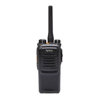
Hytera HD785 Service Manual (513 pages)
Brand:
Hytera
| Category:
Portable Radio
| Size: 17.75 MB
Table of Contents
Table of Contents
4
Documentation Information
11
1 Introduction
12
2 Product Controls
13
3 Baseband Section
16
Power Section
16
Diagram of Power Control
16
Radio On/Off
16
Figure 3-1 Diagram of Power Control
16
Figure 3-2 Diagram of Radio On/Off Control
16
Power Protection
17
Power Consumption Control
17
Control Section
17
OMAP5912 Dual-Core Processor
17
Figure 3-3 Diagram of OMAP5912
18
Figure 3-4 Diagram of Overall Scheme
18
External Memory
19
Figure 3-5 Diagram of External Memory
19
Clock
20
Figure 3-6 Diagram of Baseband Clock
20
Reset Signal
21
Spi
21
Mcbsp
21
Figure 3-7 Diagram of Reset Signal
21
Figure 3-8 Diagram of SPI Connection
21
Usb
22
Figure 3-9 Diagram of MCBSP Connection
22
Figure 3-10 Diagram of USB Interface
22
Uart
23
I2C
23
Figure 3-11 Diagram of UART Interface Connection
23
Figure 3-12 Diagram of I2C Connection
23
Microwire
24
Mcsi1
24
Audio Section
24
Audio Diagram
24
Figure 3-13 Diagram of MICROWIRE Connection
24
Figure 3-14 Diagram of MCSI1 Connection
24
Diagram of Signal Flow
25
Figure 3-15 Diagram of Audio Section
25
Audio Amplifier
26
Figure 3-16 Diagram of Audio Signal Flow
26
Troubleshooting Flow Chart
27
PCB Difference
28
4 GPS Circuit
29
Circuit Description
29
Figure 4-1 Diagram of GPS Circuit
29
Schematic Diagram
30
Parts List
30
Figure 4-2 Schematic Diagram
30
Troubleshooting Flow Chart
33
5 Tuning Description
34
6 Interface Definition
35
Table 6-1 Definition of 50-Pin Interface
37
Table 6-2 Definition of 30-Pin LCD Interface
37
Table 6-3 Definition of Channel Board Interface
38
Table 6-4 Definition of 20-Pin Option Board Interface
40
Table 6-5 Definition of 16-Pin Accessory Interface
40
Table 6-6 Definition of Accessory Identifiers
41
7 UHF1 (400-470Mhz) Information
42
Transmitter Circuit
42
RF Power Amplifier Circuit
42
Figure 7-1 Diagram of Transmitter Circuit
42
Low-Pass Filter Circuit
43
Auto Power Control Circuit
43
Receiver Circuit
43
Receiver Front-End
44
Figure 7-2 Diagram of Receiver Circuit
44
Receiver Back-End
45
Frequency Generation Unit (FGU)
45
Figure 7-3 Diagram of if Processor
45
Figure 7-4 Diagram of FGU
46
Working Principle of PLL
46
Two-Point Modulation
47
Working Principle of VCO
47
PCB View
48
Block Diagram
56
Schematic Diagram
59
Parts List
75
Troubleshooting Flow Chart
125
8 UHF2 (450-520Mhz) Information
131
Transmitter Circuit
131
RF Power Amplifier Circuit
131
Figure 8-1 Diagram of Transmitter Circuit
131
Low-Pass Filter Circuit
132
Auto Power Control Circuit
132
Receiver Circuit
132
Receiver Front-End
133
Figure 8-2 Diagram of Receiver Circuit
133
Receiver Back-End
134
Frequency Generation Unit (FGU)
134
Figure 8-3 Diagram of if Processor
134
Figure 8-4 Diagram of FGU
135
Working Principle of PLL
135
Working Principle of VCO
135
Two-Point Modulation
136
PCB View
137
Block Diagram
145
Schematic Diagram
148
Parts List
164
Troubleshooting Flow Chart
215
9 UHF3 (350-400Mhz) Information
221
Transmitter Circuit
221
RF Power Amplifier Circuit
221
Figure 9-1 Diagram of Transmitter Circuit
221
Low-Pass Filter Circuit
222
Auto Power Control Circuit
222
Receiver Circuit
222
Receiver Front-End
223
Figure 9-2 Diagram of Receiver Circuit
223
Receiver Back-End
224
Frequency Generation Unit (FGU)
224
Figure 9-3 Diagram of if Processor
224
Figure 9-4 Diagram of FGU
225
Working Principle of PLL
225
Working Principle of VCO
225
Two-Point Modulation
226
PCB View
227
Block Diagram
235
Schematic Diagram
238
Parts List
254
Troubleshooting Flow Chart
305
10 UHF5 (806-941Mhz) Information
311
Transmitter Circuit
311
RF Power Amplifier Circuit
311
Figure 10-1 Diagram of Transmitter Circuit
311
Low-Pass Filter Circuit
312
Auto Power Control Circuit
312
Receiver Circuit
312
Receiver Front-End
313
Figure 10-2 Diagram of Receiver Circuit
313
Receiver Back-End
314
Frequency Generation Unit (FGU)
314
Figure 10-3 Diagram of if Processor
314
Figure 10-4 Diagram of FGU
315
Working Principle of PLL
315
Working Principle of VCO
315
Two-Point Modulation
316
PCB View
317
Block Diagram
325
Schematic Diagram
328
Parts List
344
Troubleshooting Flow Chart
398
11 VHF (136-174Mhz) Information
406
Transmitter Circuit
406
RF Power Amplifier Circuit
406
Figure 11-1 Diagram of Transmitter Circuit
406
Low-Pass Filter Circuit
407
Auto Power Control Circuit
407
Receiver Circuit
407
Receiver Front-End
408
Figure 11-2 Diagram of Receiver Circuit
408
Receiver Back-End
409
Frequency Generation Unit (FGU)
409
Working Principle of PLL
410
Working Principle of VCO
410
Direct Modulation
411
PCB View
412
Block Diagram
420
Schematic Diagram
423
Parts List
439
Troubleshooting Flow Chart
492
12 Disassembly and Assembly
498
Disassembling the Chassis
498
Disassembling the TX and RX Units
498
Assembly
499
13 Exploded View
500
14 Packing Guide
506
15 Specifications
507
16 Appendix
510
Table 16-1 UHF1 Blind Spot
511
Table 16-2 UHF2 Blind Spot
511
Table 16-3 UHF3 Blind Spot
512
Table 16-5 VHF Blind Spot
512
Advertisement
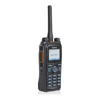
Hytera HD785 Service Manual (299 pages)
Brand:
Hytera
| Category:
Portable Radio
| Size: 8.03 MB
Table of Contents
Table of Contents
3
1 Revision History
5
2 Copyright Information
6
3 Disclaimer
7
4 Introduction
8
5 Product Controls
9
6 Baseband Section
11
Power Section
11
Control Section
12
External Memory
13
Audio Section
18
Troubleshooting Flow Chart
20
PCB Difference
21
7 GPS Circuit
22
Circuit Description
22
Schematic Diagram
23
Parts List
24
Troubleshooting Flow Chart
25
8 Tuning Description
26
9 Interface Definition
27
10 UHF1 (400-470Mhz) Information
31
Transmitter Circuit
31
Receiver Circuit
32
Frequency Generation Unit (FGU)
34
PCB View
36
Block Diagram
44
Schematic Diagram
47
Parts List
63
Troubleshooting Flow Chart
88
11 UHF2 (450-520Mhz) Information
94
Transmitter Circuit
94
Receiver Circuit
95
Frequency Generation Unit (FGU)
97
PCB View
99
Block Diagram
107
Schematic Diagram
110
Parts List
126
Troubleshooting Flow Chart
152
12 UHF3 (350-400Mhz) Information
158
Transmitter Circuit
158
Receiver Circuit
159
Frequency Generation Unit (FGU)
161
PCB View
163
Block Diagram
171
Schematic Diagram
174
Parts List
190
Troubleshooting Flow Chart
216
13 VHF (136-174Mhz) Information
222
Transmitter Circuit
222
Receiver Circuit
223
Frequency Generation Unit (FGU)
225
PCB View
227
Block Diagram
235
Schematic Diagram
238
Parts List
254
Troubleshooting Flow Chart
281
14 Disassembly and Assembly
287
15 Exploded View
289
16 Packing Guide
293
17 Specifications
294
18 Appendix
296
Hytera HD785 Service Manual (44 pages)
Brand:
Hytera
| Category:
Radio
| Size: 1.87 MB
Table of Contents
Contents
2
Copyright Information
3
Product Controls
5
Circuit Description
7
RF Section
7
Diagram of TX Circuit
7
Diagram of RX Circuit
8
Front-End Circuit
8
Rear-End Circuit
9
Diagram of if Processor
9
Frequency Generation Unit (FGU)
9
Diagram of FGU
10
Working Principle of PLL
10
Working Principle of VCO
10
Two-Point Modulation
11
Diagram of GPS Circuit
11
Baseband Section
11
Power Section
11
Diagram of Power Section
12
Diagram of Radio On/Off Control
12
Power Protection
13
Power Consumption Control
13
Control Section
13
OMAP5912 Dual-Core Processor
13
Diagram of Overall Scheme
14
Diagram of External Memory
14
Emifs
14
Emiff
15
Diagram of Baseband Clock
15
Input Clock
15
Output Clock
15
Diagram of Reset Signal
16
Diagram of SPI Connection
16
Mcbsp
16
Diagram of MCBSP Connection
17
Diagram of USB Interface
17
Uart
17
Diagram of UART Interface Connection
18
Diagram of IC2 Connection
18
Microwire
18
Diagram of Microwire Connection
19
Mcsi1
19
Audio Section
19
Audio Diagram
19
Diagram of Audio Section
20
Diagram of Signal Flow
20
Diagram of Audio Signal Flow
21
Audio Amplifier
21
Tuning Description
22
Port Definition
23
J1601: 50-Pin Interface
23
J311: 30-Pin LCD Interface
24
J2: 20-Pin Option Board Interface
24
16-Pin Accessory Interface
25
Definition of Accessory Identifiers
25
Troubleshooting Flow Chart
27
Control Circuit
27
RX Circuit
28
Description of Normal Situation
29
TX Circuit
30
Fgu
32
GPS Circuit
34
Disassembly and Assembly
35
Disassembling the Chassis
35
Disassembling the TX and RX Units
35
Precautions for Assembly
36
Exploded View
37
Packing Guide
39
Specifications
40
Appendix
42
Table of Blind Spots
42
Advertisement
Hytera HD785 Upgrade Manual (44 pages)
DMR Radio
Brand:
Hytera
| Category:
Radio
| Size: 0.85 MB
Table of Contents
Table of Contents
3
Documentation Information
4
R4.5
6
1 Important Tips before Upgrade
7
2 Before You Start
8
Firmware Version Check
8
Preparations
8
R5.5
9
3 Upgrade and Check
10
Entering the Download Mode
10
Pd78X/Pd88X/Pd98X/Hd785/Pd79X/Pd70X/Hd705/Pd71X
10
Md78X/Md65X
10
X1E/X1P/Pd60X/Pd66X/Pd68X
12
Starting Upgrade
12
After-Upgrade Check
16
Radio with Display
16
Radio Without Display
16
Applicable Model and Version
18
A6.01.05.006/S6.01
18
Advertisement
Related Products
Hytera HD785G
Hytera HP60X
Hytera HP6 0X
Hytera HM78 Series
Hytera HM686
Hytera HP56 Series
Hytera HP505
Hytera HM652GBTV
Hytera HM652GBTU1
Hytera HM785L
Hytera Categories
Portable Radio
Radio
Repeater
Two-Way Radio
Touch terminals
More Hytera Manuals
Login
Sign In
OR
Sign in with Facebook
Sign in with Google
Upload manual
Upload from disk
Upload from URL