Yamaha RX-V2500 Service Manual

Yamaha RX-V2500 Service Manual

Av receiver, av amplifier
Hide thumbs Also See for RX-V2500:
Table of Contents

Advertisement

RX-V2500/DSP-AX2500
This manual has been provided for the use of authorized YAMAHA Retailers and their service personnel.
It has been assumed that basic service procedures inherent to the industry, and more specifically YAMAHA Products, are already
known and understood by the users, and have therefore not been restated.
WARNING:
IMPORTANT:
The data provided is believed to be accurate and applicable to the unit(s) indicated on the cover. The research, engineering, and
service departments of YAMAHA are continually striving to improve YAMAHA products. Modifications are, therefore, inevitable
and specifications are subject to change without notice or obligation to retrofit. Should any discrepancy appear to exist, please
contact the distributor's Service Division.
WARNING:
IMPORTANT:
I CONTENTS
To Service Personnel .......................................... 2
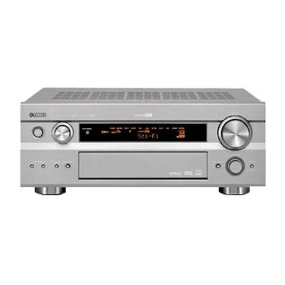
FRONT PANELS ........................................................ 3~4
REAR PANELS .......................................................... 4~7
Remote Control ...................................................... 7
SPECIFICATIONS / 参考仕様 .................................. 8~10
Internal View ......................................................... 11
DISASSEMBLY PROCEDURES / 分解手順 .......... 12~15
ファームウェアの書き込み ..................................... 16~17
SELF DIAGNOSIS FUNCTION (DIAG) /
自己診断機能(ダイアグ) ..................................... 18~42
1 0 0 9 2 2
AV RECEIVER/AV AMPLIFIER
IMPORTANT NOTICE
Failure to follow appropriate service and safety procedures when servicing this product may result in personal
injury, destruction of expensive components, and failure of the product to perform as specified. For these reasons,
we advise all YAMAHA product owners that any service required should be performed by an authorized
YAMAHA Retailer or the appointed service representative.
The presentation or sale of this manual to any individual or firm does not constitute authorization, certification or
recognition of any applicable technical capabilities, or establish a principle-agent relationship of any form.
Static discharges can destroy expensive components. Discharge any static electricity your body may have
accumulated by grounding yourself to the ground buss in the unit (heavy gauge black wires connect to this buss).
Turn the unit OFF during disassembly and part replacement. Recheck all work before you apply power to the unit.

SERVICE MANUAL

AMP ADJUSTMENT / アンプ部調整 ........................... 43
Display Data ........................................................... 44
Ic Data ................................................................. 45~48
Block Diagram ................................................. 49~50
Pin Connection Diagram .................................... 51
Printed Circuit Board .................................. 52~69
Schematic Diagram ........................................ 71~81
PARTS LIST ......................................................... 83~119
Remote Control .................................................. 120
P.O.Box 1, Hamamatsu, Japan
'04.11

Advertisement

Table of Contents
loading

Summary of Contents for Yamaha RX-V2500

  • Page 1: Service Manual

    This manual has been provided for the use of authorized YAMAHA Retailers and their service personnel. It has been assumed that basic service procedures inherent to the industry, and more specifically YAMAHA Products, are already known and understood by the users, and have therefore not been restated.
  • Page 2: To Service Personnel

    RX-V2500/DSP-AX2500 I TO SERVICE PERSONNEL AC LEAKAGE WALL EQUIPMENT TESTER OR 1. Critical Components Information OUTLET UNDER TEST EQUIVALENT Components having special characteristics are marked s and must be replaced with parts having specifications equal to those originally installed. 2. Leakage Current Measurement (For 120V Models Only)
  • Page 3: Front Panels

    RX-V2500/DSP-AX2500 I FRONT PANELS RX-V2500 (U, C, A models) RX-V2500 (R, T, K, L models) RX-V2500 (B, G models)
  • Page 4: Rear Panels

    RX-V2500/DSP-AX2500 DSP-AX2500 (J model) REAR PANELS RX-V2500 (U, C models) RX-V2500 (R model)
  • Page 5 RX-V2500/DSP-AX2500 RX-V2500 (T model) RX-V2500 (K model) RX-V2500 (A model)
  • Page 6 RX-V2500/DSP-AX2500 RX-V2500 (B model) RX-V2500 (G model) RX-V2500 (L model)
  • Page 7: Remote Control

    RX-V2500/DSP-AX2500 DSP-AX2500 (J model) I REMOTE CONTROL RX-V2500 (U, C, R, T, K, A, L models) RX-V2500 (B, G models) DSP-AX2500 (J model)
  • Page 8: Specifications

    RX-V2500/DSP-AX2500 I SPECIFICATIONS / 参考仕様 I Audio Section / オーディオ部 Minimum RMS Output Power (Power Amp. Section) / 定格出力 (パ Signal to Noise Ratio / 信号対雑音比 (IHF-A network) ワーアンプ部) (20 Hz to 20 kHz) PHONO (MM) (Input shorted) to SP OUT FRONT L/R U, C, R, T, K, L models (5mV) .......
  • Page 9 Dimensions / 寸法 (W x H x D) ..... 435 x 171 x 433.5 mm (17-1/8" x 6-3/4" x 17-1/16") Weight / 質量 RX-V2500 ........... 15.5 kg (34 lbs. 3 oz.) DSP-AX2500 ..........17.8 kg (39 lbs. 4 oz.) Finish / 仕上げ...
  • Page 10 RX-V2500/DSP-AX2500 • SET MENU TABLE / セットメニュー AUTO SETUP MAIN MENU PARAMETER SETUP AUTO FLAT / FRONT / [NATURAL] START PUSH + MANUAL SETUP MAIN MENU SUB MENU PARAMETER SETTING VALUE ([ ] INITIAL VALUE) MAIN MENU SUB MENU PARAMETER...
  • Page 11: Internal View

    RX-V2500/DSP-AX2500 I INTERNAL VIEW RX-V2500 (U, C, R, T, K, A, B, G, L models) 2 3 4 5 6 7 8 9 0 A B 1 POWER (5) P.C.B. 2 POWER (4) P.C.B. (R, L models only) 3 MAIN (1) P.C.B.
  • Page 12: Disassembly Procedures

    RX-V2500/DSP-AX2500 I DISASSEMBLY PROCEDURES / 分解手順 (番号順に部品を取り外してください。) (Remove parts in the order as numbered.) Disconnect the power cable from the AC outlet. AC電源コンセントから、電源コードを抜いてください。 1. トップカバーの外し方 1. Removal of Top Cover a. 1のネジ2本、2のネジ4本、3のネジ5本を外しま a. Remove 2 screws (1), 4 screws (2) and 5 screws (3).
  • Page 13 RX-V2500/DSP-AX2500 5. Removal of FUNCTION (3) P.C.B. 5. FUNCTION (3) P.C.B.の外し方 U, C, R, T, K, A, B, G, L models a. Remove 1 screw (B) and then remove the Support a. Bのネジ1本を外し、サポートトップを外します。 (Fig. Top. (Fig. 2) 2) b. Remove 1 screw (C).
  • Page 14 RX-V2500/DSP-AX2500 7. Removal of Fan 7. ファンの外し方 When checking the P.C.B.: P.C.B.チェックをする場合には a. Remove 4 push rivets (F) and then remove the Cover. a. Fのプッシュリベット4本を外し、カバーを外します。 ・ 本機の上にゴムシートと布を敷き、その上にP.C.B.を • Put the Rubber Sheet and a Cloth over the equipment. (Fig. 5) (Fig.
  • Page 15 RX-V2500/DSP-AX2500 When checking the Amp Unit: アンプユニットをチェックする場合には ・ アンプユニットはヒートシンクといっしょに、アート • Put the Amp Unit together with the heat sink upright ベースの上に立ててチェックします。 (Fig. C) on the art base and check them. (Fig. C) • Reconnect all cables (connectors) that have been ・...
  • Page 16: Updating Firmware

    RX-V2500/DSP-AX2500 I UPDATING FIRMWARE / ファームウェアの書き込み CONTROL P.C.B.のIC503をサービス部品 (X5934A00) に After replacing the IC503 on the CONTROL P.C.B. with the service part (X5934A00), update the firmware 交換した場合、下記の手順によりファームウェアの書き込 according to the following procedure. みを行ってください。 Equipment required 必要なツール ・ RS-232Cシリアルポート付きPC (OS: Windows 98/ •...
  • Page 17 RX-V2500/DSP-AX2500 3. 本機の電源をONします 3. Turn on the power to the unit. 4. To connect the line, click the CONNECT button or the 4. ラインに接続するためにCONNECTボタンまたはCOM メニューをクリックし、CONNECTをクリックします。 COM menu, then click the CONNECT. COM > CONNECT Menu After connecting, the "Connected" message is 接続された後、ステータスバーに...
  • Page 18 RX-V2500/DSP-AX2500 I SELF DIAGNOSIS FUNCTION (DIAG)/自己診断機能 (ダイアグ) ダイアグメニューは1 8 個あり、そのそれぞれにサブメ There are 18 DIAG menu items, each of which has sub- menu items. Listed in the table below are menu items and ニューがあります。下表はメニュー一覧です。 sub-menu items. No DIAG MENU SUB MENU DA601-YSS930 1.
  • Page 19 RX-V2500/DSP-AX2500 No DIAG MENU SUB MENU 12 AD DATA CHECK / FAN TEST 1. PS (protection) 2. DC (protection) / FAN OUT 3. TH 4. REC-OUT 5. PL 6. K0 / K1 (panel key) 7. FAN DRIVE TEST: HIGH (Fan test only applies to models with a fan. / ファン装備モデルに適用...
  • Page 20 RX-V2500/DSP-AX2500 • Starting DIAG ● ダイアグの起動 Press the “STANDBY/ON” key while simultaneously 本体の下図に示すキーを同時に押しながら “STANDBY/ pressing those two keys of the main unit as indicated in the ON” キーを押すと、ダイアグが起動します。 figure below. / 本体キー Keys of main unit Turn on the power while pressing these keys.
  • Page 21 RX-V2500/DSP-AX2500 • Display provided when DIAG started ● ダイアグ起動時の表示 The FL display of the main unit displays the protection 本体のFLディスプレイにプロテクション履歴情報とバー ジョン (英1文字) が表示され、数秒後にダイアグメニュー function history data and the version (1 alphabet) and the (No.1 DSP THROUGHのサブメニューYSS 0dB) になりま DIAG menu [sub-menu (YSS 0dB) of DIAG menu No.1 DSP THROUGH] a few seconds later.
  • Page 22 RX-V2500/DSP-AX2500 When there is a history of protection function due to abnormal voltage in the power supply section Version (1 alphabet) 電源部の電圧異常によるプロテク バージョン (英1文字) ション履歴がある場合 Voltage display in % 電圧の%表示 Cause: The voltage in the power supply section is 原因: 電源部の電圧が異常。...
  • Page 23 RX-V2500/DSP-AX2500 • History of protection function ● プロテクションの履歴 When the protection function has worked, its history is プロテクションが働いた場合、履歴をバックアップして stored in memory with a backup. Even if no abnormality 記憶しています。サービスのときに異常が認められなく is noted while servicing the unit, an abnormality which ても、バックアップが残っていれば、お客様のところで has occurred previously can be defined as long as the 起きた異常を区別できます。...
  • Page 24 RX-V2500/DSP-AX2500 • Functions in DIAG mode ● ダイアグ中の機能 In addition to the DIAG menu items, functions as listed ダイアグメニューの他に、以下の機能が動作します。 below are available. ・インプット切り換え、マルチチャンネルインプット • Input selection, Multi channel input ・センター、リア、リアセンター、サブウーファーレベル • Center/Rear/Rear center/Sub-woofer level adjustment 調整 • Muting ・ミューティング • Speaker relay A/B ・スピーカーリレーA/B...
  • Page 25 RX-V2500/DSP-AX2500 • Details of DIAG menu ● ダイアグメニュー詳細 With full-bit output specified in some modes, it is possible 一部のモードでフルビット指定することで、各チャンネル to execute 0dBFS output without head margin in each のヘッドマージンを廃して0dBFS出力することが可能で channel. す。 1. DA601-YSS930 1. DA601-YSS930 This function is for YSS930 only. Main DSP of YSS930 YSS930のみの動作です。FRONT出力にはYSS930の...
  • Page 26 RX-V2500/DSP-AX2500 2. BYPASS 2. BYPASS ANALOG BYPASS ANALOG BYPASS Reference data INPUT: DVD ANALOG SUBWOOFER OUTPUT: 50Hz, Others: 1kHz SPEAKER OUT SUBWOOFER Input level Volume FRONT CENTER SURROUND SURROUND BACK PRESENCE OUTPUT - ∞ - ∞ - ∞ - ∞...
  • Page 27 RX-V2500/DSP-AX2500 3. RAM THROUGH 3. RAM THROUGH Using the sub-menu, it is possible to select the full-bit サブメニューにより出力レベル0dB、フルビット出力が output at 0dB output level. 選択可能です。 RAM 0dB RAM 0dB Reference data INPUT: DVD ANALOG SUBWOOFER OUTPUT: 50Hz, Others: 1kHz SPEAKER OUT...
  • Page 28 RX-V2500/DSP-AX2500 4. PRO LOGIC / NEO6 4. PRO LOGIC / NEO6 PRO LOGIC I PRO LOGIC I Reference data INPUT: DVD ANALOG SUBWOOFER OUTPUT: 50Hz, Others: 1kHz SPEAKER OUT SUBWOOFER Input level Volume FRONT CENTER SURROUND SURROUND BACK PRESENCE OUTPUT - ∞...
  • Page 29 RX-V2500/DSP-AX2500 5. SPEAKERS SET 5. SPEAKERS SET The input signal is automatically identified in the order 入力は、dts→ DOLBY DIGITAL → AAC → PCM → ア of dts → DOLBY DIGITAL → AAC→ PCM → Analog. ナログの優先順で自動判別されます。 There are seven sub-menu items as follows. The サブメニューは以下の7つあります。...
  • Page 30 RX-V2500/DSP-AX2500 6. EXTERNAL INPUT 6. EXTERNAL INPUT It is possible to select the 6ch/8ch input and 6_/8_ by サブメニューにより、6ch/8ch入力および6Ω/8Ωが選択 using the SUB menu. 可能です。 6CH INPUT_6OHMS 6CH INPUT_6OHMS 6CH INPUT_8OHMS 6CH INPUT_8OHMS 8CH INPUT_6OHMS 8CH INPUT_6OHMS 8CH INPUT_8OHMS 8CH INPUT_8OHMS...
  • Page 31 RX-V2500/DSP-AX2500 8. EFFECT OFF / DISPLAY CHECK 8. EFFECT OFF / DISPLAY CHECK Use this program to check the FL display section and FL表示部と映像制御部のチェックプログラムです。 映 image control section. When checking the image 像制御部をチェックする場合には、モニター、コンポー ネントビデオケーブル、Sビデオケーブル、ビデオ用ピ control section, prepare a monitor, component video cable, S video cable and video pin cable and connect ンケーブルを準備し、接続します。...
  • Page 32 RX-V2500/DSP-AX2500 Check of the Video control circuit. (Monitor out) / 映像表示部のチェック(モニター出力) The image signal is output as follows. 映像信号は以下のように出力されます。 Initial display/Video conversion OFF INPUT OUTPUT 初期表示/ビデオコンバージョンOFF (D4 VIDEO JACK) (D4 VIDEO JACK) J model only J model only (D4ビデオ端子) (D4ビデオ端子)...
  • Page 33 RX-V2500/DSP-AX2500 9. MANUAL TEST 9. MANUAL TEST DSP内蔵のノイズ発生回路によって、サブメニューで指 The noise generator with a built-in DSP outputs the test 定したチャンネルへテストノイズを出力します。 noise through the channels specified by the sub-menu. LFE用のノイズ周波数は35∼250Hz、それ以外は中心周 The noise frequency for LFE is 35 to 250 Hz. Other than that, the center frequency is 800Hz.
  • Page 34 RX-V2500/DSP-AX2500 11. FACTORY PRESET 11. FACTORY PRESET This menu is used to reserve and inhibit initialization of バックアップ用RAM (音場プログラムのパラメーターや the back-up RAM. The signals are processed using セットメニュー内容等) の初期化を予約/禁止します。 信号処理はEFFECT OFFと同じです (ANALOG MAIN EFFECT OFF. (The L/R signal is output using ANALOG MAIN BYPASS.)
  • Page 35 RX-V2500/DSP-AX2500 12. AD DATA CHECK / FAN TEST 12. AD DATA CHECK / FAN TEST This menu is used to display the A/D conversion value 本体パネルキー、プロテクションなどを検出しているメ of the main CPU which detects panel keys of the main インCPUのA/D変換の値を、サブメニューで%表示しま す。信号処理は実行前の状態を維持します。 unit and protection functions in % using the sub-menu.
  • Page 36 RX-V2500/DSP-AX2500 POWER LIMIT (パワーリミッターの検出) POWER LIMIT (Power limiter detection) PL: Power limiter detection value PL: パワーリミッター検出の値 The voltage value of pin No. 135 of IC520 is displayed, IC520 135ピンの電圧値を5V/256を基準にして表示し ます。 using 5V/256 as standard. Based on the input voltage value of pin No.135 of IC520 135ピンの入力電圧値により、IC505の6ピン...
  • Page 37 RX-V2500/DSP-AX2500 13. V CONV STATUS 13. V CONV STATUS The data received from the video conversion IC ビデオコンバージョンIC (TA1270) からの受信データを (TA1270) is displayed. 表示します。 LOW BYTE DATA LOW BYTE DATA The status information of TA1270 is displayed in the TA1270のステータス情報を2進数で表示します。...
  • Page 38 RX-V2500/DSP-AX2500 14. IF STATUS 14. IF STATUS (Input function status) Using the sub-menu, the status data is displayed one サブメニュー操作により、以下のステータス情報を順次 after another in the hexadecimal notation. 16進数で表示します。信号処理は、本メニュー実行前 の状態を維持します。 During signal processing, the status before execution of this menu is maintained.
  • Page 39 RX-V2500/DSP-AX2500 <第5バイト>信号処理ステータス情報 <5th byte> Signal processing status information *2: With digital signals other than 32kHz, 44.1kHz and *2: 32kHz、44.1kHz、48kHz以外のデジタル信号の場 48kHz, through processing method is used for 合、再生可能な信号についてはスルー処理されます。 reproducible signals. bit7 MUTE request bit3 – bit6 Red dts flashing bit2 Through & bypass (*2) bit5 6.1/EX processing...
  • Page 40 RX-V2500/DSP-AX2500 15. DSP RAM CHECK 15. DSP RAM CHECK This menu is used to self-diagnose whether or not the YSS930と外付けRAMとのバス接続の正否を自己診断し bus connection for the YSS930 and the external RAM is ます。 信号処理は、このメニューを実行する前の状態を維持し made properly. During signal processing, the status before execution ます。...
  • Page 41 RX-V2500/DSP-AX2500 17. SOFT SW 17. SOFT SW This menu is used to switch the function settings on P.C.B.上の機能設定をソフト的に切り替えて、製品を動 P.C.B. through the software so as to activate the 作させる機能です。 プロテクション機能は、P.C.B.の設定に従います。AC product. The protection function follows the P.C.B. settings. 接続またはメーカープリセットで、P.C.B.の設定に初期 化されます。初期化後の各機能の表示は、P.C.B.上の設 When connected to AC or in the maker preset state, the 定によります。操作は、サブメニューを選んだ後、...
  • Page 42 RX-V2500/DSP-AX2500 18. マイコン情報 18. MICROPROCESSOR INFORMATION The version, checksum and the port specified by the サブメニューは9つあります。 microprocessor are displayed. The signal is processed プログラムのバージョン、チェックサム、マイコンの指 定ポートを表示します。 using EFFECT OFF. The checksum is obtained by adding the data at every 16 bits for each program area 信号はエフェクトOFFです。チェックサムは、プログラ...
  • Page 43 RX-V2500/DSP-AX2500 I AMP ADJUSTMENT / アンプ部調整 アンプユニットのアイドリング電流の確認 Confirmation of Idling Current of Amp ● 電源投入直後、R319 (MAIN Lch) 、R320 (MAIN REAR Unit Rch) 、R325 (CENTER) 、R326 (SURROUND • Right after power is turned on, confirm that the voltage Lch) 、R327 (SURROUND Rch) 、R321 MAIN (2) P.
  • Page 44: Display Data

    RX-V2500/DSP-AX2500 I DISPLAY DATA G V901 : 17-BT-23GNK (WD507500) G ANODE CONNECTION 14G~2G PATTERN AREA G PIN CONNECTION Pin No. Connection Pin No. Connection Note : 1) F1, F2 ..Filament 2) NP ..No pin 3) NC ..No connection 4) NX ..
  • Page 45 RX-V2500/DSP-AX2500 IC501 : M30805SGP (CONTROL P.C.B) I IC DATA 16bit µ-COM (Main CPU) IC501 : M30805SGP (CONTROL P.C.B) Port Name Terminal Name Function 16bit µ-COM (Main CPU) PowerOn Standby MCUSleep [AC OFF] TXDH TXD4 RESERVE (Unconnected) CLKH CLK4 RESERVE (Unconnected)
  • Page 46 RX-V2500/DSP-AX2500 IC501 : M30805SGP (CONTROL P.C.B) IC501 : M30805SGP (CONTROL P.C.B) 16bit µ-COM (Main CPU) 16bit µ-COM (Main CPU) Port Name Terminal Name Function Port Name Terminal Name Function PowerOn Standby MCUSleep [AC OFF] PowerOn Standby MCUSleep [AC OFF] SCKN...
  • Page 47 RX-V2500/DSP-AX2500 IC512: D601A003BPYP225 (DSP P.C.B) IC512: D601A003BPYP225 (DSP P.C.B) Decoder Decoder * No service part No. Name Function Digital Signal Processors avilable. 41 SCL0 I2C0 clock EMIF32 L2 Cache/ L1P Cache Memory ※ サービス部品として供給し Direct Mapped 42 SDA0 I2C0 data...
  • Page 48 RX-V2500/DSP-AX2500 IC512: D601A003BPYP225 (DSP P.C.B) IC512: D601A003BPYP225 (DSP P.C.B) Decoder Decoder No. Name Function No. Name Function 157 CVDD 1.2V power supply 99 EA17 For external memory, Address 17 (Unconnected) 158 VSS Ground 100 EA19 For external memory, Address 19 (Unconnected)
  • Page 49 RX-V2500/DSP-AX2500 I BLOCK DIAGRAM (1/2) • See page 71, 72 → SCHEMATIC DIAGRAM • See page 80, 81 → SCHEMATIC DIAGRAM IC532 IC524 (SP Current Detection) CONTROL IC532 Extended IC525 DIRSD0 Port DAFL IC506 Selector CPNTD 47,48 DAFR IC535 IC526...
  • Page 50 RX-V2500/DSP-AX2500 I BLOCK DIAGRAM (2/2) • See page 75 → SCHEMATIC DIAGRAM • See page 78, 79 → SCHEMATIC DIAGRAM • See page 78, 79 → SCHEMATIC DIAGRAM OPERATION INPUT INPUT IC710 IC701,702 IC606 Q709,712,713 IC716 V-AUX IC710 Q753 IC707...
  • Page 51 RX-V2500/DSP-AX2500 I PIN CONNECTION DIAGRAM • ICs • Diodes µPC29M33T-E1 RH5RE39AA PQ012FZ01ZP PQ03RD23 PQ09RF11 1N4002S MTZJ3.0A 1SS355 LM61CIZ NJM7805FA NJM79M05FA PQ025EZ5MZPH PQ05RD21 1SS133 MTZJ3.0B 1SS380 NJM7812FA NJM79M12FA RH5RE58AA Anode 1SS244 MTZJ33B MA8051-M Anode MTZJ4.7C MA8051-L MTZJ5.1B MA8056-M MTZJ6.8B MA8068-L Cathode MTZJ7.5C...
  • Page 52 RX-V2500/DSP-AX2500 I PRINTED CIRCUIT BOARD (Foil side) • Semiconductor Location Ref. No. Location D501 D509 IC501 DSP P.C.B. (Side A) Lead Solder Used CONTROL IC502 (CB511) IC504 IC505 POWER (3) IC506 (W127) IC507 INPUT (1) OPERATION (3) IC508 (W301) (CB905)
  • Page 53 RX-V2500/DSP-AX2500 I PRINTED CIRCUIT BOARD (Foil side) • Semiconductor Location Ref. No. Location D502 D503 D504 DSP P.C.B. (Side B) Lead Free Solder Used D508 D701 D702 D703 D704 D705 D706...
  • Page 54 RX-V2500/DSP-AX2500 I PRINTED CIRCUIT BOARD (Foil side) FUNCTION (3) FUNCTION (1) P.C.B. FUNCTION (1) P.C.B. (Side B) Lead Free Solder Used (CB523) (Side A) Lead Solder Used RS-232C FRONT /ICEV CEEV SURROUND DTEV PRE OUT DTEV3 CKEV SUB WOOFER SCKA...
  • Page 55 RX-V2500/DSP-AX2500 I PRINTED CIRCUIT BOARD (Foil side) FUNCTION (2) P.C.B. (Side A) Lead Solder Used FUNCTION (2) P.C.B. (Side B) Lead Free Solder Used FUNCTION (3) (CB533) RDATA RCLK /ICEV CEEV DTEV CKEV SDATA SCKA ATTF MTZ3 MTZ2 MTSW CBL/SAT...
  • Page 56 RX-V2500/DSP-AX2500 I PRINTED CIRCUIT BOARD (Foil side) • Semiconductor Location Ref. No. Location D508 D509 D510 FUNCTION (3) P.C.B. (Side A) Lead Solder Used IC541 Q515 Q516 Q517 Q547 INPUT (1) /VMT RCLK RCLK /Z2VMT RDATA SDAT FUNCION (2) (CB301)
  • Page 57 RX-V2500/DSP-AX2500 I PRINTED CIRCUIT BOARD (Foil side) • Semiconductor Location Ref. No. Location D504 Q542 Q548 FUNCTION (3) P.C.B. (Side B) Lead Free Solder Used...
  • Page 58 RX-V2500/DSP-AX2500 I PRINTED CIRCUIT BOARD (Foil side) FUNCTION (4) P.C.B. (Side A) Lead Solder Used FUNCTION (5) P.C.B. FUNCTION (6) P.C.B. (Side A) Lead Solder Used (Side A) Lead Solder Used +12R FUNCTION (2) FUNCTION (2) FUNCTION (2) INPUT (2)
  • Page 59 RX-V2500/DSP-AX2500 I PRINTED CIRCUIT BOARD (Foil side) • Semiconductor Location Ref. No. Location D901 D902 OPERATION (1) P.C.B. (Side A) D903 CONTROL D904 (CB508) D905 IC901 Q901 POWER (2) Q902 (CB125) Q903 Q904 Q905 Q908 Q909 Q910 Q913 INPUT PURE DIRECT...
  • Page 60 RX-V2500/DSP-AX2500 I PRINTED CIRCUIT BOARD (Foil side) • Semiconductor Location Ref. No. Location D906 D907 D908 OPERATION (2) P.C.B. (Side A) OPERATION (3) P.C.B. (Side A) IC902 IC903 IC904 Q911 Q912 CONTROL VOLUME CONTROL (W502) +5SPC OPERATION (4) (CB507) (W902B)
  • Page 61 RX-V2500/DSP-AX2500 I PRINTED CIRCUIT BOARD (Foil side) OPERATION (4) P.C.B. (Side A) OPERATION (5) P.C.B. (Side A) REC OUT MAIN (1) (W220) +5SPC OPERATION (3) (W902A) +5M2 PLMT PRIO TRG2 LIMIT TRG1 RM3+ +5M2 RM3- RM2+ THM1 RM2- THM2 OPERATION (4) P.C.B. (Side B) Lead Free Solder Used...
  • Page 62 RX-V2500/DSP-AX2500 I PRINTED CIRCUIT BOARD (Foil side) MAIN (1) P.C.B. (Side A) SURROUND / SURROUND BACK – – PRESENCE / ZONE 2 MAIN (2) P.C.B. (Side A) (W207A) MAIN (4) (W206A) SPA+ MAIN (3) SPA- SPB+ (CB216) SPB- SPE+ SPE-...
  • Page 63 RX-V2500/DSP-AX2500 I PRINTED CIRCUIT BOARD (Foil side) • Semiconductor Location Ref. No. Location D209 D210 D211 MAIN (3) P.C.B. (Side A) MAIN (5) P.C.B. (Side A) D212 D213 D216 D217 FRONT A/B CENTER D218 D219 – – – D220 D225...
  • Page 64 RX-V2500/DSP-AX2500 I PRINTED CIRCUIT BOARD (Foil side) • Semiconductor Location Ref. No. Location POWER (1) P.C.B. POWER (4) P.C.B. (Side A) OPERATION (5) (CB549) (Side A) R, L models only FUNCTION (1) (W501) Power Transformer Power Transformer D132 D133 D136...
  • Page 65 RX-V2500/DSP-AX2500 I PRINTED CIRCUIT BOARD (Foil side) • Semiconductor Location Ref. No. Location POWER (5) P.C.B. (Side A) POWER (6) P.C.B. (Side A) MAIN (3) FUNCTION (1) (W505) (W218) AC IN FAN- Flock FAN+ /RES PDET /LFAN D144 D145 D146...
  • Page 66 RX-V2500/DSP-AX2500 I PRINTED CIRCUIT BOARD (Foil side) INPUT (1) P.C.B. (Side A) Lead Solder Used INPUT (1) P.C.B. (Side B) Lead Free Solder Used CONTROL FUNCTION (5) FUNCTION (5) (CB515) (CB522) (CB521) FUNCTION (4) (CB548) ATTF SCKA SDTA RDATA RCLK (CB506) •...
  • Page 67 RX-V2500/DSP-AX2500 I PRINTED CIRCUIT BOARD (Foil side) INPUT (2) P.C.B. (Side A) Lead Solder Used INPUT (2) P.C.B. (Side B) Lead Free Solder Used VIDEO DVR/ VCR 1 VCR 2 ZONE2 MONITOR CBL/SAT /VMT /Z2VMT SDTN SCKN CMP0 CMP1 SEP_Y...
  • Page 68 RX-V2500/DSP-AX2500 I PRINTED CIRCUIT BOARD (Foil side) CONTROL P.C.B. (Side A) Lead Solder Used OPERATION (1) FUNCTION (3) (CB904) (CB505) (CB539) POWER (3) POWER (5) FUNCTION (3) (W124) (W1) (CB538) J model only DVD A D4 VIDEO KEY1B CBL/ +5SPC...
  • Page 69 RX-V2500/DSP-AX2500 I PRINTED CIRCUIT BOARD (Foil side) CONTROL P.C.B. (Side B) Lead Free Solder Used • Semiconductor Location Ref. No. Location Ref. No. Location Ref. No. Location Ref. No. Location Ref. No. Location Ref. No. Location Ref. No. Location Ref. No. Location Circuit No.
  • Page 70 RX-V2500/DSP-AX2500 MEMO MEMO...
  • Page 71 RX-V2500/DSP-AX2500 SCHEMATIC DIAGRAM (DSP 1/2) Page 75 from OPERATION(3) – V-AUX – CB905 Page 77 Page 80 IC510: SN74AHCT1G32DCKR from POWER(3)_W127 to CONTROL_CB511_23Pin 2-Input or Gate IC511: SN74AHCT08PWR Quad 2-Input And Gate REGULATOR IC513: SN74LV245APWR Octal Bus Transceiver with 3-state Outputs...
  • Page 72 RX-V2500/DSP-AX2500 SCHEMATIC DIAGRAM (DSP 2/2) Page 80 Page 78 to CONTROL (AUDIO)_CB502_19Pin to INPUT_W301 FRONT L IC516, 518: YSS930-SZ 11.7 NE5532DR MICROPROCESSOR INTERFACE PROGRAM COEFFICIENT ADDRESS NE5532DR CONTROL REGISTER 50 bit *1024 word 16 bit *1024 word 17 bit *256 word -12.0...
  • Page 73 RX-V2500/DSP-AX2500 SCHEMATIC DIAGRAM (FUNCTION 1/2) Page 74 Page 74 to FUNCTION (3) – C-F_CNCT – CB533 to FUNCTION (3) – C-F_CNCT – CB523 IC529: YAC523-EVR2 Digital Volume 0~95dB OUT1 – REF1B 0~+31.5dB REF1A VolA: 30kohm -11.9 11.7 0~95dB OUT2 –...
  • Page 74 RX-V2500/DSP-AX2500 SCHEMATIC DIAGRAM (FUNCTION 2/2) 11.8 11.8 ANALOG IN -6.1 FRONT L -12.0 CENTER SURROUND BACK L EZE2 EZE2 EZE2 PRESENCE L 11.7 -11.9 C683 UU23710 UR23722 UR23722 UR23722 UR23710 C676 10/16 22/16 22/16 22/16 10/16 C677 C678 C684 C675...
  • Page 75 RX-V2500/DSP-AX2500 SCHEMATIC DIAGRAM (OPERATION) Page 80 to CONTROL_CB508 IC901: M66003-0101FP FL Display Driver Display code CGROM SEG00 (8-bit x 60) (35 bit x 166) Segment SEG25 Code output write SEG26 circuit OPE (3) CGROM dot data SEG34 Serial data (35 bit x 16)
  • Page 76 RX-V2500/DSP-AX2500 SCHEMATIC DIAGRAM (MAIN) 61.4 61.4 61.0 -0.4 -1.0 -0.4 -0.4 -1.0 -1.0 -43.2 -43.5 -61.3 -61.3 -43.8 -44.3 MAIN (5) 61.4 61.4 61.0 -0.4 -1.0 -0.4 -0.4 -1.0 -1.0 -43.2 MAIN (1) -43.5 -43.8 -61.3 -61.3 -44.3 M_AMP. cir MAIN (2) 33.8...
  • Page 77 RX-V2500/DSP-AX2500 SCHEMATIC DIAGRAM (POWER) IC3: TC4013BP FF POWER (6) Dual D-type Flip Flop 44.0 RESET1 43.4 43.8 SET1 DATA1 43.2 44.2 43.5 43.2 43.2 -0.5 -0.5 CLOCK1 -0.6 -0.6 RESET2 SET2 DATA2 43.9 CLOCK2 44.0 43.4 43.3 44.1 43.3 44.2 43.5...
  • Page 78 RX-V2500/DSP-AX2500 SCHEMATIC DIAGRAM (INPUT 1/2) Page 72 Page 74 Page 80 Page 74 to DSP_CB506 to FUNCTION(3) – C-F_CNCT – CB530 to CONTROL_CB515 to FUNCTION(3) – C-F_CNCT – CB531 IC301, 304: NJU7312AM IC302: NJU7313AM Analog Function Switch Analog Function Switch...
  • Page 79 RX-V2500/DSP-AX2500 SCHEMATIC DIAGRAM (INPUT 2/2) Page 80 Page 80 to CONTROL_CB518_5Pin from FUNCTION (3) – C-F_CNCT – CB536_13Pin IC701 - 706: MM74HC4051SJX IC707, 710, 713: MM74HC4053SJX 8-Channel Analog Multiplexer Triple 2-Channel Analog Multiplexer IN/OUT IN/OUT OUT/IN Logic Binary to 1...
  • Page 80 RX-V2500/DSP-AX2500 SCHEMATIC DIAGRAM (CONTROL 1/2) ★ All voltages are measured with a 10MΩ/V DC electronic volt meter. ★ Components having special characteristics are marked s and must be replaced Page 72 with parts having specifications equal to those originally installed.
  • Page 81 RX-V2500/DSP-AX2500 SCHEMATIC DIAGRAM (CONTROL 2/2) Page 74 IC606, 607, 611: TC74HC4053AF(EL) from FUNCTION (6) – V-CNCT – Analog Multiplexer/Demultiplexer CB502_11Pin POINT A-2 Pin 3 of IC601 POINT A-3 Pin 12 of IC601 INHIBIT LEVEL BINARY TO 1-OF-8 CONVERTER DECODER WITH INHIBIT...
  • Page 82: Parts List

    RX-V2500/DSP-AX2500 PARTS LIST I ELECTRICAL PARTS I WARNING Components having special characteristics are marked s and must be replaced with parts having specifications equal to those originally installed. ●s印のある部分は、 安全確保部品を示 しています。 部品の交換が必要な場合、 パーツ リ ス トに記載されている部品を使用 して く ださい。 ●部品価格ランクは、 予告な く 変更するこ とがあ り ます。...
  • Page 83 RX-V2500/DSP-AX2500 P.C.B. DSP Schm Ref. PART NO. Description Remarks Markets 部 品 名 Rank WD650000 P.C.B. PCB DSP WD650100 P.C.B. UCRTKABGL PCB DSP CB502 VB858300 CN.BS.PIN コネクタベースポスト 01 CB503 VQ045300 CN.BS.PIN FFCコネクター CB505 VQ047400 CN.BS.PIN FFCコネクター CB506 LB919020 CN.BS.PIN ベース付ポスト C513 UR237220 C.EL 22uF ケミコン...
  • Page 84 RX-V2500/DSP-AX2500 P.C.B. DSP Schm Ref. PART NO. Description Remarks Markets 部 品 名 Rank C775 UA653390 C.MYLAR 3900pF マイラーコン C776 UA653390 C.MYLAR 3900pF マイラーコン C777 UA653390 C.MYLAR 3900pF マイラーコン C778 UA653390 C.MYLAR 3900pF マイラーコン C779 UA653390 C.MYLAR 3900pF マイラーコン C780 UA654680 C.MYLAR 0.068uF...
  • Page 85 RX-V2500/DSP-AX2500 P.C.B. DSP Schm Ref. PART NO. Description Remarks Markets 部 品 名 Rank D508 VT332900 DIODE 1SS355 ダイオード D509 VT332900 DIODE 1SS355 ダイオード D701 VV220700 DIODE.SHOT RB501V-40 ショットキーダイオード D702 VV220700 DIODE.SHOT RB501V-40 ショットキーダイオード D703 VV220700 DIODE.SHOT RB501V-40 ショットキーダイオード D704 VV220700 DIODE.SHOT RB501V-40 ショットキーダイオード...
  • Page 86 RX-V2500/DSP-AX2500 P.C.B. DSP & P.C.B. FUNCTION Schm Ref. PART NO. Description Remarks Markets 部 品 名 Rank U505 WB547900 CN.RHOT.SN 1P GP1FA513RZ 光ファイバ受信器 U506 WB547900 CN.RHOT.SN 1P GP1FA513RZ 光ファイバ受信器 XL501 V6931900 RESONATOR 24.576MHz DS0751SV 水晶発振器 WD650400 P.C.B. FUNCTION PCBファンクション WD650500 P.C.B. FUNCTION PCBファンクション...
  • Page 87 RX-V2500/DSP-AX2500 P.C.B. FUNCTION Schm Ref. PART NO. Description Remarks Markets 部 品 名 Rank C617 UR237100 C.EL 10uF UCABG ケミコン C618 UR237100 C.EL 10uF UCABG ケミコン C619 UR237100 C.EL 10uF UCABG ケミコン C620 UR267470 C.EL 47uF UCABG ケミコン C621 UR237100 C.EL 10uF UCABG ケミコン...
  • Page 88 RX-V2500/DSP-AX2500 P.C.B. FUNCTION Schm Ref. PART NO. Description Remarks Markets 部 品 名 Rank C677 UR237220 C.EL 22uF UCRTKAL ケミコン C678 UR237100 C.EL 10uF ケミコン C678 UR237220 C.EL 22uF UCRTKAL ケミコン C679 UR237220 C.EL 22uF ケミコン C680 UR237220 C.EL 22uF ケミコン C683 UR237100 C.EL...
  • Page 89 RX-V2500/DSP-AX2500 P.C.B. FUNCTION Schm Ref. PART NO. Description Remarks Markets 部 品 名 Rank PJ509 WD498400 JACK.PIN RJ-1073*10-0351A UCRTKABGL ピンジャック 4P PJ510 WD498800 JACK.PIN RJ-1073*87-0551A ピンジャック 4P PJ510 WD498700 JACK.PIN RJ-1073*87-0351A UCRTKABGL ピンジャック 4P PN501 V9637500 PIN L=70 #18 スタイルピン PN508 V9637500 PIN L=70 #18 スタイルピン...
  • Page 90 RX-V2500/DSP-AX2500 P.C.B. FUNCTION & P.C.B. OPERATION Schm Ref. PART NO. Description Remarks Markets 部 品 名 Rank R803 HF354470 R.CAR 47Ω 1/2W カーボン抵抗 R804 HF354470 R.CAR 47Ω 1/2W カーボン抵抗 R805 HF354470 R.CAR 47Ω 1/2W カーボン抵抗 R806 HF354470 R.CAR 47Ω 1/2W カーボン抵抗 ST501 V4040500 SCR.TERM スクリュー/ターミナル...
  • Page 91 RX-V2500/DSP-AX2500 P.C.B. OPERATION Schm Ref. PART NO. Description Remarks Markets 部 品 名 Rank IC904 XF291A00 IC uPC4570G2 IC JK901 V9408200 JACK.PHONE MSJ-064-05B GR ホーンジャック JK902 V2589500 CN ミニDINコネクタ JK903 VJ726800 JACK.MNI モノラルミニジャック 01 PJ901 V6222800 JACK.PIN ピンジャック PN502 V9637500 PIN L=70 #18 スタイルピン...
  • Page 92 RX-V2500/DSP-AX2500 P.C.B. OPERATION & P.C.B. MAIN Schm Ref. PART NO. Description Remarks Markets 部 品 名 Rank SW924 V4757100 SW.TACT EVQ11A タクトSW U901 V8210200 L.DTCT GP1UD271XK リモコン受光ユニット 03 U902 V7680700 CN.PHOT.SN 1P GP1FA512RZ 光ファイバ受信器 V901 WD507500 FL.DSPLY 17-BT-23GNK 螢光表示管 V6007000 SHEET シート/FL...
  • Page 93 RX-V2500/DSP-AX2500 P.C.B. MAIN Schm Ref. PART NO. Description Remarks Markets 部 品 名 Rank C259 UA654470 C.MYLAR 0.047uF マイラーコン C260 UA654470 C.MYLAR 0.047uF マイラーコン C261 VR325300 C.MYLAR 0.047uF 100V JKBGL マイラーコン C261 UA654470 C.MYLAR 0.047uF UCRTA マイラーコン C262 VR325300 C.MYLAR 0.047uF 100V JKBGL マイラーコン...
  • Page 94 RX-V2500/DSP-AX2500 P.C.B. MAIN Schm Ref. PART NO. Description Remarks Markets 部 品 名 Rank D216 WA180300 DIODE 1SS244 ダイオード D217 WA180300 DIODE 1SS244 ダイオード D218 WA180300 DIODE 1SS244 ダイオード D219 WA180300 DIODE 1SS244 ダイオード D220 WA180300 DIODE 1SS244 ダイオード D221 WA180300 DIODE 1SS244 ダイオード...
  • Page 95 RX-V2500/DSP-AX2500 P.C.B. MAIN Schm Ref. PART NO. Description Remarks Markets 部 品 名 Rank s Q225C iX632620 TR 2SC4793 O,Y トランジスタ * s Q226 WD281200 TR.PAIR 2SA2151/C6011 OPY JKBGL ペアトランジスタ s Q226A iX606460 TR 2SA1492 O,P,Y UCRTA トランジスタ s Q226C iX606470 TR...
  • Page 96 RX-V2500/DSP-AX2500 P.C.B. MAIN Schm Ref. PART NO. Description Remarks Markets 部 品 名 Rank s R220 HV753100 R.CAR.FP 1Ω 1/4W 不燃化カーボン抵抗 s R222 HV753100 R.CAR.FP 1Ω 1/4W 不燃化カーボン抵抗 R263 V3946100 R.MTL.OXD 2.7KΩ 1/2W 酸化金属被膜抵抗 s R264 V3945100 R.MTL.OXD 390Ω 1/2W 酸化金属被膜抵抗 R265 V3945500 R.MTL.OXD...
  • Page 97 RX-V2500/DSP-AX2500 P.C.B. MAIN Schm Ref. PART NO. Description Remarks Markets 部 品 名 Rank s R315 HV753470 R.CAR.FP 4.7Ω 1/4W 不燃化カーボン抵抗 s R316 HV753470 R.CAR.FP 4.7Ω 1/4W 不燃化カーボン抵抗 s R317 HV753470 R.CAR.FP 4.7Ω 1/4W 不燃化カーボン抵抗 s R318 HV753470 R.CAR.FP 4.7Ω 1/4W 不燃化カーボン抵抗...
  • Page 98 RX-V2500/DSP-AX2500 P.C.B. POWER Schm Ref. PART NO. Description Remarks Markets 部 品 名 Rank WD648200 P.C.B. POWER PCB パワー WD648300 P.C.B. POWER PCB パワー WD648400 P.C.B. POWER PCB パワー WD648500 P.C.B. POWER PCB パワー WD648600 P.C.B. POWER PCB パワー WD648700 P.C.B. POWER PCB パワー WD648800 P.C.B. POWER PCB パワー...
  • Page 99 RX-V2500/DSP-AX2500 P.C.B. POWER Schm Ref. PART NO. Description Remarks Markets 部 品 名 Rank V9415100 C.EL 10uF ケミコン UR237100 C.EL 10uF UCRTKAL ケミコン UU266470 C.EL 4.7uF ケミコン UR237100 C.EL 10uF UCRTKAL ケミコン UU266470 C.EL 4.7uF ケミコン UR237100 C.EL 10uF UCRTKAL ケミコン V9415100 C.EL 10uF ケミコン...
  • Page 100 RX-V2500/DSP-AX2500 P.C.B. POWER Schm Ref. PART NO. Description Remarks Markets 部 品 名 Rank UA652220 C.MYLAR 220pF マイラーコン UR267100 C.EL 10uF ケミコン UR297220 C.EL 22uF 100V ケミコン UR297220 C.EL 22uF 100V ケミコン UR267470 C.EL 47uF ケミコン UR267470 C.EL 47uF ケミコン UA653100 C.MYLAR 1000pF マイラーコン...
  • Page 101 RX-V2500/DSP-AX2500 P.C.B. POWER Schm Ref. PART NO. Description Remarks Markets 部 品 名 Rank C203 VF467000 C.CE.TUBLR 1000pF UCABG 円筒セラコン C204 VF467000 C.CE.TUBLR 1000pF UCABG 円筒セラコン C205 VF467000 C.CE.TUBLR 1000pF UCABG 円筒セラコン C206 VF467000 C.CE.TUBLR 1000pF UCABG 円筒セラコン C207 VF467300 C.CE.TUBLR 0.01uF UCABG 円筒セラコン...
  • Page 102 RX-V2500/DSP-AX2500 P.C.B. POWER Schm Ref. PART NO. Description Remarks Markets 部 品 名 Rank s IC3 iG001180 IC TC4013BP FF ロジックIC s IC121 XJ607A00 IC NJM7805FA 5V IC s IC123 XJ608A00 IC NJM7812FA IC s IC124 XD343A00 IC NJM79M12FA IC s IC126 XE436A00 IC NJM79M05FA IC...
  • Page 103 RX-V2500/DSP-AX2500 P.C.B. POWER Schm Ref. PART NO. Description Remarks Markets 部 品 名 Rank VP883100 TR 2SC1890A D,E トランジスタ VP883100 TR 2SC1890A D,E トランジスタ s Q62 VC938500 TR 2SC3852 トランジスタ s Q63 VC614000 TR 2SB1274 Q,R,S トランジスタ s Q64 V3966800 TR 2SA949 O,Y トランジスタ...
  • Page 104 RX-V2500/DSP-AX2500 P.C.B. POWER Schm Ref. PART NO. Description Remarks Markets 部 品 名 Rank HF355470 R.CAR 470Ω 1/2W カーボン抵抗 R101 HF357470 R.CAR 47KΩ 1/2W カーボン抵抗 R102 HF357470 R.CAR 47KΩ 1/2W カーボン抵抗 R105 HF357470 R.CAR 47KΩ 1/2W カーボン抵抗 R138 HF353220 R.CAR 2.2Ω 1/2W カーボン抵抗...
  • Page 105 RX-V2500/DSP-AX2500 P.C.B. INPUT Schm Ref. PART NO. Description Remarks Markets 部 品 名 Rank WD651600 P.C.B. INPUT PCB インプット WD651700 P.C.B. INPUT PCB インプット WD651800 P.C.B. INPUT RTKL PCB インプット WD651900 P.C.B. INPUT PCB インプット CB301 V8875300 CN.JE 13P SE JEコネクタープラグ 01 CB302 VQ963300 CN.BS.PIN ウエハー...
  • Page 106 RX-V2500/DSP-AX2500 P.C.B. INPUT Schm Ref. PART NO. Description Remarks Markets 部 品 名 Rank C371 UR237100 C.EL 10uF ケミコン C372 UR237100 C.EL 10uF ケミコン C375 UR237100 C.EL 10uF ケミコン C376 UR237100 C.EL 10uF ケミコン C377 UR238100 C.EL 100uF ケミコン C378 UR238100 C.EL 100uF ケミコン...
  • Page 107 RX-V2500/DSP-AX2500 P.C.B. INPUT Schm Ref. PART NO. Description Remarks Markets 部 品 名 Rank IC312 X3505A00 IC NJM2068MD-TE2 アンプIC SOP IC314 X3505A00 IC NJM2068MD-TE2 アンプIC SOP IC701 XY550A00 IC MM74HC4051SJX ロジックICSOP IC702 XY550A00 IC MM74HC4051SJX ロジックICSOP IC703 XY550A00 IC MM74HC4051SJX ロジックICSOP IC704 XY550A00 IC MM74HC4051SJX ロジックICSOP...
  • Page 108 RX-V2500/DSP-AX2500 P.C.B. INPUT & P.C.B. CONTROL Schm Ref. PART NO. Description Remarks Markets 部 品 名 Rank R795 HV755470 R.CAR.FP 470Ω 1/4W 不燃化カーボン抵抗 R810 HV753100 R.CAR.FP 1Ω 1/4W 不燃化カーボン抵抗 R811 HV753100 R.CAR.FP 1Ω 1/4W 不燃化カーボン抵抗 R818 HV753220 R.CAR.FP 2.2Ω 1/4W 不燃化カーボン抵抗 R824 HV755470 R.CAR.FP...
  • Page 109 RX-V2500/DSP-AX2500 P.C.B. CONTROL Schm Ref. PART NO. Description Remarks Markets 部 品 名 Rank C570 UR238100 C.EL 100uF ケミコン C586 UR238100 C.EL 100uF ケミコン C592 UR237470 C.EL 47uF ケミコン C626 UR268100 C.EL 100uF ケミコン C626 UR268330 C.EL 330uF UCRTKAL ケミコン C769 UR266100 C.EL ケミコン...
  • Page 110 RX-V2500/DSP-AX2500 P.C.B. CONTROL Schm Ref. PART NO. Description Remarks Markets 部 品 名 Rank D508 VU992600 DIODE.ZENR MA8051-M 5.1V ツェナーダイオード D509 VT332900 DIODE 1SS355 ダイオード D510 VT332900 DIODE 1SS355 ダイオード D511 VV833200 DIODE 1SS380 ダイオード D512 VT332900 DIODE 1SS355 ダイオード D513 VT332900 DIODE 1SS355 ダイオード...
  • Page 111 RX-V2500/DSP-AX2500 P.C.B. CONTROL Schm Ref. PART NO. Description Remarks Markets 部 品 名 Rank IC573 X4536A00 IC SN74AHCT126PW ロジックIC IC601 X4347A00 IC TA1270BF IC アナログ IC602 X4346A00 IC TA8772AN RTABGL IC アナログ IC603 X4349A00 IC TC90A49F IC デジタル IC604 X5611A00 IC BA7071F IC SOP IC606 XY879A00 IC TC74HC4053AF(EL) ロジックIC SOP...
  • Page 112 RX-V2500/DSP-AX2500 P.C.B. CONTROL Schm Ref. PART NO. Description Remarks Markets 部 品 名 Rank Q756 VV556500 TR 2SA1037K Q,R,S トランジスタ Q757 VV556400 TR 2SC2412K Q,R,S トランジスタ Q758 VV556400 TR 2SC2412K Q,R,S トランジスタ Q759 VV556400 TR 2SC2412K Q,R,S トランジスタ Q760 VV556500 TR 2SA1037K Q,R,S トランジスタ...
  • Page 113 RX-V2500/DSP-AX2500 Chip Parts Schm Ref. PART NO. Description Remarks Markets 部 品 名 Rank US044220 C.CE.M.CHP 0.022uF チップセラコン US060500 C.CE.CHP チップセラコン US060800 C.CE.CHP チップセラコン US061100 C.CE.M.CHP 10pF チップセラコン US061120 C.CE.CHP 12pF チップセラ(CH) US061150 C.CE.CHP 15pF チップセラコン US061180 C.CE.CHP 18pF チップセラコン US061220 C.CE.M.CHP 22pF チップセラコン...
  • Page 114 RX-V2500/DSP-AX2500 Parts List for Carbon Resistors Chip Parts Schm Value 1/4W Type Part No. 1/6W Type Part No. Value 1/4W Type Part No. 1/6W Type Part No. Ref. PART NO. Description Remarks Markets 部 品 名 Rank 1.0 Ω 3100 3100 10 kΩ...
  • Page 115 RX-V2500/DSP-AX2500 I EXPLODED VIEW R, L models J model 7 (4) 200-1 U, C, A, B, G models U, C, R, T, L, J models R, L models J, R, T, K, L models 7 (7) U, C, A, B,...
  • Page 116: Mechanical Parts

    RX-V2500/DSP-AX2500 I MECHANICAL PARTS Schm Schm Ref. PART NO. Description Remarks Markets 部 品 名 Rank Ref. PART NO. Description Remarks Markets 部 品 名 Rank WD655000 P.C.B. ASS'Y OPERATION JRTKL PCB オペレーション WC051600 D56/H21 GD,BL レッグ WD655100 P.C.B. ASS'Y OPERATION PCB オペレーション V0042500 D60xH21 RTKL レッグ...
  • Page 117 RX-V2500/DSP-AX2500 I FRONT PANEL & SUB CHASSIS UNIT Schm Ref. PART NO. Description Remarks Markets 部 品 名 Rank 2-52 WD429100 FRONT PANEL フロントパネル WD428600 FRONT PANEL RTKL フロントパネル 2-52 2-52 WD429000 FRONT PANEL フロントパネル 2-15 WD428500 FRONT PANEL UCRA フロントパネル WD428900 FRONT PANEL フロントパネル...
  • Page 118 RX-V2500/DSP-AX2500 I AMP UNIT Schm Ref. PART NO. Description Remarks Markets 部 品 名 Rank * s 3-1 WD654500 P.C.B. ASS'Y MAIN PCB メイン * s 3-1 WD654600 P.C.B. ASS'Y MAIN PCB メイン * s 3-1 WD654700 P.C.B. ASS'Y MAIN PCB メイン * s 3-1 WD654800 P.C.B.
  • Page 119 RX-V2500/DSP-AX2500 I REMOTE CONTROL RAV352, RAV353 RAV352 RAV353 (U, C, R, T, K, A, L, J models) (B, G models) AMP Library AMP Library AMP Library : AMP1Z AMP Library : AMP2Z Label AMP1 AMP2 MAIN ZONE2 ZONE3 SYSTM MAIN...

This manual is also suitable for:

Dsp-ax2500

Table of Contents