Table of Contents
Advertisement
QQ
3 7 63 1515 0
TE
L 13942296513
CONTENTS
TO SERVICE PERSONNEL ........................................... 1
REMOTE CONTROL PANELS ....................................... 1
REAR PANELS ............................................................... 2
SPECIFICATIONS ....................................................... 3~4
INTERNAL VIEW ............................................................ 5
DISASSEMBLY PROCEDURES .................................... 5
SELF DIAGNOSIS FUNCTION ................................ 6~17
www
FACTORY PRESET ...................................................... 18
.
1 0 0 7 1 2
http://www.xiaoyu163.com
DSP-A5
This manual has been provided for the use of authorized YAMAHA Retailers and their service personnel.
It has been assumed that basic service procedures inherent to the industry, and more specifically YAMAHA
Products, are already known and understood by the users, and have therefore not been restated.
WARNING:
IMPORTANT:
The data provided is believed to be accurate and applicable to the unit(s) indicated on the cover. The research,
engineering, and service departments of YAMAHA are continually striving to improve YAMAHA products.
Modifications are, therefore, inevitable and specifications are subject to change without notice or obligation
to retrofit. Should any discrepancy appear to exist, please contact the distributor's Service Division.
WARNING:
IMPORTANT:
x
u163
http://www.xiaoyu163.com
2 9
8
AV AMPLIFIER
SERVICE MANUAL
IMPORTANT NOTICE
Q Q
3
6 7
1 3
1 5
Failure to follow appropriate service and safety procedures when servicing this product
may result in personal injury, destruction of expensive components, and failure of the
product to perform as specified. For these reasons, we advise all YAMAHA product
owners that any service required should be performed by an authorized YAMAHA
Retailer or the appointed service representative.
The presentation or sale of this manual to any individual of firm does not constitute
authorization, certification or recognition of any applicable technical capabilities,
or establish a principle-agent relationship of any form.
Static discharges can destroy expensive components. Discharge any static electricity
your body may have accumulated by grounding yourself to the ground buss in the unit
(heavy gauge black wires connect to this buss).
Turn the unit OFF during disassembly and part replacement. Recheck all work before
you apply power to the unit.
AMP ADJUSTMENT ..................................................... 19
IC DATA .................................................................. 20~28
DISPLAY DATA ........................................................... 29
BLOCK DIAGRAM .................................................. 30~31
PRINTED CIRCUIT BOARD ................................... 32~47
SCHEMATIC DIAGRAM ......................................... 48~53
PARTS LIST ............................................................ 54~69
co
.
9 4
2 8
0 5
8
2 9
9 4
2 8
m
9 9
9 9
Advertisement
Table of Contents

Related Manuals for Yamaha DSP-A5


Summary of Contents for Yamaha DSP-A5
-
Page 1: Table Of Contents
SERVICE MANUAL IMPORTANT NOTICE This manual has been provided for the use of authorized YAMAHA Retailers and their service personnel. It has been assumed that basic service procedures inherent to the industry, and more specifically YAMAHA Products, are already known and understood by the users, and have therefore not been restated. -
Page 2: To Service Personnel
DSP-A5 3 7 63 1515 0 I TO SERVICE PERSONNEL 1. Critical Components information Components having special characteristics are marked and must be replaced with parts having specifications equal to those originally AC LEAKAGE installed. WALL EQUIPMENT TESTER OR 2. -
Page 3: Rear Panels
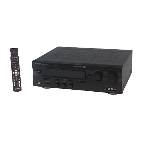
DSP-A5 3 7 63 1515 0 I REAR PANELS M R model M T model L 13942296513 M B model M G model u163 http://www.xiaoyu163.com... -
Page 4: Specifications
DSP-A5 3 7 63 1515 0 I SPECIFICATIONS IAUDIO SECTION Residual Noise(IHF-A Network) MAIN L/R, SP OUT 150µV Minimum RMS Output Power Per Channel Channel Separation(Vol. –30dB, EFFECT OFF) (Power Amp. Section) PHONO, Input shorted, 1kHz/10kHz 60dB/55dB MAIN L/R, REAR L/R CD etc, Input 5.1kΩ... - Page 5 DSP-A5 3 7 63 1515 0 G DIMENSIONS WARNING Do not change the IMPEDANCE SELECTOR switch setting while the power to this unit is on, otherwise this unit may be damaged. IMPEDANCE SELECTOR Manufactured under license from Dolby Laboratories.
-
Page 6: Internal View
DSP-A5 3 7 63 1515 0 I INTERNAL VIEW 1 POWER TRANSFORMER 2 P.C.B. POWER (2) 3 P.C.B. POWER (7) (B,G models only) 4 P.C.B. MAIN (3) 5 P.C.B. POWER (6) (R,T models only) 6 P.C.B. MAIN (4) 7 P.C.B. POWER (4) (R,T models only) 8 P.C.B. -
Page 7: Self Diagnosis Function
SELF DIAGNOSIS FUNCTION 1. PURPOSE AND OPERATION The DSP-A5 has a Self Diagnosis Function to locate a faulty part, if any, by inspecting and taking measurements. There are 12 main items in the diagnostic menu and have sub-menu items as listed below. - Page 8 DSP-A5 3 7 63 1515 0 2. BEGINNING AND CANCELLATION (1) Starting up the function and the display After starting up, main menu No.1 is selected. A. How to start diagnostic program Using the front panel keys of the main unit Plug in the AC power cord.
- Page 9 DSP-A5 3 7 63 1515 0 G FL display at start-up of diagnostic program When the diagnostic program has started, the check sum of the main microcomputer or the protection history (*1) is displayed. If the protection function has been activated in the past, the type and voltage value are displayed. After a few seconds the diagnosis function menu will appear.
- Page 10 DSP-A5 3 7 63 1515 0 3. OPERATION AND DISPLAY WHEN STARTING DIAGNOSIS FUNCTION (1) Selection of diagnostic menu The diagnostic menu and the sub-menu can be selected by using the front panel keys of the main unit or the remote control unit.
- Page 11 DSP-A5 3 7 63 1515 0 4. CONTENTS OF DIAGNOSIS FUNCTION This section describes the contents of the Self Diagnosis Function in detail. No.1 ANALOG THROUGH The input is fixed to analog (A/D). There are two sub-menus. 1 MA I N B Y P A S S 1.
- Page 12 DSP-A5 3 7 63 1515 0 No.2 DSP THROUGH The input is automatically discriminated by signal detection and switched with priorities Coaxial>Optical>Analog. There are the following three sub-menus. 2 Y S S + S R AM M 1. YSS+SRAM The L/R signals are output without being processed to the MAIN L/R through the AC3D2av.
- Page 13 DSP-A5 3 7 63 1515 0 No.3 AC-3/DTS THROUGH The input is digital signal only. AC-3 (DOLBY DIGITAL) or DTS Digital Surround decoding operation is executed, according to the input source. bit 1 bit 7 3 S T : 1 0 0 0 1 0 0 1 1.
- Page 14 DSP-A5 3 7 63 1515 0 No.5 SPEAKERS SET The input is automatically discriminated by signal detection and switched with priorities Coaxial>Optical>Analog. The L/R signals are output to channels specified by the sub-menu without being processed. There are the following nine sub-menus items. Signal routes of the sub-menu 1-4 are the same as EFFECT OFF.
- Page 15 DSP-A5 3 7 63 1515 0 No.6 DISPLAY CHECK Check program for FL display. The display status will change as follows with sub-menu operation. signal route is the same as "2. EFFECT OFF" of "No. 4 PRO LOGIC". 6 V F D C H C K...
- Page 16 DSP-A5 3 7 63 1515 0 No.9 AD DATA CHECK The A/D conversion values of the microcomputer which detects key scan port, protection detection port, etc. are displayed in % (100%:5V). Signal route is the same as "2. EFFECT OFF" of "No. 4 PRO LOGIC".
- Page 17 DSP-A5 3 7 63 1515 0 No.10 STATUS INFORMATION FROM DSP The status data from the DSP block is sequentially displayed in a hexadecimal number. Signal route is the same as "2. EFFECT OFF" of "No. 4 PRO LOGIC".
- Page 18 Version Check sum R X - V A B G L The model type and the destination are displayed. L 13942296513 RX-V: Model type. DSP-A= DSP-A5 Model type Destination RX-V = RX-V596, HTR-5250 RDS = RX-V596RDS ABGL: Destination. = J model...
-
Page 19: Factory Preset
DSP-A5 3 7 63 1515 0 I FACTORY PRESET All of the system settings are initially set from the factory as follows. INPUT SELECTOR EFFECT LEVEL INPUT FACTORY PRESET PROGRAM EFFECT CHANNEL PRESET VALUE PHONO CONCERT HALL CENTER 0 dB... -
Page 20: Ao Y
DSP-A5 3 7 63 1515 0 I AMP ADJUSTMENT Confirmation of Idling Current of Main Amplifier • Right after power is turned on, confirm that the voltage across the terminals of R688(Main Lch),R690(Main Rch), R692(Center), R694(Rear Lch), R696(Rear Rch) are between 0.1mV and 10.0mV. -
Page 21: Ic Data
DSP-A5 3 7 63 1515 0 I IC DATA IC501 : M30217MA-A203FP 16-bit Microcomputer P67/FL07 P24/FL36 P66/FL06 P25/FL37 P65/FL05 P26/FL38 P64/FL04 P27/FL39 P63/FL03 P30/FL40 P62/FL02 P31/FL41 P61/FL01 P32/FL42 P60/FL00 P33/FL43 P34/FL44 P107/AN7 P35/FL45 TOP VIEW P106/AN6 P36/FL46 P105/AN5 P37/FL47... - Page 22 DSP-A5 3 7 63 1515 0 IC501 : M30217MA-A203FP 16-bit Microcomputer Port Function Port Function Name Name For Input O Serial Clock output 31 P47/FL55 F-CE O Chip enable output selector Tuner, flash µ-COM O Serial Data output 32 P46/FL54...
- Page 23 DSP-A5 3 7 63 1515 0 IC501 : M30217MA-A203FP 16-bit Microcomputer Port Function Port Function Name Name 67 P05/FL21 O Segment 1 for FL display 85 P63/FL03 O Segment 19 for FL display 68 P04/FL20 O Segment 2 for FL display...
- Page 24 DSP-A5 3 7 63 1515 0 IC3 : YSD917 (DIR5) Digital Format Interface Receiver AVDD STANDARD SDMCK CLOCK AVSS CLOCK OUTPUT GENERATION SDWCK SYSTEM CLOCK SDBCK GENERATION SELECTION DDIN DDIN SYNC TEST FS128 OUTPUT /LOCK SELECTION TOP VIEW DATA BUS...
- Page 25 DSP-A5 3 7 63 1515 0 IC4 : YSS918D-F (AC3D2av) DSP + AC-3(Dolby Digital)/ Pro Logic/ DTS Digital Surround Decoder PVSS SDWCK0 SDWCK1 SDBCK0 SDBCK1 SDIA0 SDOB0 SDIA1 SDOB1 RAMA1 SDOB2 RAMA0 RAMA7 RAMWEN RAMA8 RAMOEN RAMA9 TOP VIEW...
- Page 26 DSP-A5 3 7 63 1515 0 IC4 : YSS918D-F (AC3D2av) DSP + AC-3(Dolby Digital)/ Pro Logic/ DTS Digital Surround Decoder Name Function VDD1 +5V power supply RAMCEN RAM chip enable output terminal (normally unconnected) RAMA16 RAM address output terminal 16, connected to external 1M SRAM address...
- Page 27 DSP-A5 3 7 63 1515 0 IC4 : YSS918D-F (AC3D2av) DSP + AC-3(Dolby Digital)/ Pro Logic/ DTS Digital Surround Decoder Name Function VDD2 +3V power supply NONPCM Non-PCM data output terminal, non-PCM data detect output CRC output terminal (normally unconnected)
- Page 28 DSP-A5 3 7 63 1515 0 IC5 : IS61C1024-20J (1M SRAM) 131072-word x 8-bit High Speed Static RAM 27,28 131072-word x 8-bit MEMORY ARRAY A0-A16 DECODER 2-12, 23,25 (512-row x 2048-column) I/O DATA 13-15, D1-D8 COLUMN I/O 17-21 TOP VIEW...
- Page 29 DSP-A5 3 7 63 1515 0 IC6 : AK4526A-VQ (CODEC. ADC/DAC) 20-bit 6-channel A/D, D/A Converter LIN+ Audio LIN– Clock Gen. RIN+ MCLK SDOS VREFL RIN– LRCK OCKS RIN+ BICK RIN– LOUT1 DAUX BICK LIN+ LRCK DEM0 LRCK LIN–...
-
Page 30: Display Data
DSP-A5 3 7 63 1515 0 I DISPLAY DATA V501 : 16-BT-71GK (V4193300) PATTERN AREA • PIN CONNECTION Pin No. CONNECTION Pin No. CONNECTION NOTE 1) F1, F2..Filament Pin No. 2) NP....No pin 3) P1~P22 ..Segment CONNECTION 4) 1G~16G.. -
Page 31: Block Diagram
DSP-A5 3 7 6 3 1 5 1 5 0 BLOCK DIAGRAM • See page E-52/J-50 → SCHEMATIC DIAGRAM • See page E-49/J-47 → SCHEMATIC DIAGRAM [INPUT (2/2)] • See page E-51/J-49 → SCHEMATIC DIAGRAM [DSP] • See page E-53/J-51 •... - Page 32 DSP-A5 3 7 6 3 1 5 1 5 0 BLOCK DIAGRAM • See page E-52/J-50 → SCHEMATIC DIAGRAM • See page E-49/J-47 → SCHEMATIC DIAGRAM [INPUT (2/2)] • See page E-51/J-49 → SCHEMATIC DIAGRAM [DSP] • See page E-53/J-51 •...
- Page 33 2SC3326(A,B) HD74HC02FPEL IS61C1024-20J YSD917 DTA144EKA uPC4570G2 DTC144EKA Anode Conditions (DSP-A5) All voltages are measured with a 10M Ω /V DC electric volt meter. → CD • INPUT → minimum(–∞) Components having special characteristics are marked • VOLUME • IMPEDANCE must be replaced with parts having specifications equal to those Cathode →...
- Page 34 TO OPE(1) #501 page E-50/J-48 A-5 TO DSP #3 page E-51/J-49 B-8 : NOT USED IC BLOCK→See page E-49/J-47 PIN CONNECTION DIAGRAM→See page E-49/J-47 Conditions (DSP-A5) All voltages are measured with a 10M Ω /V DC electric volt meter. → CD • INPUT → minimum(–∞) Components having special characteristics are marked •...
- Page 35 NJM2068LD M5220L TC74HC00AP BU2090 u 1 6 3 DTA144ES NJM2068D-D TC9273N-004 LC78212 1SS176 TC74HCU04AP HZS11B2TD NJM2296D LC78213 Conditions (DSP-A5) HD74HC153P → CD LCOM3 RCOM3 • INPUT TC9299P → minimum(–∞) • VOLUME LEVEL SHIFTER • IMPEDANCE Anode → Left LATCH SELECTOR •...
- Page 36 –0.5 –45.2 –1.1 –1.1 –44.1 : NOT USED –44.3 –45.3 w w w –44.3 –45.2 –45.3 u 1 6 3 Conditions (DSP-A5) –44.9 –45.1 → CD • INPUT –44.7 → minimum(–∞) –12.0 • VOLUME –24.0 –33.5 • IMPEDANCE –44.9 → Left SELECTOR •...
- Page 37 2.INPUT 12.0 19.5 10.3 –19.9 3.OUTPUT LB1641 NJM2068D-D w w w AC9.8V 10.5 u 1 6 3 Conditions (DSP-A5) → CD –11.6 –19.6 –4.9 –19.5 • INPUT → minimum(–∞) • VOLUME • IMPEDANCE → Left SELECTOR • PRO LOGIC → On All voltages are measured with a 10M Ω...
- Page 38 2:COMMON DETECT 3:OUTPUT Cathode –11.4 –11.4 FULL MUTE DRIVE w w w u 1 6 3 Conditions (DSP-A5) → CD • INPUT → minimum(–∞) • VOLUME • IMPEDANCE : NOT USED : USED → Left SELECTOR • PRO LOGIC → On All voltages are measured with a 10M Ω...
- Page 39 DSP-A5 3 7 6 3 1 5 1 5 0 PRINTED CIRCUIT BOARD (Foil side) P. C. B. DSP P. C. B. DSP TO: INPUT (1) TO: INPUT (4) TO: INPUT (1) 1 3 9 4 2 2 9 6 5 1 3...
- Page 40 DSP-A5 3 7 6 3 1 5 1 5 0 PRINTED CIRCUIT BOARD (Foil side) TO: INPUT (1) TO: MAIN (1) P. C. B. OPERATION (1) FROM: #501 #503 POWER W553 TRANSFORMER #501 W551 W552 W551 #501 W552 FLASH µ-COM...
- Page 41 DSP-A5 3 7 6 3 1 5 1 5 0 PRINTED CIRCUIT BOARD (Foil side) P. C. B. INPUT (2) P. C. B. INPUT (3) P. C. B. INPUT (4) TO: DSP #303 AUX-Y AUX-C OPERATION (2) AUX-V TC74HCU04AP...
- Page 42 DSP-A5 3 7 6 3 1 5 1 5 0 PRINTED CIRCUIT BOARD (Foil side) Semiconductor Location P. C. B. INPUT (1) Ref. No. Location Ref. No. Location Ref. No. Location D101 IC107 Q102 D102 IC108 Q106 D103 IC109...
-
Page 43: Printed Circuit Board
DSP-A5 3 7 6 3 1 5 1 5 0 PRINTED CIRCUIT BOARD (Foil side) P. C. B. MAIN (6) P. C. B. MAIN (4) P. C. B. MAIN (3) MAIN (1) MAIN (1) MAIN (2) W509 W504 W507... - Page 44 DSP-A5 3 7 6 3 1 5 1 5 0 PRINTED CIRCUIT BOARD (Foil side) Semiconductor Location Ref. No. Location Ref. No. Location Q527A D504 Q527C D505 P. C. B. MAIN (2) P. C. B. MAIN (5) Q528 D507...
- Page 45 DSP-A5 3 7 6 3 1 5 1 5 0 PRINTED CIRCUIT BOARD (Foil side) • • J, B and G models only J, B and G models P. C. B. POWER (7) P. C. B. POWER (2) Semiconductor Location J,B,G models Ref.
- Page 46 DSP-A5 3 7 6 3 1 5 1 5 0 PRINTED CIRCUIT BOARD (Foil side) P. C. B. POWER (1) B,G only NJM2068D--D B,G only LB1641 Semiconductor Location Ref. No. Location Ref. No. Location Ref. No. Location D401 IC401...
- Page 47 DSP-A5 I WARNING 3 7 63 1515 0 PARTS LIST Components having special characteristics are marked and must be replaced with parts having specifications equal to those originally installed. I ELECTRICAL PARTS G Carbon resistors (1/6W or 1/4W) are not included in the ELECTRICAL PARTS List.
- Page 48 DSP-A5 3 7 63 1515 0 P. C. B. DSP Schm Schm PART NO. Description PART NO. Description ✻ V4800100 P.C.B. UB245100 C.CE.M.CHP 0.1uF ✻ VQ044300 CN.BS.PIN UB245100 C.CE.M.CHP 0.1uF VQ044900 CN.BS.PIN UB245100 C.CE.M.CHP 0.1uF VG286200 C.EL 100uF VQ044600 CN.BS.PIN UB245100 C.CE.M.CHP...
-
Page 49: Schematic Diagram
DSP-A5 3 7 63 1515 0 P. C. B. DSP & P. C. B. OPERATION Schm Schm PART NO. Description PART NO. Description C138 UB245100 C.CE.M.CHP 0.1uF XV951A00 IC AK4526A-VQ ✻ C139 UB052100 C.CE.M.CHP 100pF XT955A00 IC AK4324-VF-E2 C140 UB052100 C.CE.M.CHP... - Page 50 DSP-A5 3 7 63 1515 0 P. C. B. OPERATION & P. C. B. INPUT Schm Schm PART NO. Description PART NO. Description C511 VJ599100 C.CE.TUBLR 0.1uF Q504 iA093320 2SA933S Q,R C512 UR847470 C.EL 47uF Q505 VR948600 TR 2SC4038 Q,R,S...
- Page 51 DSP-A5 3 7 63 1515 0 P. C. B. INPUT Schm Schm PART NO. Description PART NO. Description ✻ C110 UA952100 C.MYLAR 100pF C165 Vi717200 C.MYLAR 0.027uF ✻ C111 UA952100 C.MYLAR 100pF C166 Vi717200 C.MYLAR 0.027uF C112 UA952100 C.MYLAR...
- Page 52 DSP-A5 3 7 63 1515 0 P. C. B. INPUT Schm Schm PART NO. Description PART NO. Description ✻ C356 UR837100 C.EL 10uF IC301 XW164A00 IC NJM2296D ✻ C357 VF466800 C.CE.TUBLR 100pF IC351 XW164A00 IC NJM2296D ✻ C358 VF466800 C.CE.TUBLR 100pF...
- Page 53 DSP-A5 3 7 63 1515 0 P. C. B. POWER Schm Schm PART NO. Description PART NO. Description ✻ V4801900 P.C.B. POWER(B) C721 VG291200 C.EL 47uF ✻ V4802000 P.C.B. POWER(G) C722 VG291200 C.EL 47uF ✻ V4802400 P.C.B. POWER(RT) C723 VG287600 C.EL...
- Page 54 DSP-A5 3 7 63 1515 0 P. C. B. POWER & P. C. B. MAIN Schm Schm PART NO. Description PART NO. Description ✻ R451 HV753100 R.CAR.FP 1Ω 1/4W C522 VP918000 C.PP 3300pF 100V R452 HV753100 R.CAR.FP 1Ω 1/4W...
-
Page 55: Parts List
DSP-A5 3 7 63 1515 0 P. C. B. MAIN Schm Schm PART NO. Description PART NO. Description ✻ C760 VG291300 C.EL 100uF Q509 VP883100 2SC1890A D,E ✻ C761 VG291300 C.EL 100uF Q510 VP883100 2SC1890A D,E C762 UA655100 C.MYLAR 0.1uF... - Page 56 DSP-A5 3 7 63 1515 0 P. C. B. MAIN Schm Schm PART NO. Description PART NO. Description R566 HV755100 R.CAR.FP 100Ω 1/4W R660 HV755100 R.CAR.FP 100Ω 1/4W R567 VT975300 R.MTL.OXD 3.9KΩ R661 HV755100 R.CAR.FP 100Ω 1/4W ✻ R569 V3946100 R.MTL.OXD...
- Page 57 DSP-A5 3 7 6 3 1 5 1 5 0 Parts List for Carbon Resistors Chip Resistors Schm Description PART NO. Value 1/4W Type Part No. 1/6W Type Part No. Value 1/4W Type Part No. 1/6W Type Part No.
- Page 58 DSP-A5 EXPLODED VIEW MECHANICAL PARTS 3 7 6 3 1 5 1 5 0 Ref. PART NO. Description Remarks Markets 1- 1 V4169600 FRONT PANEL 1- 1 V4169700 FRONT PANEL 1- 1 V4169800 FRONT PANEL 1- 4 V2468600 ESCUTCHOEN...
- Page 59 DSP-A5 3 7 63 1515 0 Ref. Description Remarks Markets PART NO. MF123140 FLEXIBLE FLAT CABLE 23P 140mm MF113140 FLEXIBLE FLAT CABLE 13P 140mm MF207200 S FLEXIBLE FLAT CABLE 7P 200mm MF207350 S FLEXIBLE FLAT CABLE 7P 350mm VV121300...
- Page 60 DSP-A5 3 7 63 1515 0 Ref. Description Remarks Markets PART NO. ACCESSORIES V4297600 REMOTE CONTROL TRANSMITTER SBGH20018A RAV210 (RT) V4297700 REMOTE CONTROL TRANSMITTER SBGH20018A RAV211 (BG) 200-1 AAX14030 BW0780/1 71078002000 BATTERY, MANGANESE SUM-4,AAA,R03 L 13942296513 u163 New Parts...
-
Page 61: Remote Control Transmitter
DSP-A5 (RAV210 or RAV211) 3 7 63 1515 0 • J,R and T models→RAV210 REMOTE CONTROL TRANSMITTER • B and G models→RAV211 Key Arrangement SCHEMATIC DIAGRAM ROTARY SWITCH AMP/TUNER P46/KR6 TAPE/MD P47/KR7 JRS1901 ROTARY SWITCH 2N3904 CABLE/SAT VBAT 38 VDD... - Page 62 DSP-A5 3 7 63 1515 0 List of the Yamaha Code (NEC Format) DVD MENU Name Yamaha 0008 Yamaha 0008 Yamaha 0007 Yamaha 0005 Yamaha 0015 7C-94 7C-94 7C-17 79-11 79-11 7C-95 7C-95 7C-18 79-12 79-12 7C-96 7C-96 7C-19...
Need help?
Do you have a question about the DSP-A5 and is the answer not in the manual?
Questions and answers