Table of Contents
Advertisement
Quick Links
SERVICE MANUAL
General
Dial signal
Tone, 10 PPS (pulse) selectable
Supplied accessories
See page 3.
Cordless handset
Power source
Rechargeable battery pack BP-T16
Battery life
Standby: Approx. 8 days
Talk:
Approx. 6 hours
Battery charging time
Approx. 12 hours
Dimensions
Approx. 54 × 195 × 49 mm (w/h/d),
antenna excluded
× 7
× 1
(approx. 2
inches)
1/4
3/4
15/16
Antenna: Approx. 285 mm
(approx. 11
inches)
1/4
Mass
Approx. 255 g (approx. 8 oz), battery
included
MICROFILM
SPP-888
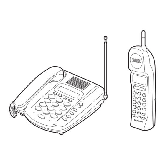
Base phone
SPECIFICATIONS
Base phone
Power source
DC 9V from AC power adaptor
Dimensions
Approx. 185 × 95 × 215 mm (w/h/d),
antenna excluded
(approx. 7
Antenna: Approx. 700 mm
(approx. 27
Mass
Approx. 755 g (approx. 27 oz)
Cordless handset charge cradle
Power source
DC 9V from AC power adaptor
Dimensions
Approx. 68 × 90 × 220 mm (w/h/d)
(approx. 2
Mass
Approx. 180 g (approx. 6 oz), wall bracket
included
Design and specifications are subject to
change without notice.
Cordless
handset
× 3
× 8
inches)
3/8
3/4
1/2
inches)
5/8
× 3
× 8
inches)
3/4
5/8
3/4
CORDLESS TELEPHONE
E Model
1
Advertisement
Table of Contents

Related Manuals for Sony SPP-888


Summary of Contents for Sony SPP-888
- Page 1 SPP-888 SERVICE MANUAL E Model Base phone Cordless handset SPECIFICATIONS Base phone General Dial signal Power source Tone, 10 PPS (pulse) selectable DC 9V from AC power adaptor Supplied accessories Dimensions Approx. 185 × 95 × 215 mm (w/h/d), See page 3.
-
Page 2: Table Of Contents
COMPONENTS IDENTIFIED BY MARK ! OR DOTTED LINE WITH MARK ! ON THE SCHEMATIC DIAGRAMS AND IN THE PARTS LIST ARE CRITICAL TO SAFE OPERATION. REPLACE THESE COMPONENTS WITH SONY PARTS WHOSE PART NUMBERS APPEAR AS SHOWN IN THIS MANUAL OR IN SUPPLEMENTS PUBLISHED BY SONY. -
Page 3: General
SECTION 1 GENERAL This section is extracted from instruction manual. -
Page 13: Disassembly
SECTION 2 DISASSEMBLY Note : Follow the disassembly procedure in the numerical order given. 2-1. CABINET (LOWER) 4 cabinet (lower) 2 P3x10 1 P3x10 2-2. BASE LCD BOARD 2 BTP2.6x8 1 CN301 3 BTP2.6x8 4 BASE LCD board... -
Page 14: Base Key Board
2-3. BASE KEY BOARD 1 CN302 2 BTP2.6x8 3 BTP2.6x8 4 BASE KEY board 2-4. BASE MIC BOARD 2 BTP2.6x8 3 BASE MIC board 1 Unsolder the 2 places. -
Page 15: Base Main Board
2-5. BASE MAIN BOARD 4 BTP2.6x8 5 BASE MAIN board 3 BTP2.6x8 2 BTP2.6x8 1 Unsolder the 2 places. 2-6. CABINET (REAR) 6 cabinet (rear) 1 battery case lid (hand) 2 BTP 2.6x10 5 claw 4 claws 3 claws... -
Page 16: Hand Main Board
2-7. HAND MAIN BOARD 5 Unsolder. discharge gap (CP101) 3 BTP 2x8 4 Unsolder the 3 places. 2 BTP 2x8 9 HAND MAIN board 0 BVTP 2x8 !™ HAND KEY board 1 CN3 8 Unsolder. 6 Unsolder. !¢ speaker !¡ charge terminals (hand) 7 Unsolder. -
Page 17: Test Mode
SECTION 3 TEST MODE BASE PHONE SECTION OPERATION AT START OF TEST MODE • The ringer sounds for 500 msec. • Setting of channel: CH1 for manual test mode and the Channel MANUAL TEST MODE Setting terminal for machine test mode. (See page 18.) Set the Test Mode: •... - Page 18 Channel Setting: During startup in machine test mode, make the following channel settings by loading the terminal input data. Pin No. TX frequency RX frequency TEST CLK COL3 COL2 COL1 COL0 (MHz) (MHz) Channel (TP320) (TP337) (TP336) (TP335) (TP334) 43.720 48.760 43.740 48.840...
-
Page 19: Handset Section
HANDSET SECTION OPERATION AT START OF TEST MODE • The ringer sounds for 500 msec. • Setting of channel: CH1 for manual test mode and the Channel MANUAL TEST MODE Setting terminal for machine test mode. (See page 20.) Set the Test Mode: •... - Page 20 Channel Setting: During startup in machine test mode, make the following channel settings by loading the terminal input data. Pin No. TX frequency RX frequency ROW5 COL4 COL3 COL2 COL1 (MHz) (MHz) Channel (TP205) (TP204) (TP203) (TP202) (TP201) 48.760 43.720 48.840 43.740 48.860...
- Page 21 2) EEPROM Read/Write test. Writes specific data into EEPROM and reads it displaying the following data on the LCD if it is normal and “EEPROM NG” if abnormal: “SONY CORPORATION” “1234567890” (character also displayed if any) 3) Manually stores the communication ID. After “ID=” is displayed, enter a four-digit communication ID in hexadecimal format.
-
Page 22: Electrical Adjustments
SECTION 4 ELECTRICAL ADJUSTMENTS BASE PHONE SECTION RX SECTION ADJUSTMENT RX DISCRI Adjustment Note: Note: • Apply 9V dc from regurated DC power supply. • Perform the adjustment at T3CH (28CH : 49.910 MHz) as a rule. • Perform the adjustment at T3CH (28CH : 49.910 MHz) as a rule. Setting : •... - Page 23 Adjustment Location : – base main board (component side) – S301 – base main board (conductor side) – TP10 50 Ω TP18 TP102 TP101...
-
Page 24: Handset Section
HANDSET SECTION RX SECTION ADJUSTMENT RX DISCRI Adjustment Note: Note: • Apply 3.6 V dc from regurated DC power supply. • Perform the adjustment at T1CH (26CH : 43.780 MHz) as a rule. • Perform the adjustment at T1CH (26CH : 43.780 MHz) as a rule. Setting : •... - Page 25 Adjustment Location : – hand main board (side A) – L101 – hand main board (side B) – TP23 TP22 TP103 TP28...
-
Page 26: Diagrams
SECTION 5 DIAGRAMS 5-1. IC PIN DESCRIPTION • IC401 LC662716A-4L38 (SYSTEM CONTROL) (HAND KEY BOARD) Pin No. Pin Name Pin Description BEEP-ATT Beep volume High/Low control output (L: High) TX-DATA RF transmission data output RINGER Beep output — Ground OSC1 —... -
Page 27: Block Diagram -Base Phone Section
SPP-888 5-2. BLOCK DIAGRAM — BASE PHONE SECTION — ANT1 TELESCOPIC ANTENNA RX DISCRI EXPANDER MIX, IF AMP, DET VOICE PROCESSOR D709 IC1 (2/3) IC1 (1/3) IC103 RECE MIC201 TX IN 10.68MHz 460kHz QUAD EXPANDER RAUX MICS MUTE TXAUX MIC+... -
Page 28: Block Diagram -Handset Section
SPP-888 5-3. BLOCK DIAGRAM — HANDSET SECTION — ANT2 TELESCOPIC ANTENNA EXPANDER RX DISCRI MIX, IF AMP, DET IC1 ( 2/3 ) IC1 ( 1/3 ) RECE MIX IN 10.68MHz BPF1 EXPANDER 460kHz MUTE SPEAKER D-COMP VOLUME RSSI CONTROL LOCAL... -
Page 29: Printed Wiring Board -Base Key Section
SPP-888 5-4. PRINTED WIRING BOARD — BASE KEY SECTION — 5-5. SCHEMATIC DIAGRAM — BASE KEY SECTION — (Page 33) (Page 30) Note on Schematic Diagram: • C : panel designation. • U : B+ Line. • Semiconductor Location Ref. No. -
Page 30: Printed Wiring Boards -Base Main Section
SPP-888 5-6. PRINTED WIRING BOARDS — BASE MAIN SECTION — • Semiconductor Location Ref. No. Location D-13 B-12 D104 H-13 D105 H-13 D106 H-13 D107 H-12 D108 G-13 D109 H-12 D111 G-11 D112 G-13 D113 D115 G-13 D116 G-13 D117... -
Page 31: Schematic Diagram -Base Main (1/3) Section
SPP-888 5-7. SCHEMATIC DIAGRAM — BASE MAIN (1/3) SECTION — (Page 32) (Page 33) Note: • All capacitors are in µF unless otherwise noted. pF: µµF • Power voltage is dc 9 V and fed with regulated dc power 50 WV or less are not indicated except for electrolytics supply from external power voltage jack. -
Page 32: Schematic Diagram -Base Main (2/3) Section
SPP-888 5-8. SCHEMATIC DIAGRAM — BASE MAIN (2/3) SECTION — • Refer to page 40 for IC Block Diagrams. (Page 31) Note: • All capacitors are in µF unless otherwise noted. pF: µµF • Power voltage is dc 12 V and fed with regulated dc power •... -
Page 33: Schematic Diagram -Base Main (3/3) Section
SPP-888 5-9. SCHEMATIC DIAGRAM — BASE MAIN (3/3) SECTION — • Refer to page 41 for IC Block Diagrams. (Page 31) (Page 29) (Page 35) Note: • All capacitors are in µF unless otherwise noted. pF: µµF • Power voltage is dc 9 V and fed with regulated dc power 50 WV or less are not indicated except for electrolytics supply from external power voltage jack. -
Page 34: Printed Wiring Board -Base Lcd Section
SPP-888 5-10. PRINTED WIRING BOARD — BASE LCD SECTION — • Semiconductor (Page 30) Location Ref. No. Location (D601) (D602) (D603) (D604) (D605) IC601 Q601 ) : SIDE A Note: • X : parts extracted from the component side. • b : Pattern from the side which enables seeing. -
Page 35: Schematic Diagram -Base Lcd Section
SPP-888 5-11. SCHEMATIC DIAGRAM — BASE LCD SECTION — • Refer to page 41 for IC Block Diagrams. (Page 33) Note: • All resistors are in Ω and W or less unless otherwise specified. • U : B+ Line. • Power voltage is dc 12 V and fed with regulated dc power supply from J101 with 100 Ω... -
Page 36: Printed Wiring Board -Hand Main Section
SPP-888 5-12. PRINTED WIRING BOARD — HAND MAIN SECTION — • Semiconductor Location Ref. No. Location D101 Q101 Q102 Q103 (Page 38) (Page 38) Note: • X : parts extracted from the component side. • Y : parts extracted from the conductor side. -
Page 37: Schematic Diagram -Hand Main Section
SPP-888 5-13. SCHEMATIC DIAGRAM — HAND MAIN SECTION — • Refer to page 40 for IC Block Diagrams. (Page 39) Note: • All capacitors are in µF unless otherwise noted. pF: µµF 50 WV or less are not indicated except for electrolytics and tantalums. -
Page 38: Printed Wiring Board -Hand Key Section
SPP-888 5-14. PRINTED WIRING BOARD — HAND KEY SECTION — (Page 36) (Page 36) • Semiconductor Location Ref. No. Location D201 D202 (D301) (D302) (D303) (D304) (D305) (D306) (D307) (D308) D401 D402 D403 D404 D405 D406 IC201 IC202 IC301 IC401... -
Page 39: Schematic Diagram -Hand Key Section
SPP-888 5-15. SCHEMATIC DIAGRAM — HAND KEY SECTION — • Refer to page 41 for IC Block Diagrams. (Page 37) Note: • All capacitors are in µF unless otherwise noted. pF: µµF • Voltage is dc with respect to ground under no-signal 50 WV or less are not indicated except for electrolytics condition. - Page 40 • IC Block Diagrams IC1 TB31224F (HAND MAIN board) IC103 TEA1099H/C1.551 (BASE MAIN board) NOISE E-RECT N-REC VCC1 FILTER GND1 41 40 39 38 37 VREF IF AMP QUOD DATA LACHA MIXER MIXER COMPARATOR DETECT RSSI BATTERY VCC2 ALARM RECEIVE SUPPLY POWER-DOWN ANALOG...
- Page 41 IC201 S-80730AL-AT-T1 (BASE MAIN board) IC301 S-24C01AFJA-TB-01 (BASE MAIN board) IC404 S-80727AL-AQ-T1 (HAND KEY board) VOLTAGE ADDRESS COUNTER SENSE AMP MEMORY CONTROL CONTROL LOGIC Y DECODER CONTROL PAGE BUFFER LOGIC EEPROM ARRAY HV PUMP IC601 LC75834JED (BASE LCD board) 33 32 31 30 29 28 27 26 25 24 23 COM4 COMMON...
- Page 42 IC302 LC662516A-4L37 (BASE MAIN board) P20/SI0 P21/SO0 P22/SCK0 P23/INT0 P30/INT1 P31/POUT0 P32/POUT1 PD3/INV4O PD2/INV4I PRESCALER STACK INTERRUPT PD1/INV30 (512W) CONTROL OSC1 PD0/INV3I OSC2 PC3/INV2O PC2/INV2I SYSTEM CONTROL TEST P33/HOLD P40/INV0I P41/INV0O P42/INV1I P43/INV1O TIMER TIMER P53/INT2 P60/SI1/ML P61/SO1/DP P62/SCK1/DT P63/PIN1 SERIAL SERIAL I/O 1...
- Page 43 IC301 RH5RL30AA-T1 (HAND KEY board) IC402 24LC16BT/SN (HAND KEY board) SENSE AMP MEMORY CONTROL CONTROL LOGIC Y DECODER CONTROL LOGIC PAGE LATCH EEPROM ARRAY X DECODER (256 x 8) HV GENERATOR...
-
Page 44: Exploded Views
SECTION 6 EXPLODED VIEWS NOTE: • The mechanical parts with no reference • -XX and -X mean standardized parts, so • Accessories and packing materials are number in the exploded views are not supplied. they may have some difference from the given in the last of this parts list. -
Page 45: Handset Section
6-2. HANDSET SECTION CP101 ANT2 MIC401 LCD1 Ref. No. Part No. Description Remark Ref. No. Part No. Description Remark 3-025-399-01 WINDOW (LCD) 3-025-398-01 LID (HAND), BATTERY CASE 3-027-148-01 SHEET (WINDOW), ADHESIVE 3-371-765-21 SCREW (2X8), +BTP 3-025-401-01 TERMINAL (HAND), CHARGE 7-685-134-19 SCREW +BTP 2.6X8 TYPE2 N-S 1-771-405-61 SWITCH, RUBBER KEY 7-685-535-14 SCREW +BTP 2.6X10 TYPE2 N-S 3-025-829-01 HOLDER, ANTENNA... -
Page 46: Electrical Parts List
BASE KEY BASE LCD SECTION 7 ELECTRICAL PARTS LIST BASE MAIN NOTE: • Due to standardization, replacements in • Items marked “*” are not stocked since The components identified by mark ! or dotted line with mark. the parts list may be different from the they are seldom required for routine service. - Page 47 BASE MAIN Ref. No. Part No. Description Remark Ref. No. Part No. Description Remark 1-115-566-11 CERAMIC CHIP 4.7uF C128 1-126-963-11 ELECT 4.7uF 1-163-241-11 CERAMIC CHIP 39PF C129 1-163-021-11 CERAMIC CHIP 0.01uF 1-163-038-00 CERAMIC CHIP 0.1uF C130 1-164-004-11 CERAMIC CHIP 0.1uF 1-163-021-11 CERAMIC CHIP 0.01uF C131...
- Page 48 BASE MAIN Ref. No. Part No. Description Remark Ref. No. Part No. Description Remark < CONNECTOR > J201 1-779-207-11 JACK, DC (POLARITY UNIFIED TYPE) (DC IN 9V) * CN301 1-785-661-11 PIN, CONNECTOR (PC BOARD) 9P * CN302 1-785-665-11 PIN, CONNECTOR (PC BOARD) 13P <...
- Page 49 BASE MAIN Ref. No. Part No. Description Remark Ref. No. Part No. Description Remark JC51 1-216-296-00 SHORT 1-216-037-00 METAL CHIP 1/10W JC52 1-216-296-00 SHORT 1-216-097-00 RES,CHIP 100K 1/10W JC53 1-216-296-00 SHORT 1-216-085-00 METAL CHIP 1/10W JC61 1-216-295-00 SHORT 1-216-019-00 METAL CHIP 1/10W JC62 1-216-295-00 SHORT...
- Page 50 BASE MAIN Ref. No. Part No. Description Remark Ref. No. Part No. Description Remark R125 1-216-044-00 METAL CHIP 1/10W R205 1-216-033-00 METAL CHIP 1/10W R126 1-216-062-00 METAL CHIP 3.6K 1/10W R206 1-216-061-00 METAL CHIP 3.3K 1/10W R127 1-216-057-00 METAL CHIP 2.2K 1/10W R207...
- Page 51 BASE MAIN BASE MIC HAND KEY Ref. No. Part No. Description Remark Ref. No. Part No. Description Remark < VARIABLE RESISTOR > C404 1-164-505-11 CERAMIC CHIP 2.2uF C405 1-163-021-11 CERAMIC CHIP 0.01uF 1-241-770-11 RES, ADJ, CARBON 1M C406 1-135-181-21 TANTALUM CHIP 4.7uF 6.3V RV201 1-249-439-11 CARBON...
- Page 52 HAND KEY Ref. No. Part No. Description Remark Ref. No. Part No. Description Remark < MICROPHONE > R318 1-216-033-00 METAL CHIP 1/10W R319 1-216-025-00 RES,CHIP 1/10W MIC401 1-542-349-11 MICROPHONE, ELECTRET CONDENSER R320 1-216-025-00 RES,CHIP 1/10W R321 1-216-025-00 RES,CHIP 1/10W < TRANSISTOR > R322 1-216-025-00 RES,CHIP 1/10W...
- Page 53 HAND MAIN Ref. No. Part No. Description Remark Ref. No. Part No. Description Remark A-3672-744-A HAND MAIN BOARD, COMPLETE C111 1-163-227-11 CERAMIC CHIP 10PF 0.5PF C112 1-163-239-11 CERAMIC CHIP 33PF *************************** C113 1-163-243-11 CERAMIC CHIP 47PF < BPF > C114 1-162-587-11 CERAMIC CHIP 0.039uF C115...
- Page 54 SPP-888 HAND MAIN Ref. No. Part No. Description Remark Ref. No. Part No. Description Remark 1-216-037-00 METAL CHIP 1/10W MISCELLANEOUS 1-216-073-00 METAL CHIP 1/10W *************** 1-216-049-11 RES,CHIP 1/10W 1-216-097-00 RES,CHIP 100K 1/10W 1-775-798-41 CORD, CURL (BASE PHONE) 1-216-021-00 METAL CHIP...
Need help?
Do you have a question about the SPP-888 and is the answer not in the manual?
Questions and answers