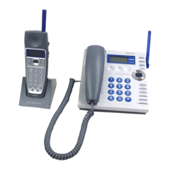
Sony SPP-S2730 Service Manual
Hide thumbs
Also See for SPP-S2730:
- Operating instructions manual (84 pages) ,
- Specifications (2 pages)
Table of Contents
Advertisement
Quick Links
SERVICE MANUAL
Ver 1.2 2002.01
General
Spread method
Direct-Sequence Spread-Spectrum
Access method
FDMA-TDD
Frequency band
2.4075 - 2.4720 GHz
Operating channel
40 channels
Dial signal
Tone, 10 PPS (pulse) selectable
Supplied accessories
AC power adaptor for the base phone
(AC-T46)
Charger/AC power adaptor for the charger
(AC-T127)
Handset
Handset cord
Telephone line cords (2)
Wall bracket/stand for base phone
Rechargeable battery pack (BP-T38)
Sony Corporation
9-873-167-03
2002A0500-1
Personal Audio Company
C 2002.1
Published by Sony Engineering Corporation
SPP-S2730
SPECIFICATIONS
Cordless handset
Power source
Rechargeable battery pack BP-T38
Battery life
Standby: Approx. 6 days
Talk:
Approx. 5 hours
Battery charging time
Approx. 12 hours
Dimensions
3
5
15
Approx. 2
⁄
x 6
⁄
x 1
⁄
inches (w/h/d),
8
8
16
antenna excluded
(approx. 58 x 166 x 48 mm)
7
Antenna: Approx. 2
⁄
inches
8
(approx. 72 mm)
Mass
Approx. 8.1 oz
(approx. 230 g), battery included
Base phone
Power source
DC 9V from AC power adaptor
AC-T46
US Model
Canadian Model
Dimensions
3
3
1
Approx. 7
⁄
x 3
⁄
x 8
⁄
8
4
8
antenna excluded
(approx. 187 x 93 x 206 mm)
3
Antenna: Approx. 4
⁄
inches
8
(approx. 108 mm)
Mass
Approx. 1 lb 8 oz
(approx. 680 g), wall bracket excluded
Charger
Power source
DC 9V from AC power adaptor
AC-T127
Dimensions
1
5
1
Approx. 3
⁄
x 2
⁄
x 4
⁄
4
8
8
(approx. 80 x 64 x 102 mm)
Mass
Approx. 2.7 oz (approx. 75 g)
Design and specifications are subject to
change without notice.
CORDLESS TELEPHONE
inches (w/h/d),
inches (w/h/d)
Advertisement
Table of Contents

Related Manuals for Sony SPP-S2730


Summary of Contents for Sony SPP-S2730
- Page 1 Wall bracket/stand for base phone Power source Rechargeable battery pack (BP-T38) DC 9V from AC power adaptor Design and specifications are subject to AC-T46 change without notice. CORDLESS TELEPHONE Sony Corporation 9-873-167-03 2002A0500-1 Personal Audio Company C 2002.1 Published by Sony Engineering Corporation...
-
Page 2: Table Of Contents
SONY PARTS WHOSE PART NUMBERS APPEAR AS DE FONCTIONNEMENT. NE REMPLACER CES COM- SHOWN IN THIS MANUAL OR IN SUPPLEMENTS PUB- POSANTS QUE PAR DES PIÈCES SONY DONT LES LISHED BY SONY. NUMÉROS SONT DONNÉS DANS CE MANUEL OU DANS LES SUPPLÉMENTS PUBLIÉS PAR SONY. -
Page 3: Servicing Notes
SPP-S2730 SECTION 1 SERVICING NOTES IF AN ERROR MESSAGE IS DISPLAYED If the following error message is displayed after the power was turned on, check the items where “1” is indicated. [][] [][] ERROR= t Write correct data to the EEPROM. -
Page 4: General
SPP-S2730 SECTION 2 This section is extracted from instruction manual. GENERAL Identifying the parts Refer to the pages indicated in parentheses for details. Base phone 1 Display window (p. 35, 60) qa VOL – button (p. 35) Adjusts the handset or speaker 2 VOICE MAIL lamp (p. - Page 5 SPP-S2730 qj INTERCOM button (p. 55) wa Antenna (p. 12, 71) Lets you talk between the base ws Hook for AC power adaptor phone and cordless handset. cord (p. 12, 71) qk HOLD button (p. 36) wd DC IN 9V jack (p. 12, 71) Puts a call on hold.
- Page 6 SPP-S2730 Identifying the parts (continued) Cordless handset 1 Antenna 8 EZ ACCESS button (p. 23, 33) Lets you make a call with the 2 Speaker registered access number. 3 Display window (p. 32, 60) 9 Jog Dial (p. 17, 43, 61) 4 TALK button (p.
- Page 7 SPP-S2730 TONE button (p. 33) ql PGM (program) button (p. 17, 43) Allows you to switch temporarily to tone dialing. w; REDIAL/PAUSE button (p. 24, 37) qg RINGER Redials one of the last five numbers qh I (HEADSET) jack (p. 33, 39, 72) called/inserts a pause in the dialing sequence.
-
Page 8: Registering Additional Cordless Handsets
SPP-S2730 Registering additional cordless handsets The phone system includes a cordless handset. You can expand the system including a total of four cordless handsets. Be sure to register the ID number of the additional cordless handset called “station number” to the base phone before using the additional cordless handset. - Page 9 SPP-S2730 Registering additional cordless handsets (continued) Enter the 10 digits system ID by pressing the dialing keys. The system ID is shown on a sticker affixed to the bottom of the base phone. Press (PGM). You hear a long confirmation beep and the assigned station number is displayed.
-
Page 10: Disassembly
SPP-S2730 SECTION 3 DISASSEMBLY • This set can be disassembled in the order shown below. 3-1. DISASSEMBLY FLOW Cabinet (rear) Hand Main Board Base Cabinet (lower) Assy Base Key Board Base Main Board Note: Follow the disassembly procedure in the numerical order given. -
Page 11: Base Cabinet (Lower) Assy
SPP-S2730 3-4. BASE CABINET (LOWER) ASSY 1 four screws (P3 × 10) 5 base cabinet (lower) assy 4 two connectors (CN301, CN302) 3 connector (CN172) 3-5. BASE KEY BOARD 1 ten screws (BTP2.6 × 8) 2 BASE KEY board... -
Page 12: Base Main Board
SPP-S2730 3-6. BASE MAIN BOARD 2 four screws (BTP2.6 × 8) 3 BASE MAIN board 1 Remove two solders. -
Page 13: Test Mode
SPP-S2730 SECTION 4 TEST MODE 2. In this test mode, rotate the jog dial up/down or press the jog BASE UNIT dial, or turn on/off the hook switch to respective status will be displayed on the LCD as follows. [ENTERING THE TEST MODE] Up the jog dial : “UP”... - Page 14 SPP-S2730 4. TEST MODE E (EEPROM Read/Write Mode) Contents of EEPROM data: In the test mode idling status, press the key to active this mode Address Data (hexadecimal) and display as below. (hexadecimal) 1st byte 2nd byte 3rd byte 4th byte...
-
Page 15: Handset
SPP-S2730 6. TEST MODE B (Writing the ID number) HANDSET Note: Though the “TEST MODE E” handles the ID numbers as hexa- decimal numbers, the “TEST MODE B” handles them as decimal [ENTERING THE TEST MODE] numbers. Both are different in numerical notation format only, and 1. - Page 16 SPP-S2730 1-2. Jog Test 3. TEST MODE D (RF Control Mode) 1. In the “TEST A” status, press the key to active the jog test In the test mode idling status, press the key to active this mode and display as below.
- Page 17 H-No. : Number of registered handset M-No. : Number of model destination (SPP-S2730: 80h) 5. TEST MODE B (Writing the ID number) Note: Though the “TEST MODE E” handles the ID numbers as hexa- decimal numbers, the “TEST MODE B” handles them as decimal numbers.
-
Page 18: Rf Testing
SPP-S2730 Ver 1.1 Test mode setting: RF TESTING – Base Unit – [ERASE] 1. Press three keys of , and simultaneously to This test is for checking the RF system without disassembling the enter the test mode. set in servicing. Perform measurement using the spectrum ana- 2. - Page 19 SPP-S2730 Ver 1.1 REF –10.0 dBm MKR 2.44076 GHz 1-3. TX Power Check 10dB/ A_View Posi B_Blank Norm –14.52 dBm Spectrum analyzer setting: MARKER 2 . 4 4 0 7 6 GHz Center frequency: 2440.5 MHz Span : 10 MHz...
-
Page 20: Electrical Adjustments
SPP-S2730 SECTION 5 ELECTRICAL ADJUSTMENTS Between Microphone and Line Signal Level 0 dBm = 0.775 V Measurement Setting: BASE UNIT feeding bridge Base unit • Make the set in the test mode. (See page 13) Line TP101 Line TP102 Power Failure Test... - Page 21 SPP-S2730 Between Microphone in the Local Handset and TX Current Measurement Speaker in the Local Handset (CODEC Loop Back) Setting: Signal Level Measurement Base unit regulated dc Note: No test mode in this measurement. power supply Setting: TP201 audio analyzer +9 V 1.2 kHz, –27 dBm...
-
Page 22: Handset
SPP-S2730 Current Measurement HANDSET Setting: • Make the set in the test mode. (See page 15) Handset regulated dc power supply Power Failure Test Procedure: TP101 1. In the test mode idling status, press the key to display +3.8 V “TEST A”. - Page 23 SPP-S2730 Between Microphone and Speaker (CODEC Loop Frequency Deviation Measurement Back) Signal Level Measurement (H to H Gain Up) Setting: Setting: Same as step 5. antenna pick-up coil Procedure: 1. In the step 5 “Between Microphone and Speaker (CODEC Loop Back) Signal Level Measurement” status, press the key of the handset.
- Page 24 SPP-S2730 Connecting Location: – BASE MAIN BOARD (Conductor Side) – – BASE MAIN BOARD (Component Side) – TP202 TP201 TP102 TP101 RF271 (RF UNIT) 12 13 TP472 (LHS SP GND) R288 R287 TP307 TP474 R285 (LHS MIC GND) TP306 (GND)
-
Page 25: Diagrams
SPP-S2730 SECTION 6 DIAGRAMS 6-1. BLOCK DIAGRAM – BASE UNIT Section – ANT101 (MAIN ANTENNA) ANT102 TEL LINE IC402 (SUB ANTENNA) • SIGNAL PATH B+ SWITCH F101 RF271 Q105 RF UNIT : RX D107 – 110 T101 MJ101 (DL0) L OUT... -
Page 26: Block Diagram - Handset Section
SPP-S2730 6-2. BLOCK DIAGRAM – HANDSET Section – CODEC ANT201 RF61 (ANTENNA) RF UNIT MUTING PCMRO PCMRI VFRO ATTENUATOR AF AMP RXAD PCM L. P. F. EXPANDER CONVERTER 8 ANT ADPCM (SPEAKER) PCMSI PCMSO AIN– MIC AMP MIC1 TXAD PCM B. -
Page 27: Note For Printed Wiring Boards And Schematic Diagrams
SPP-S2730 6-3. NOTE FOR PRINTED WIRING BOARDS AND SCHEMATIC DIAGRAMS • Waveforms – HAND MAIN Board – – BASE MAIN Board – Note on Printed Wiring Board: Note on Schematic Diagram: 1 IC301 tk (CF2) 3 IC1 wl (BCLK) • All capacitors are in µF unless otherwise noted. pF: µµF •... -
Page 28: Printed Wiring Board
SPP-S2730 6-4. PRINTED WIRING BOARD – BASE MAIN Board (Component Side) – • See page 27 for Note on Printed Wiring Board. • Semiconductor Location BASE MAIN BOARD (COMPONENT SIDE) Ref. No. Location IC102 IC203 IC301 ANT101 MAIN IC302 ANTENNA... -
Page 29: Printed Wiring Boards - Base Main (Conductor Side)/Base Mic Boards
SPP-S2730 Ver 1.1 6-5. PRINTED WIRING BOARDS – BASE MAIN (Conductor Side)/BASE MIC Boards – • See page 27 for Note on Printed Wiring Board. • Semiconductor J201 5 3 1 2 4 6 Location MJ101 – LINE DC IN 9V Ref. -
Page 30: Schematic Diagram – Base Main Board (1/3)
SPP-S2730 6-6. SCHEMATIC DIAGRAM – BASE MAIN Board (1/3) – • See page 27 for Waveform. • See page 27 for Note on Schematic Diagram. TP203 R333 R335 R334 4.7k 4.7M R346 R336 C318 C315 X301 R347 6MHz 100k CN301... -
Page 31: Schematic Diagram - Base Main (2/3)/Base Mic Boards
SPP-S2730 6-7. SCHEMATIC DIAGRAM – BASE MAIN (2/3)/BASE MIC Boards – • See page 27 for Note on Schematic Diagram. (Page 30) L455 L477 L479 TP475 MIC401 R492 R493 L480 2.2k L456 L478 C497 C500 L475 CN172 TP476 SP401 L476... -
Page 32: Schematic Diagram - Base Main Board (1/3)
SPP-S2730 6-8. SCHEMATIC DIAGRAM – BASE MAIN Board (3/3) – • • See page 27 for Waveform. • See page 33 for IC Block Diagram. See page 27 for Note on Schematic Diagram. (Page 30) TP425 C403 C402 R411 R410... - Page 33 SPP-S2730 • IC Block Diagrams – BASE MAIN Board – – HAND MAIN Board – IC401 NJM2072M (TE2) ML7079MBZ020 BCLK INPUT SYNC OUTPUT2 AIN – 3 – PCMSO B. P. F. CONVERTER COMPRESSOR GAIN CONT NC 4 20kΩ OUTPUT1 VREF...
-
Page 34: Printed Wiring Boards - Base Key/Key Jog Boards
SPP-S2730 6-9. PRINTED WIRING BOARDS – BASE KEY/KEY JOG Boards – • See page 27 for Note on Printed Wiring Board. • Semiconductor LCD101 Location LIQUID CRYSTAL DISPLAY PANEL Ref. No. Location BASE KEY BOARD D705 D706 D707 D708 D709... -
Page 35: Schematic Diagram - Base Key/Key Jog Boards
SPP-S2730 6-10. SCHEMATIC DIAGRAM – BASE KEY/KEY JOG Boards – • See page 27 for Note on Schematic Diagram. CN701 TP751 TP752 TP753 TP754 TP755 C703 TP756 C704 TP757 R702 560k C705 TP758 LCD101 C706 TP759 LIQUID R703 C707 TP760... -
Page 36: Printed Wiring Board - Hand Main Board
SPP-S2730 6-11. PRINTED WIRING BOARD – HAND MAIN Board – • See page 27 for Note on Printed Wiring Board. HAND MAIN BOARD (COMPONENT SIDE) BZ101 6 54 CHARGE TERMINAL 1 23 TP5 (MIC GND) ANT201 MIC1 1-682-517- (11) D122 – 128 (SPEAKER) D125 –... -
Page 37: Schematic Diagram - Hand Main Board (1/2)
SPP-S2730 6-12. SCHEMATIC DIAGRAM – HAND MAIN Board (1/2) – • • See page 27 for Waveforms. • See page 33 for IC Block Diagram. See page 27 for Note on Schematic Diagram. RF61 (RF UNIT) 1000 6.3V TP62 ANT201... -
Page 38: Schematic Diagram - Hand Main Board (2/2)
SPP-S2730 6-13. SCHEMATIC DIAGRAM – HAND MAIN Board (2/2) – • • See page 33 for IC Block Diagram. See page 27 for Note on Schematic Diagram. CN121 8.2 H 8.2 H 8.2 H C131 C132 R139 C133 LCD201 C134... -
Page 39: Ic Pin Function Description
SPP-S2730 6-14. IC PIN FUNCTION DESCRIPTION • BASE MAIN BOARD IC301 SB875064W-5W61 (SYSTEM CONTROLLER) Description Pin No. Pin Name SS SPI CLK Serial data transfer clock signal output to the RF unit (RF271) LCD SDA Two-way data bus with the liquid crystal display module (LCD101) LCD CS Chip select signal output to the liquid crystal display module (LCD101) “L”... - Page 40 SPP-S2730 Description Pin No. Pin Name Power fail detection signal input “L”: power fail AC POWER FAIL SS IRQ Interrupt request signal input from the RF unit (RF271) “L” active System reset signal input from the reset signal generator (IC302) “L”: reset RESET For several hundreds msec.
- Page 41 SPP-S2730 • BASE MAIN BOARD IC402 DL16121B11AQC (DSP) Description Pin No. Pin Name AGPIO5 to 1 to 9 Not used (open) AGPIO13 AGPIO14 MIC gain control signal output “L”: MIC REC AGPIO15 Not used (open) — Power supply terminal (+5V) —...
- Page 42 SPP-S2730 Pin No. Pin Name Description Power down control signal input from the system controller (IC301) “L”: power down Chip enable signal output to the flash memory “L” active FCSN0 Not used (open) GPIO1 Not used (open) HCSN1 Chip select signal input from the system controller (IC301) “L” active...
- Page 43 SPP-S2730 • HAND MAIN BOARD IC121 SH875048W-5W62 (SYSTEM CONTROLLER) Pin No. Pin Name Description SS SPI CLK Serial data transfer clock signal output to the RF unit (RF61) LCD SDA Two-way data bus with the liquid crystal display module (LCD201) LCD CS Chip select signal output to the liquid crystal display module (LCD201) “L”...
- Page 44 SPP-S2730 Description Pin No. Pin Name DIS CHG Wakeup control signal output “L” output when discharge (WAKE UP) Watch dog timer reset signal input terminal “H”: reset Not used (fixed at “L”) WAKE UP Wakeup control signal input “H”: wakeup...
-
Page 45: Exploded Views
SPP-S2730 SECTION 7 EXPLODED VIEWS NOTE: • -XX and -X mean standardized parts, so they • Items marked “*” are not stocked since they The components identified by mark 0 or dotted line with mark 0 are may have some difference from the original are seldom required for routine service. -
Page 46: Base Set
SPP-S2730 Ver 1.2 7-2. BASE SET not supplied SP401 ANT102 LCD101 ANT101 Ref. No. Part No. Description Remark Ref. No. Part No. Description Remark 3-936-696-21 FOOT, RUBBER 3-230-657-01 DIAL (JOG) X-3380-786-1 CABINET (LOWER) ASSY 3-230-659-01 BUTTON (VOL) 3-230-652-01 STOPPER (ANTENNA) -
Page 47: Electrical Parts List
SPP-S2730 SECTION 8 ELECTRICAL PARTS LIST BASE KEY BASE MAIN NOTE: • Due to standardization, replacements in the • Items marked “*” are not stocked since they The components identified by 0 or dotted line with mark mark parts list may be different from the parts speci- are seldom required for routine service. - Page 48 SPP-S2730 BASE MAIN Ref. No. Part No. Description Remark Ref. No. Part No. Description Remark C145 1-216-864-11 METAL CHIP 1/16W C459 1-162-964-11 CERAMIC CHIP 0.001uF C146 1-117-863-11 CERAMIC CHIP 0.47uF 6.3V C460 1-162-962-11 CERAMIC CHIP 470PF C147 1-126-935-11 ELECT 470uF...
- Page 49 SPP-S2730 BASE MAIN Ref. No. Part No. Description Remark Ref. No. Part No. Description Remark IC303 6-700-340-01 IC CAT24WC32JI-1.8-TE13 Q107 8-729-905-34 TRANSISTOR 2SC4081T106Q IC401 8-759-701-51 IC NJM2072M (TE2) Q303 8-729-905-34 TRANSISTOR 2SC4081T106Q IC402 6-700-475-01 IC DL16121B11AQC Q401 8-729-905-34 TRANSISTOR 2SC4081T106Q...
- Page 50 SPP-S2730 BASE MAIN Ref. No. Part No. Description Remark Ref. No. Part No. Description Remark R278 1-216-864-11 METAL CHIP 1/16W R347 1-216-845-11 METAL CHIP 100K 1/16W R279 1-216-864-11 METAL CHIP 1/16W R358 1-216-864-11 METAL CHIP 1/16W R359 1-216-864-11 METAL CHIP...
- Page 51 SPP-S2730 BASE MAIN BASE MIC HAND MAIN Ref. No. Part No. Description Remark Ref. No. Part No. Description Remark R453 1-216-829-11 METAL CHIP 4.7K 1/16W < LINE TRANSFORMER > R463 1-216-833-11 METAL CHIP 1/16W 0 T101 1-435-721-11 LINE TRANSFORMER R464...
- Page 52 SPP-S2730 HAND MAIN Ref. No. Part No. Description Remark Ref. No. Part No. Description Remark 1-164-505-11 CERAMIC CHIP 2.2uF D121 8-719-988-61 DIODE 1SS355TE-17 1-162-908-11 CERAMIC CHIP 0.25PF 50V D122 8-719-081-03 LED PY1111C-730-TR (LCD BACK LIGHT) 1-162-908-11 CERAMIC CHIP 0.25PF 50V...
- Page 53 SPP-S2730 HAND MAIN Ref. No. Part No. Description Remark Ref. No. Part No. Description Remark (TYPE B) 1-216-864-11 METAL CHIP 1/16W 1-216-823-11 METAL CHIP 1.5K 1/16W 1-216-864-11 METAL CHIP 1/16W (TYPE A) 1-216-864-11 METAL CHIP 1/16W < MICROPHONE > 1-216-845-11 METAL CHIP...
- Page 54 SPP-S2730 HAND MAIN KEY JOG Ref. No. Part No. Description Remark Ref. No. Part No. Description Remark R147 1-216-809-11 METAL CHIP 1/16W R148 1-216-809-11 METAL CHIP 1/16W ************** R149 1-216-821-11 METAL CHIP 1/16W HARDWARE LIST R150 1-216-845-11 METAL CHIP 100K...
- Page 55 SPP-S2730 MEMO...
-
Page 56: Revision History
SPP-S2730 REVISION HISTORY Clicking the version allows you to jump to the revised page. Also, clicking the version at the upper right on the revised page allows you to jump to the next revised page. Ver. Date Description of Revision 2001.06...
Need help?
Do you have a question about the SPP-S2730 and is the answer not in the manual?
Questions and answers